2SK3530. Аналоги и основные параметры
Наименование производителя: 2SK3530
Тип транзистора: MOSFET
Полярность: N
Предельные значения
Pd ⓘ
- Максимальная рассеиваемая мощность: 70 W
|Vds|ⓘ - Максимально допустимое напряжение сток-исток: 800 V
|Vgs|ⓘ - Максимально допустимое напряжение затвор-исток: 30 V
|Id| ⓘ - Максимально допустимый постоянный ток стока: 7 A
Tj ⓘ - Максимальная температура канала: 150 °C
Электрические характеристики
tr ⓘ -
Время нарастания: 8 ns
Cossⓘ - Выходная емкость: 105 pf
RDSonⓘ - Сопротивление сток-исток открытого транзистора: 1.9 Ohm
Тип корпуса: TO-220F
Аналог (замена) для 2SK3530
- подборⓘ MOSFET транзистора по параметрам
2SK3530 даташит
..1. Size:114K fuji
2sk3530.pdf 

2SK3530-01MR 200304 FUJI POWER MOSFET N-CHANNEL SILICON POWER MOSFET Super FAP-G Series Outline Drawings [mm] TO-220F Features High speed switching Low on-resistance No secondary breadown Low driving power Avalanche-proof Applications Switching regulators UPS (Uninterruptible Power Supply) DC-DC converters Maximum ratings and characteristicAbsolute maximum ratings (Tc=25 C unl
..2. Size:189K inchange semiconductor
2sk3530.pdf 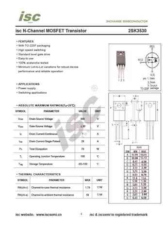
isc N-Channel MOSFET Transistor 2SK3530 FEATURES With TO-220F packaging High speed switching Standard level gate drive Easy to use 100% avalanche tested Minimum Lot-to-Lot variations for robust device performance and reliable operation APPLICATIONS Power supply Switching applications ABSOLUTE MAXIMUM RATINGS(T =25 ) a SYMBOL PARAMETER VALUE UNIT V Drain-So
8.1. Size:221K toshiba
2sk3538.pdf 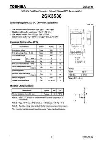
2SK3538 TOSHIBA Field Effect Transistor Silicon N Channel MOS Type ( -MOSV) 2SK3538 Switching Regulator, DC-DC Converter Applications Unit mm Low drain-source ON resistance R = 75 m (typ.) DS (ON) High forward transfer admittance Yfs = 7.0 S (typ.) Low leakage current I = 100 A (V = 500 V) DSS DS Enhancement-mode V = 2.0 to 4.0 V (V = 10 V, I = 1 m
8.2. Size:107K panasonic
2sk3539.pdf 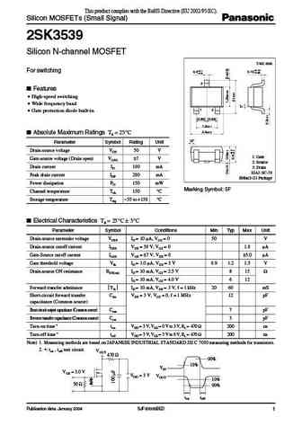
This product complies with the RoHS Directive (EU 2002/95/EC). Silicon MOSFETs (Small Signal) 2SK3539 Silicon N-channel MOSFET Unit mm For switching 0.15+0.10 0.3+0.1 0.05 0.0 3 Features High-speed switching Wide frequency band 1 2 Gate protection diode built-in (0.65) (0.65) 1.3 0.1 2.0 0.2 Absolute Maximum Ratings Ta = 25 C 10 Parameter Sym
8.3. Size:252K panasonic
2sk3539g0l.pdf 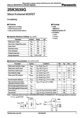
This product complies with the RoHS Directive (EU 2002/95/EC). Silicon MOSFETs (Small Signal) 2SK3539G Silicon N-channel MOSFET For switching Package Features Code High-speed switching SMini3-F2 Wide frequency band Marking Symbol 5F Gate protection diode built-in Pin Name 1 Gate 2 Source Absolute Maximum Ratings Ta = 25 C 3 Drain Parame
8.4. Size:116K fuji
2sk3533-01.pdf 
2SK3533-01 200304 FUJI POWER MOSFET N-CHANNEL SILICON POWER MOSFET Super FAP-G Series Outline Drawings [mm] TO-220AB Features High speed switching Low on-resistance No secondary breadown Low driving power Avalanche-proof Applications Switching regulators UPS (Uninterruptible Power Supply) DC-DC converters Maximum ratings and characteristicAbsolute maximum ratings (Tc=25 C unle
8.5. Size:110K fuji
2sk3531-01.pdf 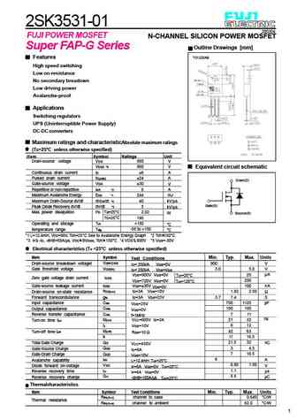
2SK3531-01 200304 FUJI POWER MOSFET N-CHANNEL SILICON POWER MOSFET Super FAP-G Series Outline Drawings [mm] TO-220AB Features High speed switching Low on-resistance No secondary breadown Low driving power Avalanche-proof Applications Switching regulators UPS (Uninterruptible Power Supply) DC-DC converters Maximum ratings and characteristicAbsolute maximum ratings (Tc=25 C unle
8.6. Size:112K fuji
2sk3535-01.pdf 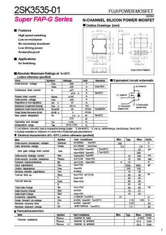
FUJI POWER MOSFET 2SK3535-01 200304 Super FAP-G Series N-CHANNEL SILICON POWER MOSFET Outline Drawings [mm] Features High speed switching Low on-resistance No secondary breadown Low driving power Avalanche-proof Applications for Switching Foot Print Pattern Absolute Maximum Ratings at Tc=25 C ( unless otherwise specified) Item Symbol Ratings Unit Remarks Equivalent circuit sche
8.7. Size:110K fuji
2sk3532-01mr.pdf 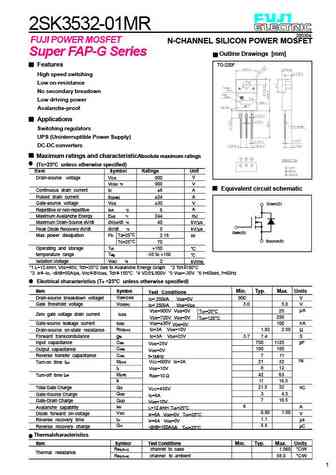
2SK3532-01MR 200304 FUJI POWER MOSFET N-CHANNEL SILICON POWER MOSFET Super FAP-G Series Outline Drawings [mm] Features TO-220F High speed switching Low on-resistance No secondary breadown Low driving power Avalanche-proof Applications Switching regulators UPS (Uninterruptible Power Supply) DC-DC converters Maximum ratings and characteristicAbsolute maximum ratings (Tc=25 C unle
8.8. Size:117K fuji
2sk3534-01mr.pdf 
2SK3534-01MR 200304 FUJI POWER MOSFET N-CHANNEL SILICON POWER MOSFET Super FAP-G Series Outline Drawings [mm] Features TO-220F High speed switching Low on-resistance No secondary breadown Low driving power Avalanche-proof Applications Switching regulators UPS (Uninterruptible Power Supply) DC-DC converters Maximum ratings and characteristicAbsolute maximum ratings (Tc=25 C unle
8.9. Size:112K fuji
2sk3537-01mr.pdf 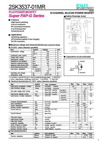
2SK3537-01MR 200304 FUJI POWER MOSFET N-CHANNEL SILICON POWER MOSFET Outline Drawings [mm] Super FAP-G Series TO-220F Features High speed switching Low on-resistance No secondary breadown Low driving power Avalanche-proof Applications Switching regulators UPS (Uninterruptible Power Supply) DC-DC converters Maximum ratings and characteristicAbsolute maximum ratings (Tc=25 C un
8.10. Size:114K fuji
2sk3532.pdf 
2SK3532-01MR 200304 FUJI POWER MOSFET N-CHANNEL SILICON POWER MOSFET Super FAP-G Series Outline Drawings [mm] Features TO-220F High speed switching Low on-resistance No secondary breadown Low driving power Avalanche-proof Applications Switching regulators UPS (Uninterruptible Power Supply) DC-DC converters Maximum ratings and characteristicAbsolute maximum ratings (Tc=25 C unle
8.11. Size:289K inchange semiconductor
2sk3533-01.pdf 
isc N-Channel MOSFET Transistor 2SK3533-01 FEATURES Drain Current I = 7A@ T =25 D C Drain Source Voltage V = 900V(Min) DSS Static Drain-Source On-Resistance R = 2 (Max) @ V = 10V DS(on) GS 100% avalanche tested Minimum Lot-to-Lot variations for robust device performance and reliable operation DESCRIPTION motor drive, DC-DC converter, power switch and solenoi
8.12. Size:289K inchange semiconductor
2sk3531-01.pdf 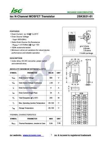
isc N-Channel MOSFET Transistor 2SK3531-01 FEATURES Drain Current I = 6A@ T =25 D C Drain Source Voltage V = 900V(Min) DSS Static Drain-Source On-Resistance R = 2.5 (Max) @ V = 10V DS(on) GS 100% avalanche tested Minimum Lot-to-Lot variations for robust device performance and reliable operation DESCRIPTION motor drive, DC-DC converter, power switch and solen
8.13. Size:280K inchange semiconductor
2sk3532-01mr.pdf 
isc N-Channel MOSFET Transistor 2SK3532-01MR FEATURES Drain Current I = 6A@ T =25 D C Drain Source Voltage V = 900V(Min) DSS Static Drain-Source On-Resistance R = 2.5 (Max) @ V = 10V DS(on) GS 100% avalanche tested Minimum Lot-to-Lot variations for robust device performance and reliable operation DESCRIPTION motor drive, DC-DC converter, power switch and sol
8.14. Size:280K inchange semiconductor
2sk3534-01mr.pdf 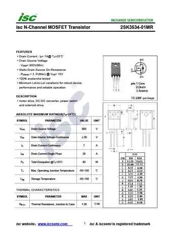
isc N-Channel MOSFET Transistor 2SK3534-01MR FEATURES Drain Current I = 7A@ T =25 D C Drain Source Voltage V = 900V(Min) DSS Static Drain-Source On-Resistance R = 2. (Max) @ V = 10V DS(on) GS 100% avalanche tested Minimum Lot-to-Lot variations for robust device performance and reliable operation DESCRIPTION motor drive, DC-DC converter, power switch and sole
8.15. Size:280K inchange semiconductor
2sk3537-01mr.pdf 
isc N-Channel MOSFET Transistor 2SK3537-01MR FEATURES Drain Current I = 23A@ T =25 D C Drain Source Voltage V = 150V(Min) DSS Static Drain-Source On-Resistance R = 70m (Max) @ V = 10V DS(on) GS 100% avalanche tested Minimum Lot-to-Lot variations for robust device performance and reliable operation DESCRIPTION motor drive, DC-DC converter, power switch and so
Другие MOSFET... ITF87068SQT
, ITF87072DK8T
, 12N65KL-TF
, 20N03
, 2N0609
, 2SK2080
, 2SK2652
, 2SK2654
, IRFP450
, 2SK3681
, 3N150S
, 80N08A
, AOB12N65
, AOB2144L
, IXFH10N100
, IXFH10N90
, IXFH11N80
.
History: NTD20N06LT4G
| VS4020AS
| IXFN150N15
| 2P903V
| 2SK1380
| SQD40N06-14
| KI30P03DFN
