ST2303SRG. Аналоги и основные параметры
Наименование производителя: ST2303SRG
Тип транзистора: MOSFET
Полярность: P
Предельные значения
Pd ⓘ
- Максимальная рассеиваемая мощность: 1.25 W
|Vds|ⓘ - Максимально допустимое напряжение сток-исток: 30 V
|Vgs|ⓘ - Максимально допустимое напряжение затвор-исток: 20 V
|Id| ⓘ - Максимально допустимый постоянный ток стока: 2.6 A
Tj ⓘ - Максимальная температура канала: 150 °C
Электрические характеристики
tr ⓘ -
Время нарастания: 9 ns
Cossⓘ - Выходная емкость: 87 pf
RDSonⓘ - Сопротивление сток-исток открытого транзистора: 0.095 Ohm
Тип корпуса: SOT-23
Аналог (замена) для ST2303SRG
- подборⓘ MOSFET транзистора по параметрам
ST2303SRG даташит
..1. Size:200K stansontech
st2303srg.pdf 

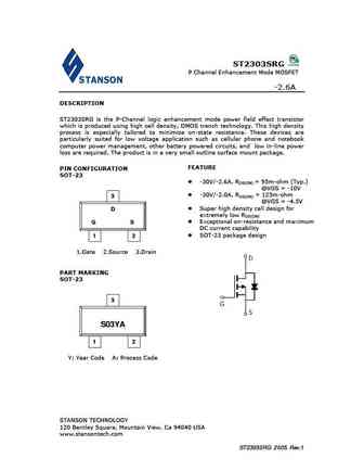
ST2303SRG P Channel Enhancement Mode MOSFET -2.6A DESCRIPTION ST2303SRG is the P-Channel logic enhancement mode power field effect transistor which is produced using high cell density, DMOS trench technology. This high density process is especially tailored to minimize on-state resistance. These devices are particularly suited for low voltage application such as cellular phone a
8.1. Size:1367K winsok
wst2303a.pdf 

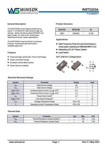
WST2303A P-Ch MOSFET General Description Product Summery The WST2303A is the highest performance BVDSS RDSON ID trench P-ch MOSFET with extreme high cell density , which provide excellent RDSON and -20V 144m -2.5A gate charge for most of the small power switching and load switch applications. Applications The WST2303A meet the RoHS and Green Product requirement with full
8.2. Size:1058K winsok
wst2303.pdf 

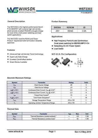
WST2303 P-Ch MOSFET General Description Product Summery The WST2303 is the highest performance trench BVDSS RDSON ID P-Ch MOSFET with extreme high cell density , which provide excellent RDSON and gate charge -20V 65m -3.8A for most of the small power switching and load switch applications. Applications The WST2303 meet the RoHS and Green High Frequency Point-of-Load
9.1. Size:212K stansontech
st2305.pdf 

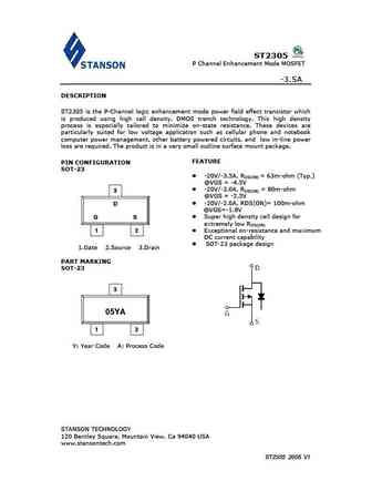
ST2305 P Channel Enhancement Mode MOSFET -3.5A DESCRIPTION ST2305 is the P-Channel logic enhancement mode power field effect transistor which is produced using high cell density, DMOS trench technology. This high density process is especially tailored to minimize on-state resistance. These devices are particularly suited for low voltage application such as cellular phone and not
9.2. Size:383K stansontech
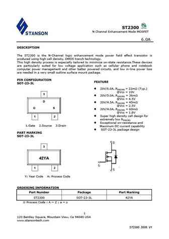
st2300.pdf 

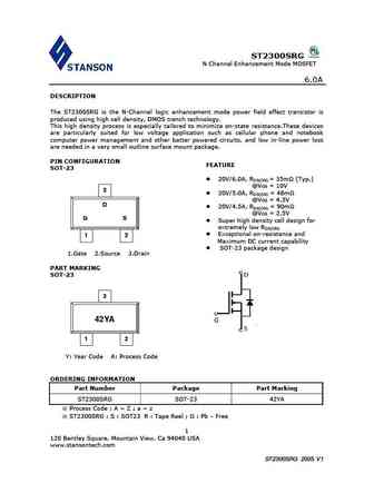
ST2300 N Channel Enhancement Mode MOSFET 6.0A DESCRIPTION The ST2300 is the N-Channel logic enhancement mode power field effect transistor is produced using high cell density, DMOS trench technology. This high density process is especially tailored to minimize on-state resistance.These devices are particularly suited for low voltage application such as cellular phone and noteboo
9.3. Size:188K stansontech
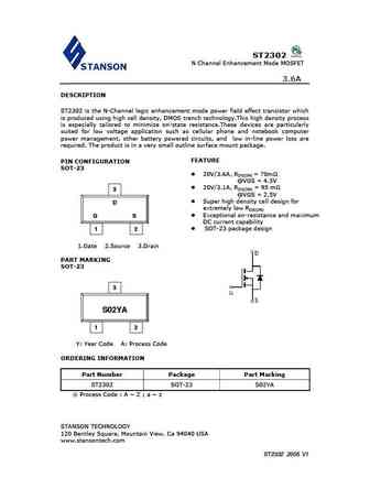
st2302.pdf 

ST2302 N Channel Enhancement Mode MOSFET 3.6A DESCRIPTION ST2302 is the N-Channel logic enhancement mode power field effect transistor which is produced using high cell density, DMOS trench technology.This high density process is especially tailored to minimize on-state resistance.These devices are particularly suited for low voltage application such as cellular phone and noteboo
9.4. Size:161K stansontech
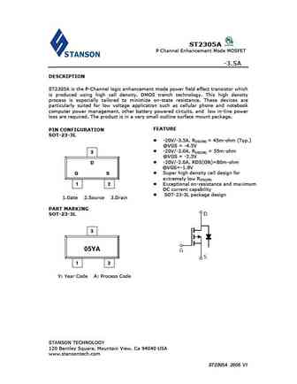
st2305a.pdf 

ST2305A P Channel Enhancement Mode MOSFET -3.5A DESCRIPTION ST2305A is the P-Channel logic enhancement mode power field effect transistor which is produced using high cell density, DMOS trench technology. This high density process is especially tailored to minimize on-state resistance. These devices are particularly suited for low voltage application such as cellular phone and no
9.5. Size:753K stansontech
st2304srg.pdf 

ST2304SRG N Channel Enhancement Mode MOSFET 3.2A DESCRIPTION ST2304SRG is the N-Channel logic enhancement mode power field effect transistor which is produced using high cell density, DMOS trench technology. This high density process is especially tailored to minimize on-state resistance. These devices are particularly suited for low voltage application such as cellular phone an
9.6. Size:897K stansontech
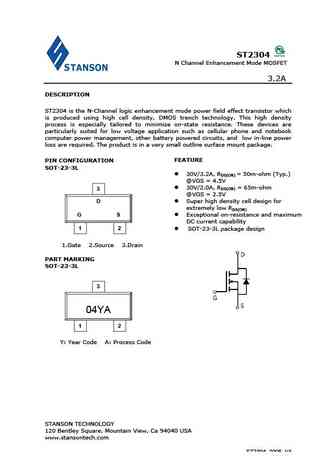
st2304.pdf 

ST2304 N Channel Enhancement Mode MOSFET 3.2A DESCRIPTION ST2304 is the N-Channel logic enhancement mode power field effect transistor which is produced using high cell density, DMOS trench technology. This high density process is especially tailored to minimize on-state resistance. These devices are particularly suited for low voltage application such as cellular phone and note
9.7. Size:479K stansontech
st2300srg.pdf 

ST2300SRG N Channel Enhancement Mode MOSFET 6.0A DESCRIPTION The ST2300SRG is the N-Channel logic enhancement mode power field effect transistor is produced using high cell density, DMOS trench technology. This high density process is especially tailored to minimize on-state resistance.These devices are particularly suited for low voltage application such as cellular phone and n
9.8. Size:187K stansontech
st2301a.pdf 

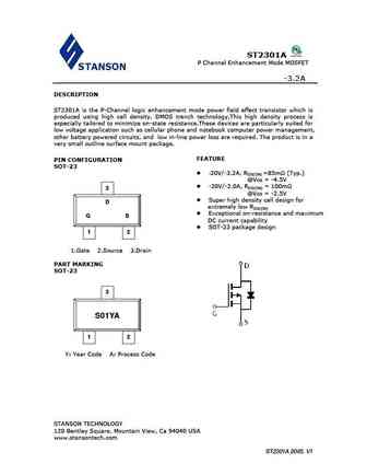
ST2301A P Channel Enhancement Mode MOSFET -3.2A DESCRIPTION ST2301A is the P-Channel logic enhancement mode power field effect transistor which is produced using high cell density, DMOS trench technology.This high density process is especially tailored to minimize on-state resistance.These devices are particularly suited for low voltage application such as cellular phone and not
9.9. Size:1440K jestek
jst2300.pdf 

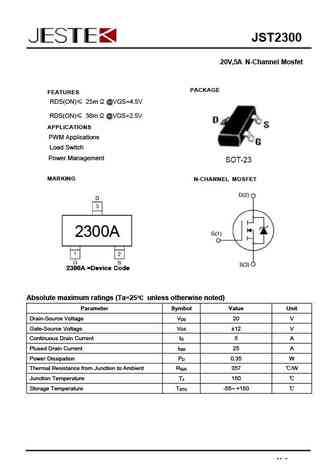
JST2300 20V,5A N-Channel Mosfet PACKAGE FEATURES RDS(ON) 25m @VGS=4.5V RDS(ON) 38m @VGS=2.5V APPLICATIONS PWM Applications Load Switch Power Management MARKING N-CHANNEL MOSFET Absolute maximum ratings (Ta=25 unless otherwise noted) Parameter Symbol Value Unit Drain-Source Voltage V 20 V DS Gate-Source Voltage V 12 V GS Continuous Drain Current I 5 A D Pl
9.10. Size:592K jestek
jst2301h.pdf 

JST2301H -20V,-3A P-Channel Mosfet FEATURES SOT-23 RDS(ON) 110m @VGS=-4.5V RDS(ON) 140m @VGS=-2.5V APPLICATIONS Load Switch for Portable Devices DC/DC Converter MARKING P-CHANNEL MOSFET Maximum ratings (Ta=25 unless otherwise noted) Parameter Symbol Value Unit Drain-Source Voltage VDS -20 V Gate-Source Voltage V 12 GS I -3 D Continuous Drain Current A Pulse
9.11. Size:583K jestek
jst2302h.pdf 

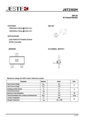
JST2302H 20V,3A N-Channel Mosfet FEATURES SOT-23 RDS(ON) 46m @VGS=4.5V RDS(ON) 70m @VGS=2.5V APPLICATIONS Load Switch for Portable Devices DC/DC Converter MARKING N-CHANNEL MOSFET Maximum ratings (Ta=25 unless otherwise noted) Parameter Symbol Value Unit Drain-Source Voltage VDS 20 V Gate-Source Voltage V 10 GS I 3 D Continuous Drain Current A Pulsed Drain
9.12. Size:888K winsok
wst2301.pdf 

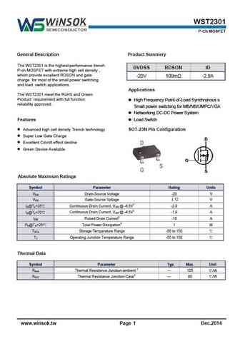
WST2301 P-Ch MOSFET General Description Product Summery The WST2301 is the highest performance trench BVDSS RDSON ID P-ch MOSFET with extreme high cell density , which provide excellent RDSON and gate -20V 100m -2.9A charge for most of the small power switching and load switch applications. Applications The WST2301 meet the RoHS and Green Product requirement with full fu
9.13. Size:1269K winsok
wst2304.pdf 

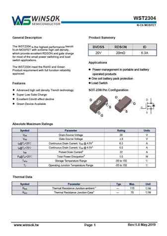
WST2304 N-Ch MOSFET General Description Product Summery The WST2304 is the highest performance trench BVDSS RDSON ID N-ch MOSFET with extreme high cell density , 20V 20m 6.3A which provide excellent RDSON and gate charge for most of the small power switching and load switch applications. Applications The WST2304 meet the RoHS and Green Power management in portable and
9.14. Size:980K winsok
wst2300.pdf 

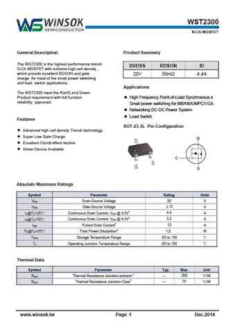
WST2300 N-Ch MOSFET General Description Product Summery The WST2300 is the highest performance trench BVDSS RDSON ID N-Ch MOSFET with extreme high cell density , which provide excellent RDSON and gate 20V 50m 4.4A charge for most of the small power switching and load switch applications. Applications The WST2300 meet the RoHS and Green Product requirement with full funct
9.15. Size:1367K winsok
wst2302.pdf 

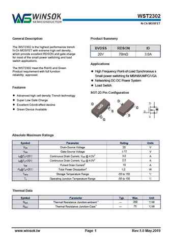
WST2302 N-Ch MOSFET General Description Product Summery The WST2302 is the highest performance trench BVDSS RDSON ID N-Ch MOSFET with extreme high cell density , which provide excellent RDSON and gate charge 20V 70m 3.0A for most of the small power switching and load switch applications. Applications The WST2302 meet the RoHS and Green Product requirement with full functio
9.16. Size:1740K winsok
wst2307.pdf 

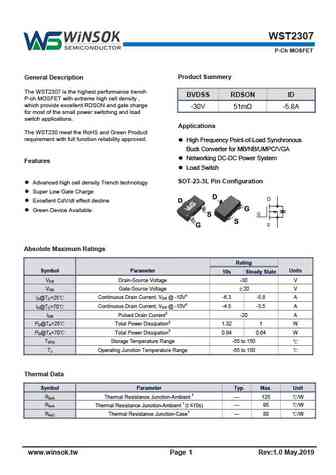
WST2307 P-Ch MOSFET Product Summery General Description The WST2307 is the highest performance trench BVDSS RDSON ID P-ch MOSFET with extreme high cell density , which provide excellent RDSON and gate charge -30V 51m -5.8A for most of the small power switching and load switch applications. Applications The WST230 meet the RoHS and Green Product requirement with full functio
9.17. Size:1114K winsok
wst2301a.pdf 

WST2301A P-Ch MOSFET General Description Product Summery The WST2301A is the highest performance BVDSS RDSON ID trench P-ch MOSFET with extreme high cell density , which provide excellent RDSON and -20V 140m -2.5A gate charge for most of the small power switching and load switch applications. Applications The WST2301A meet the RoHS and Green Product requirement with full
9.18. Size:1208K winsok
wst2300a.pdf 

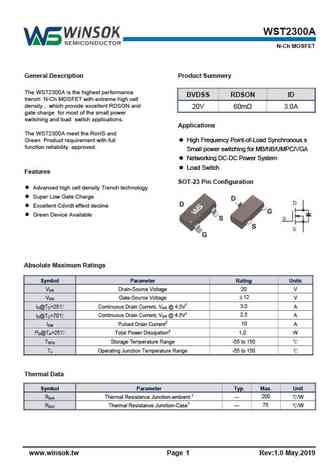
WST2300A N-Ch MOSFET General Description Product Summery The WST2300A is the highest performance BVDSS RDSON ID trench N-Ch MOSFET with extreme high cell density , which provide excellent RDSON and 20V 60m 3.0A gate charge for most of the small power switching and load switch applications. Applications The WST2300A meet the RoHS and Green Product requirement with full
9.19. Size:1337K winsok
wst2304a.pdf 

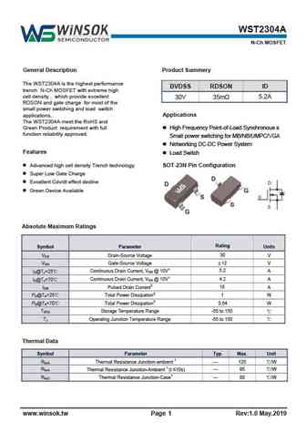
WST2304A N-Ch MOSFET General Description Product Summery The WST2304A is the highest performance BVDSS RDSON ID trench N-Ch MOSFET with extreme high cell density , which provide excellent 30V 35m 5.2A RDSON and gate charge for most of the small power switching and load switch Applications applications. The WST2304A meet the RoHS and Green Product requirement with full
9.20. Size:1613K winsok
wst2305a.pdf 

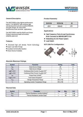
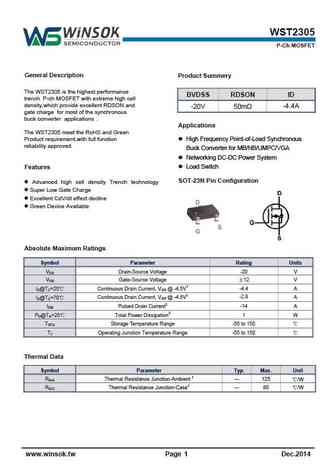
WST2305A P-Ch MOSFET General Description Product Summery The WST2305A is the highest performance BVDSS RDSON ID trench P-ch MOSFET with extreme high cell density,which provide excellent RDSON -4A -20V 60m and gate charge for most of the synchronous buck converter applications . Applications The WST2305A meet the RoHS and Green Product requirement,with full function Hi
9.21. Size:951K winsok
wst2305.pdf 

WST2305 P-Ch MOSFET General Description Product Summery The WST2305 is the highest performance BVDSS RDSON ID trench P-ch MOSFET with extreme high cell density,which provide excellent RDSON and -4.4A -20V 50m gate charge for most of the synchronous buck converter applications . Applications The WST2305 meet the RoHS and Green Product requirement,with full function H
9.22. Size:878K cn vbsemi
st2302.pdf 

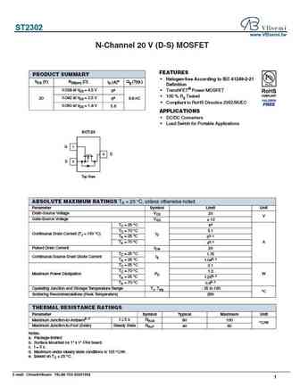
ST2302 www.VBsemi.tw N-Channel 20 V (D-S) MOSFET FEATURES PRODUCT SUMMARY Halogen-free According to IEC 61249-2-21 VDS (V) RDS(on) ( ) ID (A)e Qg (Typ.) Definition 0.028 at VGS = 4.5 V TrenchFET Power MOSFET 6a 100 % Rg Tested 20 0.042 at VGS = 2.5 V 6a 8.8 nC Compliant to RoHS Directive 2002/95/EC 0.050 at VGS = 1.8 V 5.6 APPLICATIONS DC/DC Co
9.23. Size:848K cn vbsemi
st2304.pdf 

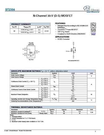
ST2304 www.VBsemi.tw N-Channel 30-V (D-S) MOSFET FEATURES PRODUCT SUMMARY Halogen-free According to IEC 61249-2-21 VDS (V) RDS(on) ( ) ID (A)a Qg (Typ.) Definition 0.030 at VGS = 10 V TrenchFET Power MOSFET 6.5 30 4.5 nC 100 % Rg Tested 0.033 at VGS = 4.5 V 6.0 Compliant to RoHS Directive 2002/95/EC APPLICATIONS DC/DC Converter D TO-236 (SOT-23) G 1
9.24. Size:919K cn vbsemi
st2302msrg.pdf 

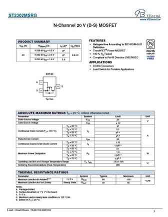
ST2302MSRG www.VBsemi.tw N-Channel 20 V (D-S) MOSFET FEATURES PRODUCT SUMMARY Halogen-free According to IEC 61249-2-21 VDS (V) RDS(on) ( ) ID (A)e Qg (Typ.) Definition 0.028 at VGS = 4.5 V TrenchFET Power MOSFET 6a 100 % Rg Tested 20 0.042 at VGS = 2.5 V 6a 8.8 nC Compliant to RoHS Directive 2002/95/EC 0.050 at VGS = 1.8 V 5.6 APPLICATIONS DC/D
9.25. Size:878K cn vbsemi
st2300s23rg.pdf 

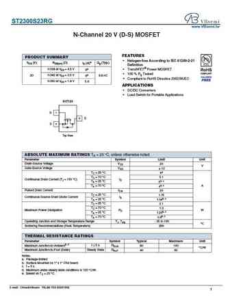
ST2300S23RG www.VBsemi.tw N-Channel 20 V (D-S) MOSFET FEATURES PRODUCT SUMMARY Halogen-free According to IEC 61249-2-21 VDS (V) RDS(on) ( ) ID (A)e Qg (Typ.) Definition 0.028 at VGS = 4.5 V TrenchFET Power MOSFET 6a 100 % Rg Tested 20 0.042 at VGS = 2.5 V 6a 8.8 nC Compliant to RoHS Directive 2002/95/EC 0.050 at VGS = 1.8 V 5.6 APPLICATIONS DC/
Другие IGBT... ST1005SRG, ST10E4, ST12N10D, ST13P10, ST2300, ST2300SRG, ST2301A, ST2302, 10N60, ST2304, ST2304SRG, ST2305, ST2305A, ST2318SRG, ST2319SRG, ST2341A, ST2341S23RG
