J110. Аналоги и основные параметры
Наименование производителя: J110
Тип транзистора: JFET
Полярность: N
Предельные значения
Pd ⓘ
- Максимальная рассеиваемая мощность: 0.4 W
|Vds|ⓘ - Максимально допустимое напряжение сток-исток: 25 V
|Id| ⓘ - Максимально допустимый постоянный ток стока: 0.01 A
Tj ⓘ - Максимальная температура канала: 150 °C
Электрические характеристики
Cossⓘ - Выходная емкость: 15 pf
RDSonⓘ - Сопротивление сток-исток открытого транзистора: 18 Ohm
Тип корпуса: TO92
- подборⓘ MOSFET транзистора по параметрам
J110 даташит
..1. Size:45K philips
j108 j109 j110 1.pdf 

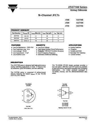
DISCRETE SEMICONDUCTORS DATA SHEET J108; J109; J110 N-channel silicon junction FETs Product specification 1996 Jul 30 Supersedes data of April 1995 File under Discrete Semiconductors, SC07 Philips Semiconductors Product specification N-channel silicon junction FETs J108; J109; J110 FEATURES PINNING - TO-92 High speed switching PIN SYMBOL DESCRIPTION Interchangeability of dr
..2. Size:129K fairchild semi
j108 j109 j110 mmbfj108.pdf 
J108/J109/J110/MMBFJ108 N-Channel Switch 3 This device is designed for digital switching applications where very low on resistance is mandatory. 2 Sourced from Process 58. TO-92 1 SuperSOT-3 1 Marking I8 1. Drain 2. Source 3. Gate 1. Drain 2. Source 3. Gate Absolute Maximum Ratings * TA=25 C unless otherwise noted Symbol Parameter Value Units VDG Drain-Gate Voltage 25
0.1. Size:235K motorola
mj11017-18 21-22 mj11017r.pdf 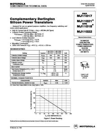
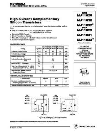
Order this document MOTOROLA by MJ11017/D SEMICONDUCTOR TECHNICAL DATA PNP MJ11017 Complementary Darlington MJ11021* Silicon Power Transistors NPN . . . designed for use as general purpose amplifiers, low frequency switching and MJ11018* motor control applications. High dc Current Gain @ 10 Adc hFE = 400 Min (All Types) MJ11022 Collector Emitter Sustaining Voltage
0.3. Size:157K motorola
mj11012r.pdf 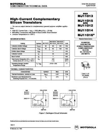
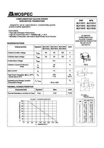
Order this document MOTOROLA by MJ11012/D SEMICONDUCTOR TECHNICAL DATA PNP MJ11013 High-Current Complementary MJ11015 Silicon Transistors NPN MJ11012 . . . for use as output devices in complementary general purpose amplifier applica- tions. High DC Current Gain hFE = 1000 (Min) @ IC 20 Adc MJ11014 Monolithic Construction with Built in Base Emitter Shunt Resistor
0.4. Size:34K philips
j108-j109-j110.pdf 
DISCRETE SEMICONDUCTORS DATA SHEET J108; J109; J110 N-channel silicon junction FETs Product specification 1996 Jul 30 Supersedes data of April 1995 File under Discrete Semiconductors, SC07 Philips Semiconductors Product specification N-channel silicon junction FETs J108; J109; J110 FEATURES PINNING - TO-92 High speed switching PIN SYMBOL DESCRIPTION Interchangeability of dr
0.5. Size:32K philips
pmbfj108 pmbfj109 pmbfj110 cnv 2.pdf 
DISCRETE SEMICONDUCTORS DATA SHEET PMBFJ108; PMBFJ109; PMBFJ110 N-channel junction FETs April 1995 Product specification File under Discrete Semiconductors, SC07 Philips Semiconductors Product specification PMBFJ108; N-channel junction FETs PMBFJ109; PMBFJ110 FEATURES High-speed switching Interchangeability of drain and source connections Low RDSon at zero gate volt
0.6. Size:46K philips
pmbfj108 pmbfj109 pmbfj110.pdf 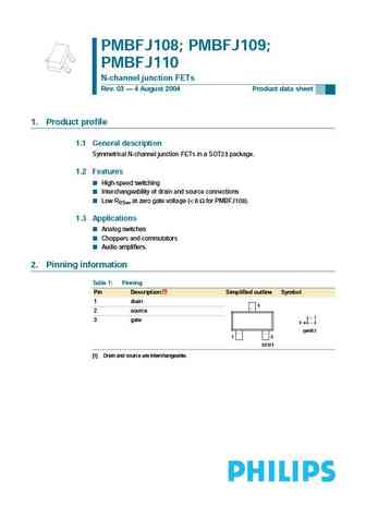
PMBFJ108; PMBFJ109; PMBFJ110 N-channel junction FETs Rev. 03 4 August 2004 Product data sheet 1. Product profile 1.1 General description Symmetrical N-channel junction FETs in a SOT23 package. 1.2 Features High-speed switching Interchangeability of drain and source connections Low RDSon at zero gate voltage (
0.7. Size:147K toshiba
ssm3j110tu.pdf 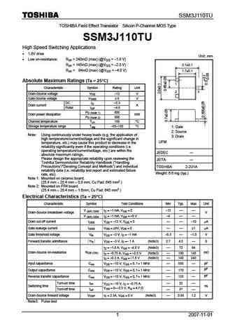
SSM3J110TU TOSHIBA Field Effect Transistor Silicon P-Channel MOS Type SSM3J110TU High Speed Switching Applications 1.8V drive Unit mm Low on-resistance Ron = 240m (max) (@VGS = -1.8 V) Ron = 145m (max) (@VGS = -2.5 V) 2.1 0.1 Ron = 94m (max) (@VGS = -4.0 V) 1.7 0.1 Absolute Maximum Ratings (Ta = 25 C) 1 Characteristic Symbol Rating Unit 3 2 Drain-Sou
0.8. Size:178K fairchild semi
mmbfj110.pdf 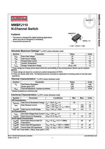
April 2011 MMBFJ110 N-Channel Switch SuperSOT-3 Features 3 This device is designed for digital switching applications 2 where very low on resistance is mandatory. Marking 110 Sourced from process 58. 1 1. Drain 2. Source 3. Gate Absolute Maximum Ratings* TA=25 C unless otherwise noted Symbol Parameter Value Units VDG Drain-Gate Voltage 25 V VGS Gate-Source Voltage -
0.9. Size:52K onsemi
j110-d.pdf 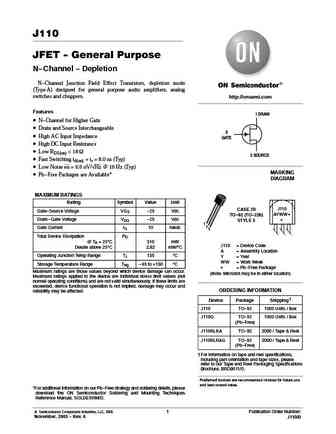
J110 JFET - General Purpose N-Channel - Depletion N-Channel Junction Field Effect Transistors, depletion mode (Type A) designed for general purpose audio amplifiers, analog switches and choppers. http //onsemi.com Features 1 DRAIN N-Channel for Higher Gain Drain and Source Interchangeable 3 High AC Input Impedance GATE High DC Input Resistance Low RDS(on)
0.10. Size:116K onsemi
mj11032g.pdf 
MJ11028, MJ11030, MJ11032 (NPN) MJ11029, MJ11033 (PNP) High-Current Complementary Silicon http //onsemi.com Power Transistors High-Current Complementary Silicon Power Transistors are for use 50 AMPERE as output devices in complementary general purpose amplifier COMPLEMENTARY applications. DARLINGTON POWER Features TRANSISTORS High DC Current Gain - hFE = 1000 (Min) @ IC = 25
0.11. Size:127K onsemi
mj11022g.pdf 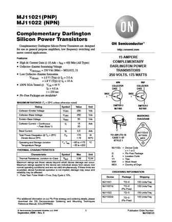
MJ11021(PNP) MJ11022 (NPN) Complementary Darlington Silicon Power Transistors Complementary Darlington Silicon Power Transistors are designed for use as general purpose amplifiers, low frequency switching and http //onsemi.com motor control applications. 15 AMPERE Features COMPLEMENTARY High dc Current Gain @ 10 Adc - hFE = 400 Min (All Types) DARLINGTON POWER Collector-Emi
0.12. Size:116K onsemi
mj11033g.pdf 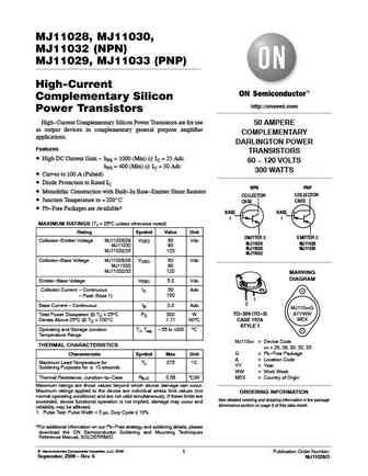
MJ11028, MJ11030, MJ11032 (NPN) MJ11029, MJ11033 (PNP) High-Current Complementary Silicon http //onsemi.com Power Transistors High-Current Complementary Silicon Power Transistors are for use 50 AMPERE as output devices in complementary general purpose amplifier COMPLEMENTARY applications. DARLINGTON POWER Features TRANSISTORS High DC Current Gain - hFE = 1000 (Min) @ IC = 25
0.13. Size:116K onsemi
mj11028g.pdf 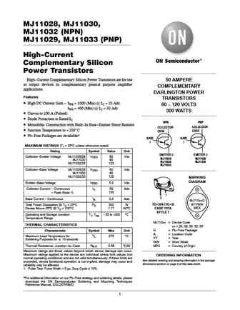
MJ11028, MJ11030, MJ11032 (NPN) MJ11029, MJ11033 (PNP) High-Current Complementary Silicon Power Transistors High-Current Complementary Silicon Power Transistors are for use 50 AMPERE as output devices in complementary general purpose amplifier COMPLEMENTARY applications. DARLINGTON POWER Features TRANSISTORS High DC Current Gain - hFE = 1000 (Min) @ IC = 25 Adc 60 - 120 VOLTS
0.14. Size:116K onsemi
mj11012g.pdf 
MJ11015 (PNP); MJ11012, MJ11016 (NPN) MJ11016 is a Preferred Device High-Current Complementary Silicon Transistors http //onsemi.com . . . for use as output devices in complementary general purpose amplifier applications. 30 AMPERE DARLINGTON High DC Current Gain - POWER TRANSISTORS hFE = 1000 (Min) @ IC - 20 Adc COMPLEMENTARY SILICON Monolithic Construction with Built-in
0.15. Size:116K onsemi
mj11016g.pdf 
MJ11015 (PNP); MJ11012, MJ11016 (NPN) MJ11016 is a Preferred Device High-Current Complementary Silicon Transistors http //onsemi.com . . . for use as output devices in complementary general purpose amplifier applications. 30 AMPERE DARLINGTON High DC Current Gain - POWER TRANSISTORS hFE = 1000 (Min) @ IC - 20 Adc COMPLEMENTARY SILICON Monolithic Construction with Built-in
0.16. Size:127K onsemi
mj11021g.pdf 
MJ11021(PNP) MJ11022 (NPN) Complementary Darlington Silicon Power Transistors Complementary Darlington Silicon Power Transistors are designed for use as general purpose amplifiers, low frequency switching and http //onsemi.com motor control applications. 15 AMPERE Features COMPLEMENTARY High dc Current Gain @ 10 Adc - hFE = 400 Min (All Types) DARLINGTON POWER Collector-Emi
0.17. Size:116K onsemi
mj11015g.pdf 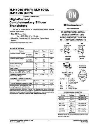
MJ11015 (PNP); MJ11012, MJ11016 (NPN) MJ11016 is a Preferred Device High-Current Complementary Silicon Transistors http //onsemi.com . . . for use as output devices in complementary general purpose amplifier applications. 30 AMPERE DARLINGTON High DC Current Gain - POWER TRANSISTORS hFE = 1000 (Min) @ IC - 20 Adc COMPLEMENTARY SILICON Monolithic Construction with Built-in
0.19. Size:171K cdil
mj11015 6.pdf 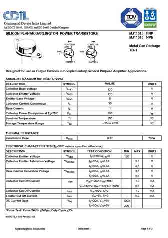
Continental Device India Limited An ISO/TS 16949, ISO 9001 and ISO 14001 Certified Company MJ11015 PNP SILICON PLANAR DARLINGTON POWER TRANSISTORS MJ11016 NPN Metal Can Package TO-3 Designed for use as Output Devices in Complementary General Purpose Amplifier Applications. ABSOLUTE MAXIMUM RATINGS (Ta=25 C) DESCRIPTION SYMBOL VALUE UNITS Collector Base Voltage VCBO V 120 Collector
0.20. Size:432K cn vbsemi
vbj1101m.pdf 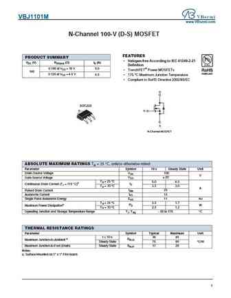
VBJ1101M www.VBsemi.com N-Channel 100-V (D-S) MOSFET FEATURES PRODUCT SUMMARY Halogen-free According to IEC 61249-2-21 VDS (V) RDS(on) ( )ID (A) Definition 0.100 at VGS = 10 V 5.0 TrenchFET Power MOSFETs 100 0.120 at VGS = 4.5 V 4.5 175 C Maximum Junction Temperature Compliant to RoHS Directive 2002/95/EC D SOT-223 D G S D G S N-Channel MOSFET
0.21. Size:207K inchange semiconductor
mj11030.pdf 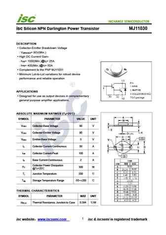
isc Silicon NPN Darlington Power Transistor MJ11030 DESCRIPTION Collector-Emitter Breakdown Voltage V = 90V(Min.) (BR)CEO High DC Current Gain- h = 1000(Min.)@I = 25A FE C h = 400(Min.)@I = 50A FE C Complement to the PNP MJ11031 Minimum Lot-to-Lot variations for robust device performance and reliable operation APPLICATIONS Designed for use as output devices in comp
0.22. Size:207K inchange semiconductor
mj11032.pdf 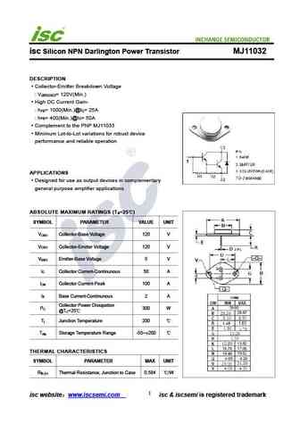
isc Silicon NPN Darlington Power Transistor MJ11032 DESCRIPTION Collector-Emitter Breakdown Voltage V = 120V(Min.) (BR)CEO High DC Current Gain- h = 1000(Min.)@I = 25A FE C h = 400(Min.)@I = 50A FE C Complement to the PNP MJ11033 Minimum Lot-to-Lot variations for robust device performance and reliable operation APPLICATIONS Designed for use as output devices in com
0.23. Size:212K inchange semiconductor
mj11017.pdf 
isc Silicon PNP Darlington Power Transistor MJ11017 DESCRIPTION High DC Current Gain- h = 400(Min)@ I = -10A FE C Collector-Emitter Sustaining Voltage- V = -150V(Min) CEO(SUS) Low Collector-Emitter Saturation Voltage- V = -2.0V(Max)@ I = -10A CE(sat) C = -3.4V(Max)@ I = -15A C Complement to the NPN MJ11018 Minimum Lot-to-Lot variations for robust device performanc
0.24. Size:212K inchange semiconductor
mj11018.pdf 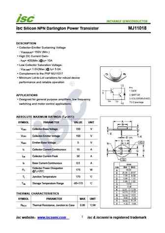
isc Silicon NPN Darlington Power Transistor MJ11018 DESCRIPTION Collector-Emitter Sustaining Voltage V = 150V (Min.) CEO(SUS) High DC Current Gain- h = 400(Min.)@I = 10A FE C Low Collector Saturation Voltage- V = 1.0V(Max.)@ I = 5.0A CE (sat) C Complement to the PNP MJ11017 Minimum Lot-to-Lot variations for robust device performance and reliable operation APPLICATI
0.25. Size:208K inchange semiconductor
mj11013.pdf 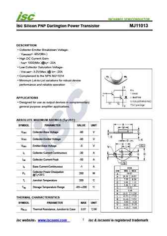
isc Silicon PNP Darlington Power Transistor MJ11013 DESCRIPTION Collector-Emitter Breakdown Voltage- V = -90V(Min.) (BR)CEO High DC Current Gain- h = 1000(Min.)@I = -20A FE C Low Collector Saturation Voltage- V = -3.0V(Max.)@ I = -20A CE (sat) C Complement to the NPN MJ11014 Minimum Lot-to-Lot variations for robust device performance and reliable operation APPLICAT
0.26. Size:208K inchange semiconductor
mj11031.pdf 
isc Silicon PNP Darlington Power Transistor MJ11031 DESCRIPTION Collector-Emitter Breakdown Voltage V = -90V(Min.) (BR)CEO High DC Current Gain- h = 1000(Min.)@I = -25A FE C h = 400(Min.)@I = -50A FE C Complement to the NPN MJ11030 Minimum Lot-to-Lot variations for robust device performance and reliable operation APPLICATIONS Designed for use as output devices in c
0.27. Size:208K inchange semiconductor
mj11028.pdf 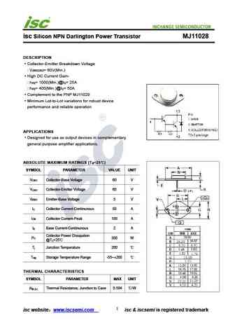
isc Silicon NPN Darlington Power Transistor MJ11028 DESCRIPTION Collector-Emitter Breakdown Voltage V = 60V(Min.) (BR)CEO High DC Current Gain- h = 1000(Min.)@I = 25A FE C h = 400(Min.)@I = 50A FE C Complement to the PNP MJ11029 Minimum Lot-to-Lot variations for robust device performance and reliable operation APPLICATIONS Designed for use as output devices in comp
0.28. Size:211K inchange semiconductor
mj11019.pdf 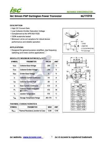
isc Silicon PNP Darlington Power Transistor MJ11019 DESCRIPTION High DC Current Gain Low Collector-Emitter Saturation Voltage Complement to the NPN MJ11020 100% avalanche tested Minimum Lot-to-Lot variations for robust device performance and reliable operation APPLICATIONS Designed for general purpose amplifiers ,low frequency switching and motor control applications. ABS
0.29. Size:208K inchange semiconductor
mj11022.pdf 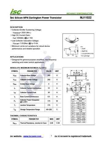
isc Silicon NPN Darlington Power Transistor MJ11022 DESCRIPTION Collector-Emitter Sustaining Voltage- V = 250V (Min.) CEO(SUS) High DC Current Gain- h = 400(Min.)@I = 10A FE C Low Collector Saturation Voltage- V = 1.0V(Max.)@ I = 5.0A CE (sat) C Minimum Lot-to-Lot variations for robust device performance and reliable operation APPLICATIONS Designed for general purp
0.30. Size:207K inchange semiconductor
mj11029.pdf 
isc Silicon PNP Darlington Power Transistor MJ11029 DESCRIPTION Collector-Emitter Breakdown Voltage V = -60V(Min.) (BR)CEO High DC Current Gain- h = 1000(Min.)@I = -25A FE C h = 400(Min.)@I = -50A FE C Complement to the NPN MJ11028 Minimum Lot-to-Lot variations for robust device performance and reliable operation APPLICATIONS Designed for use as output devices in c
0.31. Size:208K inchange semiconductor
mj11020.pdf 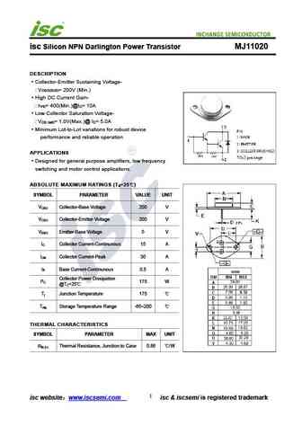
isc Silicon NPN Darlington Power Transistor MJ11020 DESCRIPTION Collector-Emitter Sustaining Voltage- V = 200V (Min.) CEO(SUS) High DC Current Gain- h = 400(Min.)@I = 10A FE C Low Collector Saturation Voltage- V = 1.0V(Max.)@ I = 5.0A CE (sat) C Minimum Lot-to-Lot variations for robust device performance and reliable operation APPLICATIONS Designed for general purp
0.32. Size:51K inchange semiconductor
mj11016.pdf 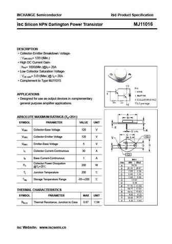
INCHANGE Semiconductor isc Product Specification isc Silicon NPN Darlington Power Transistor MJ11016 DESCRIPTION Collector-Emitter Breakdown Voltage- V(BR)CEO= 120V(Min.) High DC Current Gain- hFE= 1000(Min.)@IC= 20A Low Collector Saturation Voltage- VCE (sat)= 3.0V(Max.)@ IC= 20A Complement to Type MJ11015 APPLICATIONS Designed for use as output devices
0.33. Size:208K inchange semiconductor
mj11015.pdf 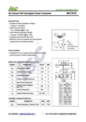
isc Silicon PNP Darlington Power Transistor MJ11015 DESCRIPTION Collector-Emitter Breakdown Voltage- V = -120V(Min.) (BR)CEO High DC Current Gain- h = 1000(Min.)@I = -20A FE C Low Collector Saturation Voltage- V = -3.0V(Max.)@ I = -20A CE (sat) C Complement to the NPN MJ11016 Minimum Lot-to-Lot variations for robust device performance and reliable operation APPLICA
0.34. Size:207K inchange semiconductor
mj11014.pdf 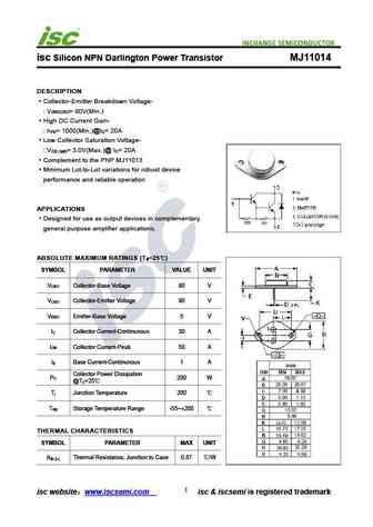
isc Silicon NPN Darlington Power Transistor MJ11014 DESCRIPTION Collector-Emitter Breakdown Voltage- V = 90V(Min.) (BR)CEO High DC Current Gain- h = 1000(Min.)@I = 20A FE C Low Collector Saturation Voltage- V = 3.0V(Max.)@ I = 20A CE (sat) C Complement to the PNP MJ11013 Minimum Lot-to-Lot variations for robust device performance and reliable operation APPLICATIONS
0.35. Size:207K inchange semiconductor
mj11012.pdf 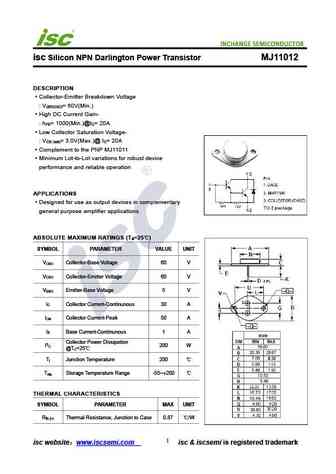
isc Silicon NPN Darlington Power Transistor MJ11012 DESCRIPTION Collector-Emitter Breakdown Voltage V = 60V(Min.) (BR)CEO High DC Current Gain- h = 1000(Min.)@I = 20A FE C Low Collector Saturation Voltage- V = 3.0V(Max.)@ I = 20A CE (sat) C Complement to the PNP MJ11011 Minimum Lot-to-Lot variations for robust device performance and reliable operation APPLICATIONS
0.36. Size:53K inchange semiconductor
mj11033.pdf 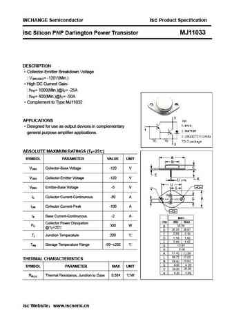
INCHANGE Semiconductor isc Product Specification isc Silicon PNP Darlington Power Transistor MJ11033 DESCRIPTION Collector-Emitter Breakdown Voltage V(BR)CEO= -120V(Min.) High DC Current Gain- hFE= 1000(Min.)@IC= -25A hFE= 400(Min.)@IC= -50A Complement to Type MJ11032 APPLICATIONS Designed for use as output devices in complementary general purpose amplifie
0.37. Size:207K inchange semiconductor
mj11011.pdf 
isc Silicon PNP Darlington Power Transistor MJ11011 DESCRIPTION Collector-Emitter Breakdown Voltage V = -60V(Min.) (BR)CEO High DC Current Gain- h = 1000(Min.)@I = -20A FE C Low Collector Saturation Voltage- V = -3.0V(Max.)@ I = -20A CE (sat) C Complement to NPN Type MJ11012 Minimum Lot-to-Lot variations for robust device performance and reliable operation APPLICAT
Другие IGBT... IXTZ35N25MA, IXTZ35N25MB, IXTZ42N20MA, IXTZ42N20MB, IXTZ67N10MA, IXTZ67N10MB, J108, J109, IRF640N, J111, J112, J113, J211, J212, JANSR2N7272, JANSR2N7275, JANSR2N7278