APT6018JN datasheet, аналоги, основные параметры
Наименование производителя: APT6018JN 📄📄
Тип транзистора: MOFETS
Полярность: N
Предельные значения
Pd ⓘ - Максимальная рассеиваемая мощность: 520 W
|Vds|ⓘ - Максимально допустимое напряжение сток-исток: 600 V
|Vgs|ⓘ - Максимально допустимое напряжение затвор-исток: 30 V
|Id| ⓘ - Максимально допустимый постоянный ток стока: 35 A
Tj ⓘ - Максимальная температура канала: 150 °C
Электрические характеристики
tr ⓘ - Время нарастания: 24 ns
Cossⓘ - Выходная емкость: 1025 pf
RDSonⓘ - Сопротивление сток-исток открытого транзистора: 0.18 Ohm
Тип корпуса: SOT-227
📄📄 Копировать
Аналог (замена) для APT6018JN
- подборⓘ MOSFET транзистора по параметрам
APT6018JN даташит
..1. Size:55K apt
apt6018jn.pdf 
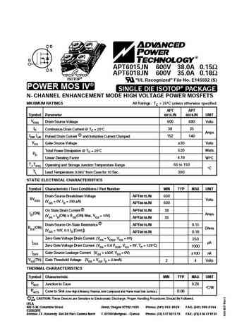
D G APT6015JN 600V 38.0A 0.15 S APT6018JN 600V 35.0A 0.18 ISOTOP "UL Recognized" File No. E145592 (S) POWER MOS IV SINGLE DIE ISOTOP PACKAGE N- CHANNEL ENHANCEMENT MODE HIGH VOLTAGE POWER MOSFETS MAXIMUM RATINGS All Ratings TC = 25 C unless otherwise specified. APT APT Symbol Parameter 6015JN 6018JN UNIT VDSS Drain-Source Voltage 600 600 Volts ID Continuous Drain Cu
8.1. Size:69K apt
apt6017b2ll.pdf 
APT6017B2LL APT6017LLL 600V 35A 0.170W B2LL TM POWER MOS 7 Power MOS 7TM is a new generation of low loss, high voltage, N-Channel T-MAX TO-264 enhancement mode power MOSFETS. Both conduction and switching losses are addressed with Power MOS 7TM by significantly lowering RDS(ON) and Qg. Power MOS 7TM combines lower conduction and switching losses along with exceptionally fast swi
8.2. Size:147K apt
apt6011b2vfrg apt6011lvfrg.pdf 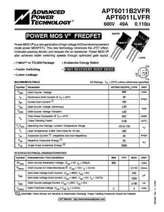
APT6011B2VFR APT6011LVFR 600V 49A 0.110 B2VFR POWER MOS V FREDFET T-MAX TO-264 Power MOS V is a new generation of high voltage N-Channel enhancement mode power MOSFETs. This new technology minimizes the JFET effect, increases packing density and reduces the on-resistance. Power MOS V also achieves faster switching speeds through optimized gate layout.
8.3. Size:70K apt
apt6013b2fll.pdf 
APT6013B2FLL APT6013LFLL 600V 43A 0.130W TM FREDFET POWER MOS 7 B2FLL Power MOS 7TM is a new generation of low loss, high voltage, N-Channel enhancement mode power MOSFETS. Both conduction and switching T-MAX TO-264 losses are addressed with Power MOS 7TM by significantly lowering RDS(ON) and Qg. Power MOS 7TM combines lower conduction and switching losses along with exceptiona
8.4. Size:59K apt
apt6015lvfr.pdf 
APT6015LVFR 600V 38A 0.150W POWER MOS V FREDFET Power MOS V is a new generation of high voltage N-Channel enhancement TO-264 mode power MOSFETs. This new technology minimizes the JFET effect, increases packing density and reduces the on-resistance. Power MOS V also achieves faster switching speeds through optimized gate layout. Fast Recovery Body Diode 100% Avalanche Teste
8.5. Size:60K apt
apt6015b2vr.pdf 
APT6015B2VR 600V 38A 0.150 POWER MOS V T-MAX Power MOS V is a new generation of high voltage N-Channel enhancement mode power MOSFETs. This new technology minimizes the JFET effect, increases packing density and reduces the on-resistance. Power MOS V also achieves faster switching speeds through optimized gate layout. Faster Switching 100% Avalanche Tested D Low
8.6. Size:162K apt
apt6017b2fllg apt6017lfllg.pdf 
APT6017B2FLL APT6017LFLL 600V 35A 0.170 B2FLL R POWER MOS 7 FREDFET T-MAX TO-264 Power MOS 7 is a new generation of low loss, high voltage, N-Channel enhancement mode power MOSFETS. Both conduction and switching losses are addressed with Power MOS 7 by significantly lowering RDS(ON) and Qg. Power MOS 7 combines lower conduction and switching losses L
8.7. Size:37K apt
apt6011lvr.pdf 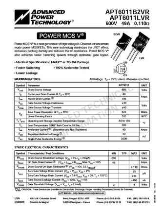
APT6011B2VR APT6011LVR 600V 49A 0.110W B2VR POWER MOS V T-MAX Power MOS V is a new generation of high voltage N-Channel enhancement TO-264 mode power MOSFETs. This new technology minimizes the JFET effect, increases packing density and reduces the on-resistance. Power MOS V also achieves faster switching speeds through optimized gate layout. LVR Identical Specifications
8.8. Size:143K apt
apt6011b2vr.pdf 
APT6011B2VR APT6011LVR 600V 49A 0.110 B2VR POWER MOS V MOSFET T-MAX TO-264 Power MOS V is a new generation of high voltage N-Channel enhancement mode power MOSFETs. This new technology minimizes the JFET effect, increases packing density and reduces the on-resistance. Power MOS V also achieves faster switching speeds through optimized gate layout. LVR
8.9. Size:71K apt
apt6013jvr.pdf 
APT6013JVR 600V 40A 0.130 POWER MOS V Power MOS V is a new generation of high voltage N-Channel enhancement mode power MOSFETs. This new technology minimizes the JFET effect, increases packing density and reduces the on-resistance. Power MOS V also achieves faster switching speeds through optimized gate layout. "UL Recognized" ISOTOP D Faster Switching 100% Avalanch
8.10. Size:69K apt
apt6013b2ll.pdf 
APT6013B2LL APT6013LLL 600V 43A 0.130W B2LL TM POWER MOS 7 Power MOS 7TM is a new generation of low loss, high voltage, N-Channel T-MAX TO-264 enhancement mode power MOSFETS. Both conduction and switching losses are addressed with Power MOS 7TM by significantly lowering RDS(ON) and Qg. Power MOS 7TM combines lower conduction and switching losses along with exceptionally fast swi
8.11. Size:200K apt
apt6013b2llg apt6013lllg.pdf 
APT6013B2LL APT6013LLL 600V 43A 0.130 B2LL R POWER MOS 7 MOSFET T-MAX TO-264 Power MOS 7 is a new generation of low loss, high voltage, N-Channel enhancement mode power MOSFETS. Both conduction and switching losses are addressed with Power MOS 7 by significantly lowering RDS(ON) and Qg. Power MOS 7 combines lower conduction and switching losses LLL
8.12. Size:70K apt
apt6015jvr.pdf 
APT6015JVR 600V 35A 0.150 POWER MOS V Power MOS V is a new generation of high voltage N-Channel enhancement mode power MOSFETs. This new technology minimizes the JFET effect, increases packing density and reduces the on-resistance. Power MOS V also achieves faster switching speeds through optimized gate layout. "UL Recognized" ISOTOP Faster Switching 100% Avalanche T
8.13. Size:60K apt
apt6017wvr.pdf 
APT6017WVR 600V 31.5A 0.170 POWER MOS V TO-267 Power MOS V is a new generation of high voltage N-Channel enhancement mode power MOSFETs. This new technology minimizes the JFET effect, increases packing density and reduces the on-resistance. Power MOS V also achieves faster switching speeds through optimized gate layout. Faster Switching 100% Avalanche Tested D Lowe
8.14. Size:62K apt
apt6015lvr.pdf 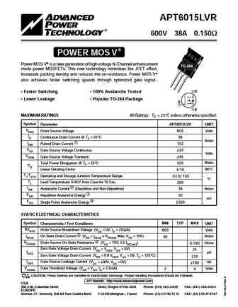
APT6015LVR 600V 38A 0.150 POWER MOS V Power MOS V is a new generation of high voltage N-Channel enhancement TO-264 mode power MOSFETs. This new technology minimizes the JFET effect, increases packing density and reduces the on-resistance. Power MOS V also achieves faster switching speeds through optimized gate layout.. D Faster Switching 100% Avalanche Tested Lowe
8.15. Size:70K apt
apt6013jfll.pdf 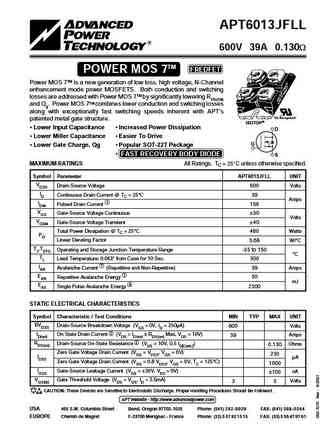
APT6013JFLL 600V 39A 0.130W TM FREDFET POWER MOS 7 Power MOS 7TM is a new generation of low loss, high voltage, N-Channel enhancement mode power MOSFETS. Both conduction and switching losses are addressed with Power MOS 7TM by significantly lowering RDS(ON) and Qg. Power MOS 7TM combines lower conduction and switching losses along with exceptionally fast switching speeds inherent with
8.16. Size:69K apt
apt6010b2ll.pdf 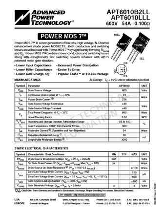
APT6010B2LL APT6010LLL 600V 54A 0.100W B2LL TM POWER MOS 7 Power MOS 7TM is a new generation of low loss, high voltage, N-Channel T-MAX TO-264 enhancement mode power MOSFETS. Both conduction and switching losses are addressed with Power MOS 7TM by significantly lowering RDS(ON) and Qg. Power MOS 7TM combines lower conduction and switching losses along with exceptionally fast swi
8.17. Size:33K apt
apt6011b2vfr.pdf 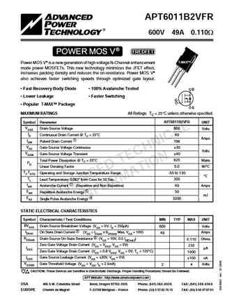
APT6011B2VFR 600V 49A 0.110W POWER MOS V FREDFET T-MAX Power MOS V is a new generation of high voltage N-Channel enhancement mode power MOSFETs. This new technology minimizes the JFET effect, increases packing density and reduces the on-resistance. Power MOS V also achieves faster switching speeds through optimized gate layout. Fast Recovery Body Diode 100% Avalanche Te
8.18. Size:69K apt
apt6013jll.pdf 
APT6013JLL 600V 39A 0.130W TM POWER MOS 7 Power MOS 7TM is a new generation of low loss, high voltage, N-Channel enhancement mode power MOSFETS. Both conduction and switching losses are addressed with Power MOS 7TM by significantly lowering RDS(ON) and Qg. Power MOS 7TM combines lower conduction and switching losses along with exceptionally fast switching speeds inherent with APT's "U
8.19. Size:161K apt
apt6017b2llg apt6017lllg.pdf 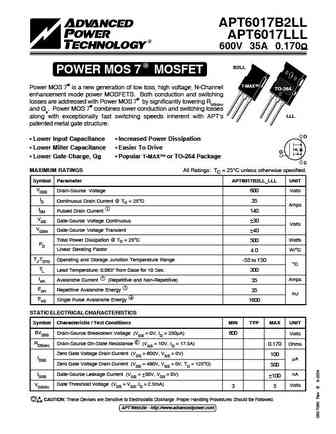
APT6017B2LL APT6017LLL 600V 35A 0.170 R B2LL POWER MOS 7 MOSFET T-MAX Power MOS 7 is a new generation of low loss, high voltage, N-Channel TO-264 enhancement mode power MOSFETS. Both conduction and switching losses are addressed with Power MOS 7 by significantly lowering RDS(ON) and Qg. Power MOS 7 combines lower conduction and switching losses along
8.20. Size:70K apt
apt6010jfll.pdf 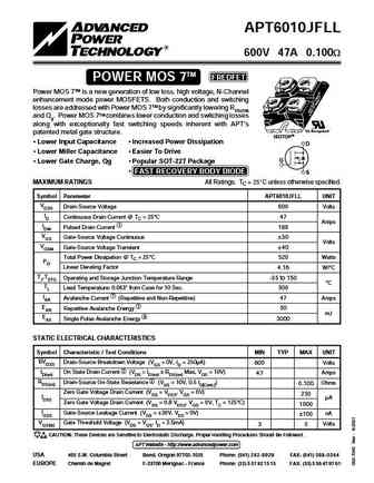
APT6010JFLL 600V 47A 0.100W TM FREDFET POWER MOS 7 Power MOS 7TM is a new generation of low loss, high voltage, N-Channel enhancement mode power MOSFETS. Both conduction and switching losses are addressed with Power MOS 7TM by significantly lowering RDS(ON) and Qg. Power MOS 7TM combines lower conduction and switching losses along with exceptionally fast switching speeds inherent with
8.21. Size:62K apt
apt6015jn.pdf 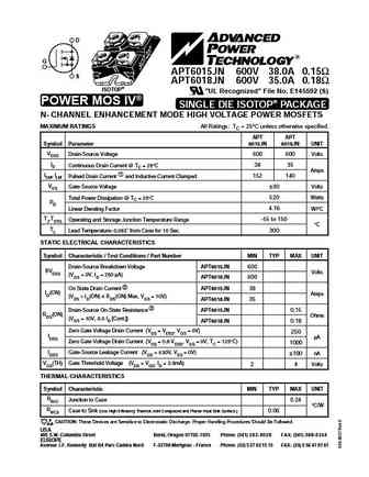
D G APT6015JN 600V 38.0A 0.15 S APT6018JN 600V 35.0A 0.18 ISOTOP "UL Recognized" File No. E145592 (S) POWER MOS IV SINGLE DIE ISOTOP PACKAGE N- CHANNEL ENHANCEMENT MODE HIGH VOLTAGE POWER MOSFETS MAXIMUM RATINGS All Ratings TC = 25 C unless otherwise specified. APT APT Symbol Parameter 6015JN 6018JN UNIT VDSS Drain-Source Voltage 600 600 Volts ID Continuous Drain Cu
8.22. Size:142K apt
apt6013b2fllg apt6013lfllg.pdf 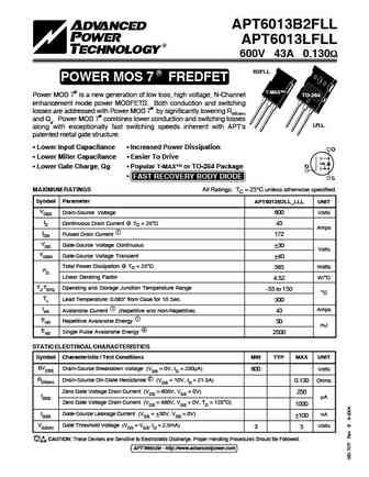
APT6013B2FLL APT6013LFLL 600V 43A 0.130 B2FLL R POWER MOS 7 FREDFET T-MAX TO-264 Power MOS 7 is a new generation of low loss, high voltage, N-Channel enhancement mode power MOSFETS. Both conduction and switching losses are addressed with Power MOS 7 by significantly lowering RDS(ON) and Qg. Power MOS 7 combines lower conduction and switching losses L
8.23. Size:60K apt
apt6015.pdf 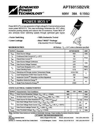
APT6015B2VR 600V 38A 0.150 POWER MOS V T-MAX Power MOS V is a new generation of high voltage N-Channel enhancement mode power MOSFETs. This new technology minimizes the JFET effect, increases packing density and reduces the on-resistance. Power MOS V also achieves faster switching speeds through optimized gate layout. Faster Switching 100% Avalanche Tested D Low
8.24. Size:33K apt
apt6011lvfr.pdf 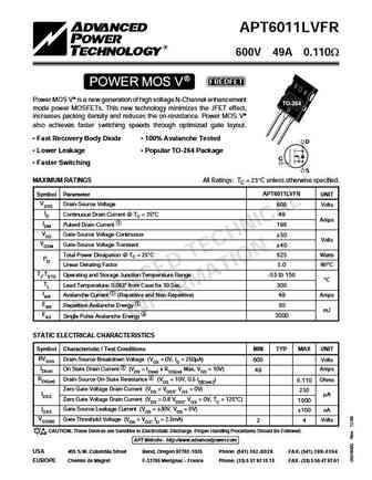
APT6011LVFR 600V 49A 0.110W POWER MOS V FREDFET Power MOS V is a new generation of high voltage N-Channel enhancement TO-264 mode power MOSFETs. This new technology minimizes the JFET effect, increases packing density and reduces the on-resistance. Power MOS V also achieves faster switching speeds through optimized gate layout. Fast Recovery Body Diode 100% Avalanche Teste
8.25. Size:69K apt
apt6010jll.pdf 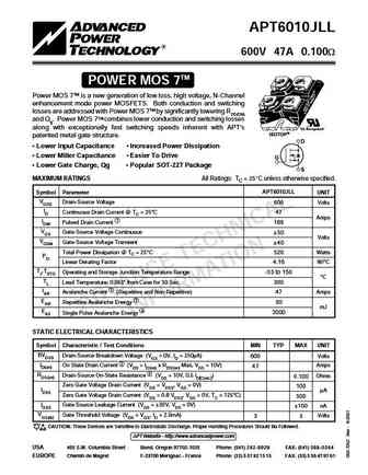
APT6010JLL 600V 47A 0.100W TM POWER MOS 7 Power MOS 7TM is a new generation of low loss, high voltage, N-Channel enhancement mode power MOSFETS. Both conduction and switching losses are addressed with Power MOS 7TM by significantly lowering RDS(ON) and Qg. Power MOS 7TM combines lower conduction and switching losses along with exceptionally fast switching speeds inherent with APT's "U
8.26. Size:113K apt
apt6015b2vfrg apt6015lvfrg.pdf 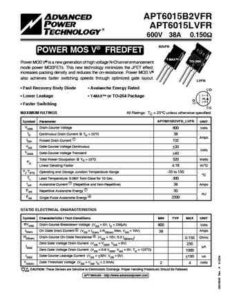
APT6015B2VFR APT6015LVFR 600V 38A 0.150 B2VFR POWER MOS V FREDFET T-MAX TO-264 Power MOS V is a new generation of high voltage N-Channel enhancement mode power MOSFETs. This new technology minimizes the JFET effect, increases packing density and reduces the on-resistance. Power MOS V also achieves faster switching speeds through optimized gate layout.
8.27. Size:70K apt
apt6017jfll.pdf 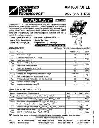
APT6017JFLL 600V 31A 0.170W TM FREDFET POWER MOS 7 Power MOS 7TM is a new generation of low loss, high voltage, N-Channel enhancement mode power MOSFETS. Both conduction and switching losses are addressed with Power MOS 7TM by significantly lowering RDS(ON) and Qg. Power MOS 7TM combines lower conduction and switching losses along with exceptionally fast switching speeds inherent with
8.28. Size:70K apt
apt6017b2fll.pdf 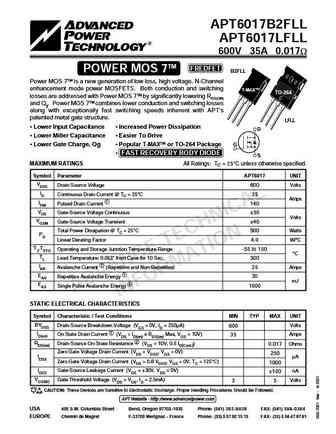
APT6017B2FLL APT6017LFLL 600V 35A 0.017W TM FREDFET POWER MOS 7 B2FLL Power MOS 7TM is a new generation of low loss, high voltage, N-Channel enhancement mode power MOSFETS. Both conduction and switching T-MAX TO-264 losses are addressed with Power MOS 7TM by significantly lowering RDS(ON) and Qg. Power MOS 7TM combines lower conduction and switching losses along with exceptiona
8.29. Size:69K apt
apt6017jll.pdf 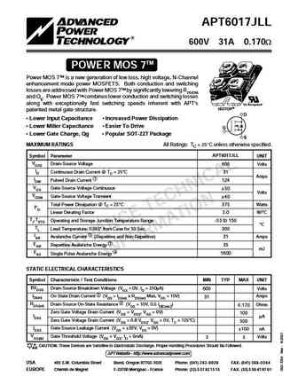
APT6017JLL 600V 31A 0.170W TM POWER MOS 7 Power MOS 7TM is a new generation of low loss, high voltage, N-Channel enhancement mode power MOSFETS. Both conduction and switching losses are addressed with Power MOS 7TM by significantly lowering RDS(ON) and Qg. Power MOS 7TM combines lower conduction and switching losses along with exceptionally fast switching speeds inherent with APT's "U
8.30. Size:136K microsemi
apt6015jvfr.pdf 
APT6015JVFR 600V 35A 0.150W FREDFET POWER MOS V Power MOS V is a new generation of high voltage N-Channel enhance- ment mode power MOSFETs. This new technology minimizes the JFET ef- fect, increases packing density and reduces the on-resistance. Power MOS V also achieves faster switching speeds through optimized gate layout. "UL Recognized" ISOTOP file # E145592 Faster S
8.31. Size:259K microsemi
apt6010b2fllg apt6010lfllg.pdf 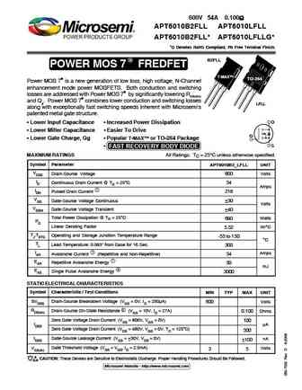
600V 54A 0.100 APT6010B2FLL APT6010LFLL APT6010B2FLL* APT6010LFLLG* *G Denotes RoHS Compliant, Pb Free Terminal Finish. R B2FLL POWER MOS 7 FREDFET T-MAX TO-264 Power MOS 7 is a new generation of low loss, high voltage, N-Channel enhancement mode power MOSFETS. Both conduction and switching losses are addressed with Power MOS 7 by significantly lowering
8.32. Size:258K microsemi
apt6010b2llg apt6010lllg.pdf 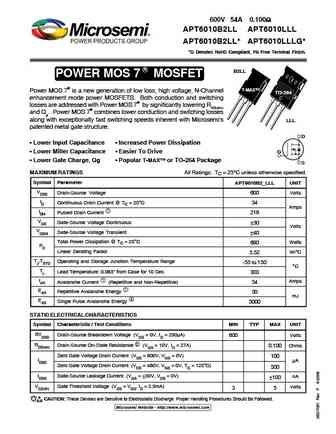
600V 54A 0.100 APT6010B2LL APT6010LLL APT6010B2LL* APT6010LLLG* *G Denotes RoHS Compliant, Pb Free Terminal Finish. R B2LL POWER MOS 7 MOSFET T-MAX Power MOS 7 is a new generation of low loss, high voltage, N-Channel TO-264 enhancement mode power MOSFETS. Both conduction and switching losses are addressed with Power MOS 7 by significantly lowering RDS(O
8.33. Size:376K inchange semiconductor
apt6013b2fll.pdf 
isc N-Channel MOSFET Transistor APT6013B2FLL FEATURES Drain Current I = 43A@ T =25 D C Drain Source Voltage- V =600V(Min) DSS Static Drain-Source On-Resistance R =0.13 (Max) DS(on) 100% avalanche tested Minimum Lot-to-Lot variations for robust device performance and reliable operation DESCRIPTION Designed for use in switch mode power supplies and general pu
8.34. Size:255K inchange semiconductor
apt6015lvfr.pdf 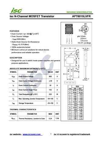
isc N-Channel MOSFET Transistor APT6015LVFR FEATURES Drain Current I = 38A@ T =25 D C Drain Source Voltage- V =600V(Min) DSS Static Drain-Source On-Resistance R =0.15 (Max) DS(on) 100% avalanche tested Minimum Lot-to-Lot variations for robust device performance and reliable operation DESCRIPTION Designed for use in switch mode power supplies and general pur
8.35. Size:255K inchange semiconductor
apt6017lfll.pdf 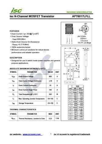
isc N-Channel MOSFET Transistor APT6017LFLL FEATURES Drain Current I = 35A@ T =25 D C Drain Source Voltage- V =600V(Min) DSS Static Drain-Source On-Resistance R =0.17 (Max) DS(on) 100% avalanche tested Minimum Lot-to-Lot variations for robust device performance and reliable operation DESCRIPTION Designed for use in switch mode power supplies and general pur
8.36. Size:376K inchange semiconductor
apt6010b2fll.pdf 
isc N-Channel MOSFET Transistor APT6010B2FLL FEATURES Drain Current I = 54A@ T =25 D C Drain Source Voltage- V =600V(Min) DSS Static Drain-Source On-Resistance R =0.1 (Max) DS(on) 100% avalanche tested Minimum Lot-to-Lot variations for robust device performance and reliable operation DESCRIPTION Designed for use in switch mode power supplies and general pur
8.37. Size:255K inchange semiconductor
apt6010lfll.pdf 
isc N-Channel MOSFET Transistor APT6010LFLL FEATURES Drain Current I = 54A@ T =25 D C Drain Source Voltage- V =600V(Min) DSS Static Drain-Source On-Resistance R =0.1 (Max) DS(on) 100% avalanche tested Minimum Lot-to-Lot variations for robust device performance and reliable operation DESCRIPTION Designed for use in switch mode power supplies and general purp
8.38. Size:376K inchange semiconductor
apt6013b2ll.pdf 
isc N-Channel MOSFET Transistor APT6013B2LL FEATURES Drain Current I = 43A@ T =25 D C Drain Source Voltage- V =600V(Min) DSS Static Drain-Source On-Resistance R =0.13 (Max) DS(on) 100% avalanche tested Minimum Lot-to-Lot variations for robust device performance and reliable operation DESCRIPTION Designed for use in switch mode power supplies and general pur
8.39. Size:376K inchange semiconductor
apt6015b2vfr.pdf 
isc N-Channel MOSFET Transistor APT6015B2VFR FEATURES Drain Current I = 38A@ T =25 D C Drain Source Voltage- V =600V(Min) DSS Static Drain-Source On-Resistance R =0.15 (Max) DS(on) 100% avalanche tested Minimum Lot-to-Lot variations for robust device performance and reliable operation DESCRIPTION Designed for use in switch mode power supplies and general pu
8.40. Size:376K inchange semiconductor
apt6010b2ll.pdf 
isc N-Channel MOSFET Transistor APT6010B2LL FEATURES Drain Current I = 54A@ T =25 D C Drain Source Voltage- V =600V(Min) DSS Static Drain-Source On-Resistance R =0.1 (Max) DS(on) 100% avalanche tested Minimum Lot-to-Lot variations for robust device performance and reliable operation DESCRIPTION Designed for use in switch mode power supplies and general purp
8.41. Size:255K inchange semiconductor
apt6013lfll.pdf 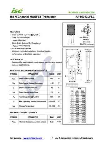
isc N-Channel MOSFET Transistor APT6013LFLL FEATURES Drain Current I = 43A@ T =25 D C Drain Source Voltage- V =600V(Min) DSS Static Drain-Source On-Resistance R =0.13 (Max) DS(on) 100% avalanche tested Minimum Lot-to-Lot variations for robust device performance and reliable operation DESCRIPTION Designed for use in switch mode power supplies and general pur
8.42. Size:376K inchange semiconductor
apt6017b2fll.pdf 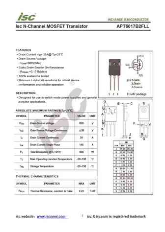
isc N-Channel MOSFET Transistor APT6017B2FLL FEATURES Drain Current I = 35A@ T =25 D C Drain Source Voltage- V =600V(Min) DSS Static Drain-Source On-Resistance R =0.17 (Max) DS(on) 100% avalanche tested Minimum Lot-to-Lot variations for robust device performance and reliable operation DESCRIPTION Designed for use in switch mode power supplies and general pu
Другие IGBT... APT6013LLLG, APT6015B2VFRG, APT6015JVFR, APT6015LVFRG, APT6017B2FLLG, APT6017B2LLG, APT6017LFLLG, APT6017LLLG, NCEP15T14, APT6021BFLLG, APT6021BLLG, APT6021SFLLG, APT6025BFLLG, APT6025BLLG, APT6025BVFRG, APT6025BVRG, APT6025SFLLG
