NTTFS4932NTAG. Аналоги и основные параметры
Наименование производителя: NTTFS4932NTAG
Тип транзистора: MOSFET
Полярность: N
Предельные значения
Pd ⓘ - Максимальная рассеиваемая мощность: 0.85 W
|Vds|ⓘ - Максимально допустимое напряжение сток-исток: 30 V
|Vgs|ⓘ - Максимально допустимое напряжение затвор-исток: 20 V
|Id| ⓘ - Максимально допустимый постоянный ток стока: 11 A
Tj ⓘ - Максимальная температура канала: 150 °C
Электрические характеристики
tr ⓘ - Время нарастания: 22.6 ns
Cossⓘ - Выходная емкость: 1064 pf
RDSonⓘ - Сопротивление сток-исток открытого транзистора: 0.004 Ohm
Тип корпуса: WDFN8
Аналог (замена) для NTTFS4932NTAG
- подборⓘ MOSFET транзистора по параметрам
NTTFS4932NTAG даташит
nttfs4932ntag.pdf

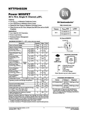
NTTFS4932N Power MOSFET 30 V, 79 A, Single N-Channel, m8FL Features Low RDS(on) to Minimize Conduction Losses Low Capacitance to Minimize Driver Losses http //onsemi.com Optimized Gate Charge to Minimize Switching Losses These Devices are Pb-Free, Halogen Free/BFR Free and are RoHS V(BR)DSS RDS(on) MAX ID MAX Compliant Applications 4.0 mW @ 10 V 30 V 79 A Low-S
nttfs4932n.pdf

NTTFS4932N MOSFET Power, Single, N-Channel, m8FL 30 V, 79 A Features http //onsemi.com Low RDS(on) to Minimize Conduction Losses Low Capacitance to Minimize Driver Losses V(BR)DSS RDS(on) MAX ID MAX Optimized Gate Charge to Minimize Switching Losses These Devices are Pb-Free, Halogen Free/BFR Free and are RoHS 4.0 mW @ 10 V 30 V 79 A Compliant 5.5 mW @ 4.5 V A
nttfs4932n-d.pdf
NTTFS4932N Power MOSFET 30 V, 79 A, Single N-Channel, m8FL Features Low RDS(on) to Minimize Conduction Losses Low Capacitance to Minimize Driver Losses http //onsemi.com Optimized Gate Charge to Minimize Switching Losses These Devices are Pb-Free, Halogen Free/BFR Free and are RoHS V(BR)DSS RDS(on) MAX ID MAX Compliant Applications 4.0 mW @ 10 V 30 V 79 A Low-S
nttfs4930n.pdf

NTTFS4930N Power MOSFET 30 V, 23 A, Single N-Channel, m8FL Features Low RDS(on) to Minimize Conduction Losses Low Capacitance to Minimize Driver Losses http //onsemi.com Optimized Gate Charge to Minimize Switching Losses These Devices are Pb-Free, Halogen Free/BFR Free and are RoHS V(BR)DSS RDS(on) MAX ID MAX Compliant Applications 23 mW @ 10 V 30 V 23 A DC-DC


Другие MOSFET... NTTFS3A08PZ , NTTFS3A08PZTAG , NTTFS4821NTAG , NTTFS4823NTAG , NTTFS4824NTAG , NTTFS4928NTAG , NTTFS4929NTAG , NTTFS4930NTAG , IRFP250 , NTTFS4937NTAG , NTTFS4939NTAG , NTTFS4941NTAG , NTTFS4985NF , NTTFS4C05N , NTTFS4C06N , NTTFS4C08N , NTTFS4C10N .
History: IPA045N10N3
History: IPA045N10N3
🌐 : EN ES РУ

Список транзисторов
Обновления
MOSFET: AUB034N10 | AUB033N08BG | AUB026N085 | AUA062N08BG | AUA060N08AG | AUA056N08BGL | AUA039N10 | ASW80R290E | ASW65R120EFD | ASW65R110E | ASW65R095EFD | ASW65R046EFD | ASW65R041EFDA | ASW65R041E | ASW60R150E | ASW60R090EFDA
Popular searches
c3198 transistor | irfb3607pbf datasheet | 60n60 | 2n5485 equivalent | 2sa1941 | 2sc485 | 2sd287 | 2sd438