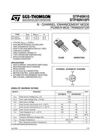
40N10. Аналоги и основные параметры
Наименование производителя: 40N10
Тип транзистора: MOSFET
Полярность: N
Предельные значения
Pd ⓘ - Максимальная рассеиваемая мощность: 150 W
|Vds|ⓘ - Максимально допустимое напряжение сток-исток: 100 V
|Vgs|ⓘ - Максимально допустимое напряжение затвор-исток: 30 V
|Id| ⓘ - Максимально допустимый постоянный ток стока: 40 A
Tj ⓘ - Максимальная температура канала: 150 °C
Электрические характеристики
tr ⓘ - Время нарастания: 30 ns
Cossⓘ - Выходная емкость: 2500 pf
RDSonⓘ - Сопротивление сток-исток открытого транзистора: 0.04 Ohm
Тип корпуса: TO-220C
Аналог (замена) для 40N10
- подборⓘ MOSFET транзистора по параметрам
40N10 даташит
40n10.pdf
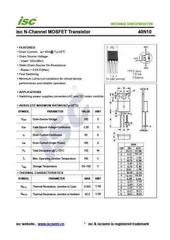
INCHANGE Semiconductor isc N-Channel MOSFET Transistor 40N10 FEATURES Drain Current I = 40A@ T =25 D C Drain Source Voltage- V = 100V(Min) DSS Static Drain-Source On-Resistance R = 0.04 (Max) DS(on) Fast Switching Minimum Lot-to-Lot variations for robust device performance and reliable operation APPLICATIONS Switching power supplies,converters,AC and DC mo
mcac40n10ya-tp.pdf
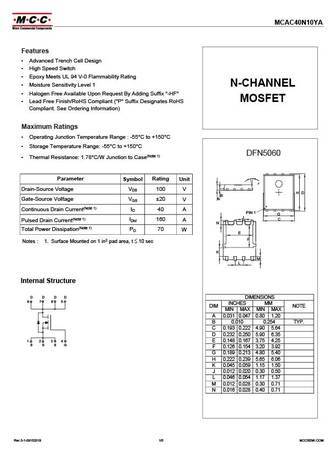
MCAC40N10YA Electrical Characteristics @ 25 C (Unless Otherwise Specified) Parameter Symbol Test Conditions Min Typ Max Unit Static Characteristics V(BR)DSS VGS=0V, ID=250 A Drain-Source Breakdown Voltage 100 V IGSS VDS=0V, VGS = 20V Gate-Source Leakage Current 100 nA IDSS VDS=80V, VGS=0V Zero Gate Voltage Drain Current 1 A 2 4 V Gate-Threshold Voltage(Note 2 VGS(th) VDS


sth240n10f7-2 sth240n10f7-6.pdf
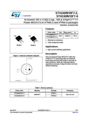
STH240N10F7-2, STH240N10F7-6 N-channel 100 V, 0.002 typ., 180 A STripFET F7 Power MOSFETs in H2PAK-2 and H2PAK-6 packages Datasheet - production data Features Order codes VDS RDS(on)max. ID STH240N10F7-2 TAB TAB 100 V 0.0025 180 A STH240N10F7-6 Ultra low on-resistance 2 7 3 100% avalanche tested 1 1 H2PAK-2 H2PAK-6 Applications High current switchin
stl40n10f7.pdf
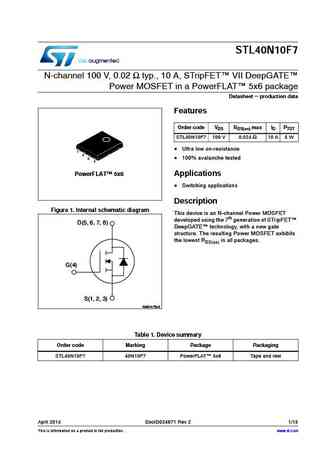
STL40N10F7 N-channel 100 V, 0.02 typ., 10 A, STripFET VII DeepGATE Power MOSFET in a PowerFLAT 5x6 package Datasheet - production data Features Order code VDS RDS(on) max ID PTOT STL40N10F7 100 V 0.024 10 A 5 W Ultra low on-resistance 1 2 3 100% avalanche tested 4 PowerFLAT 5x6 Applications Switching applications Description Figure 1. Internal sche
stp240n10f7.pdf
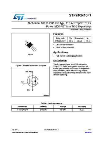
STP240N10F7 N-channel 100 V, 2.85 m typ., 110 A STripFET F7 Power MOSFET in a TO-220 package Datasheet - production data Features Order code VDS RDS(on)max. ID TAB STP240N10F7 100 V 3.2 m 110 A Ultra low on-resistance 100% avalanche tested 3 2 1 Applications TO-220 High current switching applications Description This N-channel Power MOSFET utilizes the F
np40n10pdf np40n10vdf np40n10ydf.pdf
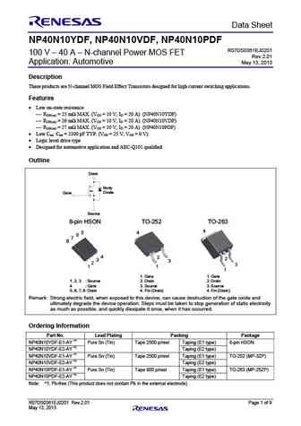
Preliminary Data Sheet NP40N10YDF, NP40N10VDF, NP40N10PDF R07DS0361EJ0201 100 V 40 A N-channel Power MOS FET Rev.2.01 Application Automotive May 13, 2013 Description These products are N-channel MOS Field Effect Transistors designed for high current switching applications. Features Low on-state resistance RDS(on) = 25 m MAX. (VGS = 10 V, ID = 20 A) (NP40N10Y
rf1s40n10.pdf
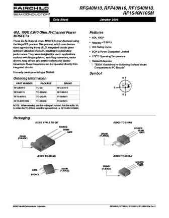
RFG40N10, RFP40N10, RF1S40N10, RF1S40N10SM Data Sheet January 2002 40A, 100V, 0.040 Ohm, N-Channel Power Features MOSFETs 40A, 100V These are N-Channel power MOSFETs manufactured using rDS(ON) = 0.040 the MegaFET process. This process, which uses feature UIS Rating Curve sizes approaching those of LSI integrated circuits gives optimum utilization of silicon, resulti
fqh140n10.pdf
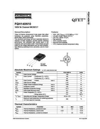
TM QFET FQH140N10 100V N-Channel MOSFET General Description Features These N-Channel enhancement mode power field effect 140A, 100V, RDS(on) = 0.01 @VGS = 10 V transistors are produced using Fairchild s proprietary, Low gate charge ( typical 220 nC) planar stripe, DMOS technology. Low Crss ( typical 470 pF) This advanced technology has been especially tailored to
fqa140n10.pdf
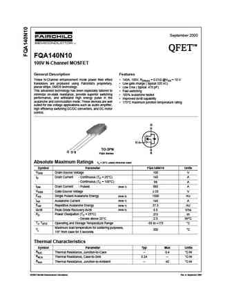
September 2000 TM QFET QFET QFET QFET FQA140N10 100V N-Channel MOSFET General Description Features These N-Channel enhancement mode power field effect 140A, 100V, RDS(on) = 0.01 @VGS = 10 V transistors are produced using Fairchild s proprietary, Low gate charge ( typical 220 nC) planar stripe, DMOS technology. Low Crss ( typical 470 pF) This advanced technology has
rfg40n10 rfp40n10 rf1s40n10-sm.pdf

RFG40N10, RFP40N10, RF1S40N10, RF1S40N10SM Data Sheet January 2002 40A, 100V, 0.040 Ohm, N-Channel Power Features MOSFETs 40A, 100V These are N-Channel power MOSFETs manufactured using rDS(ON) = 0.040 the MegaFET process. This process, which uses feature UIS Rating Curve sizes approaching those of LSI integrated circuits gives optimum utilization of silicon, resulti
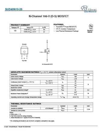
sup40n10-30 sup40n10.pdf
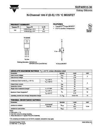
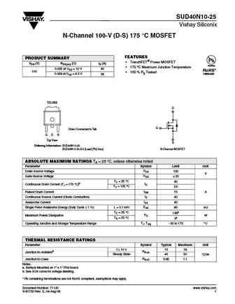
SUP40N10-30 Vishay Siliconix N-Channel 100-V (D-S) 175 C MOSFET FEATURES PRODUCT SUMMARY TrenchFET Power MOSFET V(BR)DSS (V) rDS(on) ( )ID (A) Available 175 C Junction Temperature 0.030 at VGS = 10 V 40 RoHS* 100 0.034 at VGS = 6 V 37.5 COMPLIANT TO-220AB D G G D S Top View S Ordering Information SUP40N10-30 SUP40N10-30-E3 (Lead (Pb)-free) N-Channe
sqr40n10-25.pdf
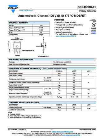
SQR40N10-25 www.vishay.com Vishay Siliconix Automotive N-Channel 100 V (D-S) 175 C MOSFET FEATURES TrenchFET Power MOSFET PRODUCT SUMMARY Package with Low Thermal Resistance VDS (V) 100 100 % Rg and UIS Tested RDS(on) ( ) at VGS = 10 V 0.025 AEC-Q101 Qualified RDS(on) ( ) at VGS = 4.5 V 0.029 Material categorization ID (A) 40 For definitions of com
sud40n10.pdf

SUD40N10-25 Vishay Siliconix N-Channel 100-V (D-S) 175 C MOSFET FEATURES PRODUCT SUMMARY TrenchFET Power MOSFET VDS (V) RDS(on) ( )ID (A) Available 175 C Maximum Junction Temperature 0.025 at VGS = 10 V 40 RoHS* 100 100 % Rg Tested 0.028 at VGS = 4.5 V COMPLIANT 38 TO-252 D G Drain Connected to Tab G D S Top View S Ordering Information SUD40N1
sqd40n10-25.pdf
SQD40N10-25 www.vishay.com Vishay Siliconix Automotive N-Channel 100 V (D-S) 175 C MOSFET FEATURES PRODUCT SUMMARY TrenchFET Power MOSFET VDS (V) 100 Package with Low Thermal Resistance RDS(on) ( ) at VGS = 10 V 0.025 100 % Rg and UIS Tested RDS(on) ( ) at VGS = 4.5 V 0.029 AEC-Q101 Qualified ID (A) 40 Material categorization Configuration Single
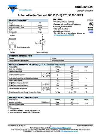
sud40n10-25.pdf
SUD40N10-25 Vishay Siliconix N-Channel 100-V (D-S) 175 C MOSFET FEATURES PRODUCT SUMMARY TrenchFET Power MOSFET VDS (V) RDS(on) ( )ID (A) Available 175 C Maximum Junction Temperature 0.025 at VGS = 10 V 40 RoHS* 100 100 % Rg Tested 0.028 at VGS = 4.5 V COMPLIANT 38 TO-252 D G Drain Connected to Tab G D S Top View S Ordering Information SUD40N1
sum40n10-30.pdf
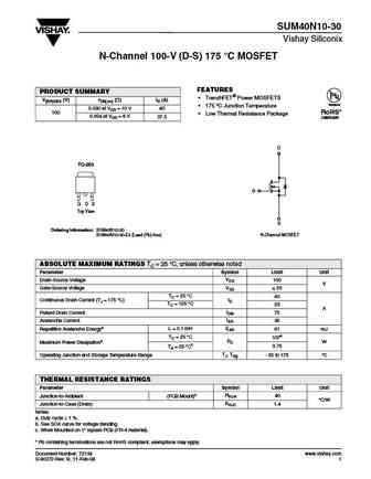
SUM40N10-30 Vishay Siliconix N-Channel 100-V (D-S) 175 C MOSFET FEATURES PRODUCT SUMMARY TrenchFET Power MOSFETS V(BR)DSS (V) rDS(on) ( )ID (A) Available 175 C Junction Temperature 0.030 at VGS = 10 V 40 RoHS* 100 Low Thermal Resistance Package 0.034 at VGS = 6 V 37.5 COMPLIANT D TO-263 G G D S Top View S Ordering Information SUM40N10-30 SUM40N10-
sqm40n10-30.pdf
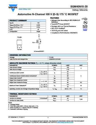
SQM40N10-30 www.vishay.com Vishay Siliconix Automotive N-Channel 100 V (D-S) 175 C MOSFET FEATURES Halogen-free According to IEC 61249-2-21 PRODUCT SUMMARY Definition VDS (V) 100 TrenchFET Power MOSFET RDS(on) ( ) at VGS = 10 V 0.030 Package with Low Thermal Resistance RDS(on) ( ) at VGS = 6 V 0.034 AEC-Q101 Qualifiedd ID (A) 40 100 % Rg and UIS Tested
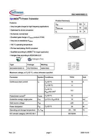
bsz440n10ns3.pdf
BSZ440N10NS3 G Product Summary 3 Power-Transistor V 1 D Features R 44 m D n) m x Q .5BI C I 1 D Q ( @D9=9J54 6?B 43 43 3?>F5BC9?> Q ' 381>>5?B=1
bsc440n10ns3 bsc440n10ns3g.pdf
BSC440N10NS3 G TM 3 Power-Transistor Product Summary Features VDS 100 V %07 *-5 '!2% # (!0'% &-0 ()'( &0%/3%,# 7 !..*)# !2)-,1 RDS(on),max 44 m .2)+ )8%$ &-0 $# $# # -,4%01)-, ID 18 A # (!,,%* ,-0+ !* *%4%* PG-TDSON-8 6# %**%,2 '!2% # (!0'% 6 R product (FOM) DS(on) %07 *-5 -, 0%1)12!,# % R DS(on) 9 -.%0!2),' 2%+ .%0!230% " &0%% *%!$ .*!2),' - # -+ .*)!,2 1)
bsz440n10ns3g.pdf
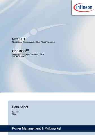
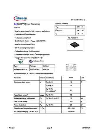
MOSFET Metal Oxide Semiconductor Field Effect Transistor OptiMOSTM OptiMOS 3 Power-Transistor, 100 V BSZ440N10NS3 G Data Sheet Rev. 2.1 Final Power Management & Multimarket OptiMOS 3 Power-Transistor, 100 V BSZ440N10NS3 G S3O8 1 Description 8 7 6 Features 5 Very low gate charge for high frequency applications Optimized for dc-dc conversion N-channel, normal l
bsc040n10ns5sc.pdf
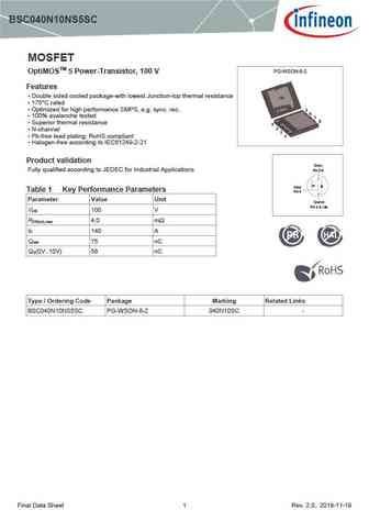
BSC040N10NS5SC MOSFET PG-WSON-8-2 OptiMOSTM 5 Power-Transistor, 100 V Features Double sided cooled package-with lowest Junction-top thermal resistance tab 175 C rated Optimized for high performance SMPS, e.g. sync. rec. 5 6 100% avalanche tested 7 8 Superior thermal resistance 4 3 N-channel 2 1 Pb-free lead plating; RoHS compliant Halogen-fr
bsc040n10ns5.pdf

MOSFET Metal Oxide Semiconductor Field Effect Transistor OptiMOSTM OptiMOSTM 5 Power-Transistor, 100 V BSC040N10NS5 Data Sheet Rev. 2.1 Final Power Management & Multimarket OptiMOSTM 5 Power-Transistor, 100 V BSC040N10NS5 SuperSO8 1 Description 5 8 6 7 Features 7 6 8 5 Optimized for high performance SMPS, e.g. sync. rec. 100% avalanche tested Superior therma
ixtq140n10p ixtt140n10p.pdf
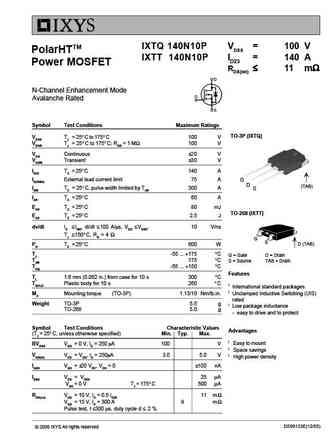
IXTQ 140N10P VDSS = 100 V PolarHTTM IXTT 140N10P ID25 = 140 A Power MOSFET RDS(on) 11 m N-Channel Enhancement Mode Avalanche Rated Symbol Test Conditions Maximum Ratings TO-3P (IXTQ) VDSS TJ = 25 C to 175 C 100 V VDGR TJ = 25 C to 175 C; RGS = 1 M 100 V VGS Continuous 20 V VGSM Transient 30 V ID25 TC = 25 C 140 A ID(RMS)
ixfh140n10p ixft140n10p.pdf
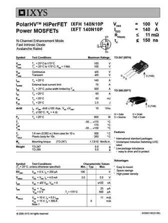
IXFH 140N10P VDSS = 100 V PolarHVTM HiPerFET IXFT 140N10P ID25 = 140 A Power MOSFETs RDS(on) 11 m N-Channel Enhancement Mode trr 150 ns Fast Intrinsic Diode Avalanche Rated Symbol Test Conditions Maximum Ratings TO-247 (IXFH) VDSS TJ = 25 C to 175 C 100 V VDGR TJ = 25 C to 175 C; RGS = 1 M 100 V VGS Continu
mcu40n10.pdf
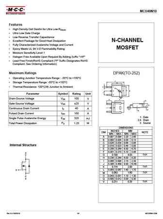
MCU40N10 Features High Density Cell Desihn for Ultra Low RDS(on) Ultra Low Gate Charge Low Reverse Transfer Capacitance Excellent Package for Good Heat Dissipation N-CHANNEL Fully Characterized Avalanche Voltage and Current MOSFET Epoxy Meets UL 94 V-0 Flammability Rating Moisture Sensitivity Level 1 Halogen Free Available Upon Request By Adding Suffix
mcac40n10ya.pdf
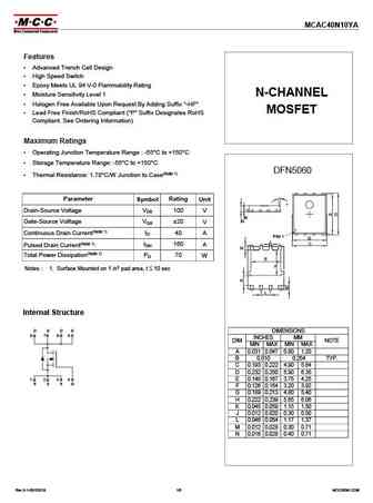
MCAC40N10YA Electrical Characteristics @ 25 C (Unless Otherwise Specified) Parameter Symbol Test Conditions Min Typ Max Unit Static Characteristics V(BR)DSS VGS=0V, ID=250 A Drain-Source Breakdown Voltage 100 V IGSS VDS=0V, VGS = 20V Gate-Source Leakage Current 100 nA IDSS VDS=80V, VGS=0V Zero Gate Voltage Drain Current 1 A 2 4 V Gate-Threshold Voltage(Note 2 VGS(th) VDS
fdbl0240n100.pdf

Is Now Part of To learn more about ON Semiconductor, please visit our website at www.onsemi.com Please note As part of the Fairchild Semiconductor integration, some of the Fairchild orderable part numbers will need to change in order to meet ON Semiconductor s system requirements. Since the ON Semiconductor product management systems do not have the ability to manage part nomenclatur
fqa140n10.pdf

Is Now Part of To learn more about ON Semiconductor, please visit our website at www.onsemi.com Please note As part of the Fairchild Semiconductor integration, some of the Fairchild orderable part numbers will need to change in order to meet ON Semiconductor s system requirements. Since the ON Semiconductor product management systems do not have the ability to manage part nomenclatur
rfg40n10le rfp40n10le rf1s40n10lesm.pdf
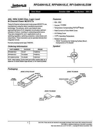
RFG40N10LE, RFP40N10LE, RF1S40N10LESM Data Sheet October 1999 File Number 4061.5 40A, 100V, 0.040 Ohm, Logic Level Features N-Channel Power MOSFETs 40A, 100V These N-Channel enhancement mode power MOSFETs are rDS(ON) = 0.040 manufactured using the latest manufacturing process Temperature Compensating PSPICE Model technology. This process, which uses feature sizes appr
ssd40n10-30d.pdf
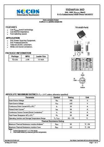
SSD40N10-30D 26A, 100V, RDS(ON) 36m N-Ch Enhancement Mode Power MOSFET Elektronische Bauelemente RoHS Compliant Product A suffix of -C specifies halogen free FEATURES TO-252(D-Pack) Low RDS(on) trench technology. Low thermal impedance. Fast switching speed. APPLICATION PoE Power Sourcing Equipment. A C B PoE Powered Devices. D Telecom DC/DC converte
ceu40n10 ced40n10.pdf
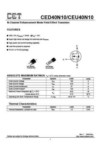
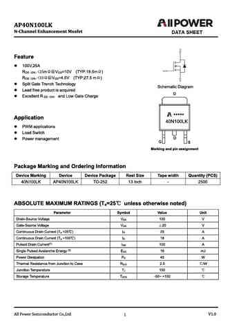
CED40N10/CEU40N10 N-Channel Enhancement Mode Field Effect Transistor FEATURES 100V, 37A, RDS(ON) = 32m @VGS = 10V. Super high dense cell design for extremely low RDS(ON). High power and current handing capability. D Lead free product is acquired. TO-251 & TO-252 package. D G G S CEU SERIES CED SERIES S TO-252(D-PAK) TO-251(I-PAK) ABSOLUTE MAXIMUM RATINGS Tc = 25 C unless oth
cep140n10 ceb140n10.pdf
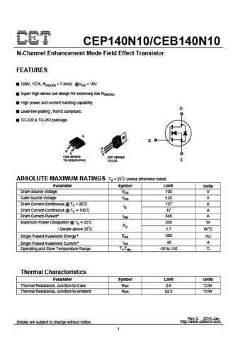
CEP140N10/CEB140N10 N-Channel Enhancement Mode Field Effect Transistor FEATURES 100V, 137A, RDS(ON) = 7.5m @VGS = 10V. Super high dense cell design for extremely low RDS(ON). High power and current handing capability. D Lead-free plating ; RoHS compliant. TO-220 & TO-263 package. G CEB SERIES CEP SERIES TO-263(DD-PAK) S TO-220 ABSOLUTE MAXIMUM RATINGS Tc = 25 C unless otherwise
am40n10-28d.pdf
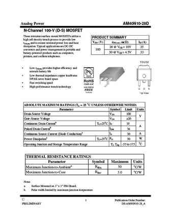
Analog Power AM40N10-28D N-Channel 100-V (D-S) MOSFET These miniature surface mount MOSFETs utilize a PRODUCT SUMMARY high cell density trench process to provide low VDS (V) rDS(on) m( ) ID (A) rDS(on) and to ensure minimal power loss and heat dissipation. Typical applications are DC-DC 28 @ VGS = 10V 35 converters and power management in portable and 100 30 @ VGS = 4.5V 33 bat
am40n10-30d.pdf
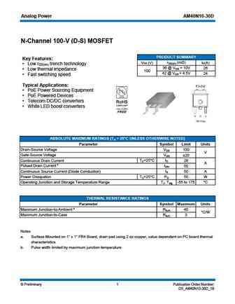
Analog Power AM40N10-30D N-Channel 100-V (D-S) MOSFET PRODUCT SUMMARY Key Features rDS(on) (m ) VDS (V) ID(A) Low r trench technology DS(on) 36 @ VGS = 10V 26 Low thermal impedance 100 42 @ VGS = 4.5V 24 Fast switching speed Typical Applications PoE Power Sourcing Equipment PoE Powered Devices Telecom DC/DC converters White LED boost co
am40n10-30i.pdf
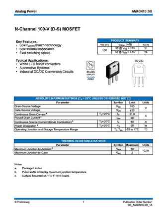
Analog Power AM40N10-30I N-Channel 100-V (D-S) MOSFET PRODUCT SUMMARY Key Features rDS(on) (m ) VDS (V) ID (A) Low r trench technology DS(on) 36 @ VGS = 10V 31 Low thermal impedance 100 42 @ VGS = 4.5V 29 Fast switching speed Typical Applications TO-251 White LED boost converters Automotive Systems Industrial DC/DC Conversion Circuits ABSO
140n10.pdf
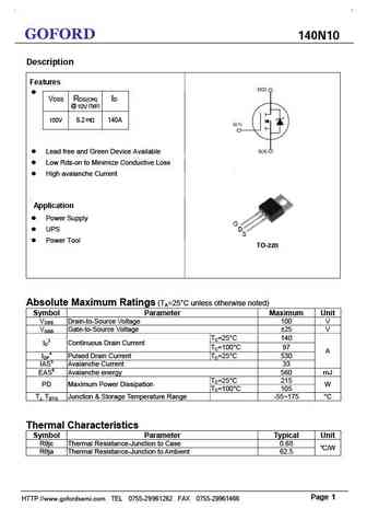
GOFORD 140N10 Description Features VDSS RDS(ON) ID @ 10V (typ) 100V m 6.2 140A Lead free and Green Device Available Low Rds-on to Minimize Conductive Loss High avalanche Current Application Power Supply UPS Power Tool TO-220 Absolute Maximum Ratings (TA=25 C unless otherwise noted) Symbol Parameter Maximum Unit VDSS Drain-to-Source V
40n10k.pdf
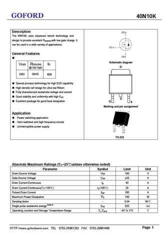
GOFORD 40N10K Description The 40N10K uses advanced trench technology and design to provide excellent RDS(ON) with low gate charge. It can be used in a wide variety of applications. General Features Schematic diagram VDSS RDS(ON) ID @ 10V (typ) m 100V 14 40A Special process technology for high ESD capability High density cell design for ultra low Rdson
crst040n10n crss037n10n.pdf
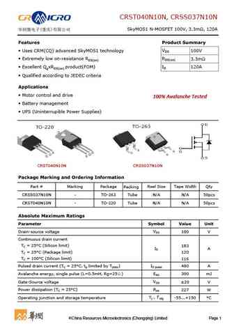
CRST040N10N, CRSS037N10N ( ) SkyMOS1 N-MOSFET 100V, 3.3m , 120A Features Product Summary VDS Uses CRM(CQ) advanced SkyMOS1 technology 100V Extremely low on-resistance RDS(on) RDS(on) 3.3m Excellent QgxRDS(on) product(FOM) ID 120A Qualified according to JEDEC criteria Applications Motor control and drive 100% Avalanche Tested
cs140n10a.pdf
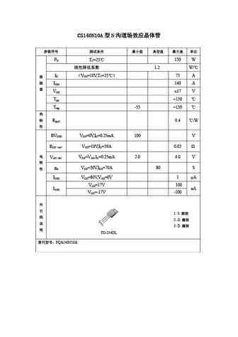
CS140N10A N PD TC=25 150 W 1.2 W/ ID VGS=10V,TC=25 75 A IDM 140 A VGS 17 V Tjm +150 Tstg -55 +150 RthJC 0.4 /W BVDSS VGS=0V,ID=0.25mA 100 V RDS on VGS=10V,ID=39A 0.02 VGS th VDS=VGS,I
ftk40n10d.pdf
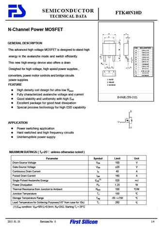
SEMICONDUCTOR FTK40N10D TECHNICAL DATA N-Channel Power MOSFET A I C J GENERAL DESCRIPTION DIM MILLIMETERS This advanced high voltage MOSFET is designed to stand high A 6 50 0 2 B 5 60 0 2 C 5 20 0 2 energy in the avalanche mode and switch efficiently. D 1 50 0 2 E 2 70 0 2 F 2 30 0 1 This new high energy device also offers a drain H H 1 00 MAX I 2 30
dh140n10b dh140n10d.pdf
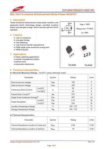
DH140N10B&DH140N10D 68A 100V N-channel Enhancement Mode Power MOSFET 1 Description These N-channel enhancement mode power mosfets used 2 D V = 100V DSS advanced trench technology design, provided excellent Rdson and low gate charge. Which accords with the RoHS G R = 11.0m DS(on) (TYP) standard. 1 3 S I = 68A D 2 Features Low on resistance Low gate charge Fast s
ru140n10r.pdf
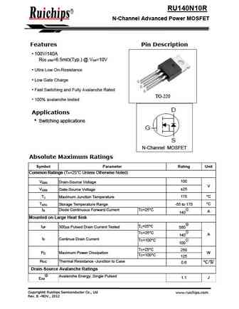
RU140N10R N-Channel Advanced Power MOSFET Features Pin Description 100V/140A RDS (ON)=6.5m (Typ.) @ VGS=10V Ultra Low On-Resistance Low Gate Charge Fast Switching and Fully Avalanche Rated TO-220 100% avalanche tested Applications Switching applications N-Channel MOSFET Absolute Maximum Ratings Symbol Parameter Rating Unit Common Ratings (TA
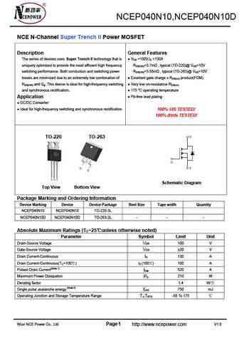
ncep040n10.pdf

NCEP040N10,NCEP040N10D NCE N-Channel Super Trench II Power MOSFET Description General Features The series of devices uses Super Trench II technology that is VDS =100V,ID =130A uniquely optimized to provide the most efficient high frequency RDS(ON)=3.7m , typical (TO-220)@ VGS=10V switching performance. Both conduction and switching power RDS(ON)=3.55m , typical (TO-263)@ VGS=
ncep040n10d.pdf
NCEP040N10,NCEP040N10D NCE N-Channel Super Trench II Power MOSFET Description General Features The series of devices uses Super Trench II technology that is VDS =100V,ID =130A uniquely optimized to provide the most efficient high frequency RDS(ON)=3.7m , typical (TO-220)@ VGS=10V switching performance. Both conduction and switching power RDS(ON)=3.55m , typical (TO-263)@ VGS=
ncep040n10m.pdf
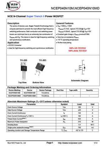
NCEP040N10M,NCEP040N10MD NCE N-Channel Super Trench II Power MOSFET Description General Features The series of devices uses Super Trench II technology that is VDS =100V,ID =130A uniquely optimized to provide the most efficient high frequency RDS(ON)=3.7m , typical (TO-220)@ VGS=10V switching performance. Both conduction and switching power RDS(ON)=3.55m , typical (TO-263)@ VG
ncep040n10gu.pdf
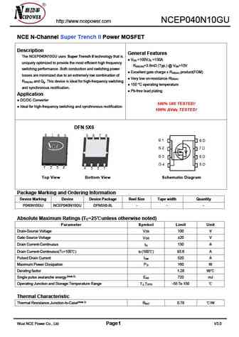
http //www.ncepower.com NCEP040N10GU NCE N-Channel Super Trench II Power MOSFET Description General Features The NCEP040N10GU uses Super Trench II technology that is V =100V,I =130A DS D uniquely optimized to provide the most efficient high frequency R =3.6m (Typ.) @ V =10V DS(ON) GS switching performance. Both conduction and switching power Excellent gate charge x R produc
ncep040n10 ncep040n10d.pdf

NCEP040N10,NCEP040N10D NCE N-Channel Super Trench II Power MOSFET Description General Features The series of devices uses Super Trench II technology that is VDS =100V,ID =130A uniquely optimized to provide the most efficient high frequency RDS(ON)=3.7m , typical (TO-220)@ VGS=10V switching performance. Both conduction and switching power RDS(ON)=3.55m , typical (TO-263)@ VGS=
sw30n06 swp40n10 swi40n10 swd30n06.pdf
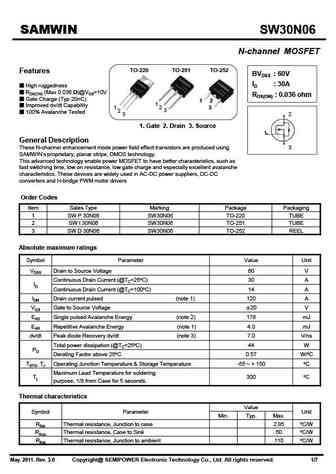
SAMWIN SW30N06 N-channel MOSFET TO-220 TO-251 TO-252 Features BVDSS 60V ID 30A High ruggedness RDS(ON) (Max 0.036 )@VGS=10V RDS(ON) 0.036 ohm Gate Charge (Typ 20nC) 1 2 1 Improved dv/dt Capability 2 1 3 2 3 100% Avalanche Tested 3 2 1. Gate 2. Drain 3. Source 1 General Description These N-channel enhancement mode power field effect transistors
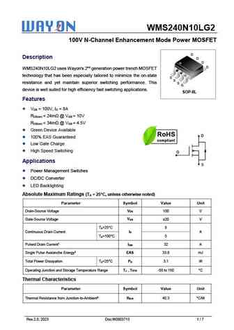
wmo240n10lg2.pdf
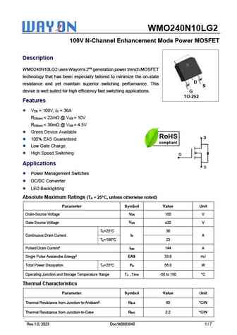
WMO240N10LG2 100V N-Channel Enhancement Mode Power MOSFET Description WMO240N10LG2 uses Wayon's 2nd generation power trench MOSFET technology that has been especially tailored to minimize the on-state D resistance and yet maintain superior switching performance. This S device is well suited for high efficiency fast switching applications. G TO-252 Features V = 100V, I =
fir40n10lg.pdf
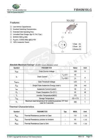
FIR40N10LG 100V N-Channel MOSFET TO-252 Features Low Intrinsic Capacitances. Excellent Switching Characteristics. Extended Safe Operating Area. Unrivalled Gate Charge Qg= 61.7nC (Typ.). BVDSS=100V,ID=40A RDS(on) 0.032 (Max) @VG=10V 100% Avalanche Tested 1.Gate (G) 2.Drain (D) 3.Sourse (S) Absolute Maximum Ratings* (Tc=25 Unless otherwise no
wsf40n10a.pdf
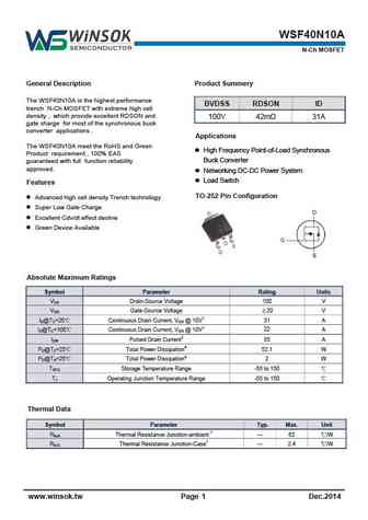
WSF40N10A N-Ch MOSFET General Description Product Summery The WSF40N10A is the highest performance BVDSS RDSON ID trench N-Ch MOSFET with extreme high cell density , which provide excellent RDSON and 100V 42m 31A gate charge for most of the synchronous buck converter applications . Applications The WSF40N10A meet the RoHS and Green High Frequency Point-of-Load Synchron
wsd40n10gdn56.pdf
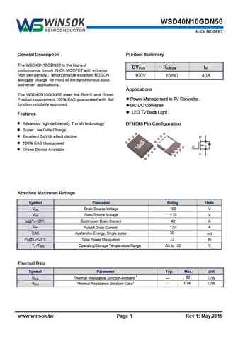
WSD40N10GDN56 N-Ch MOSFET General Description Product Summery The WSD40N10GDN56 is the highest BVDSS RDSON ID performance trench N-Ch MOSFET with extreme high cell density , which provide excellent RDSON 100V 16m 40A and gate charge for most of the synchronous buck converter applications . Applications The WSD40N10GDN56 meet the RoHS and Green Power Management in TV Co
wsf40n10.pdf
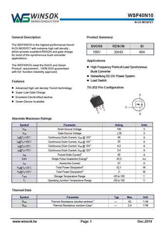
WSF40N10 N-Ch MOSFET General Description Product Summery The WSF40N10 is the highest performance trench BVDSS RDSON ID N-Ch MOSFET with extreme high cell density , which provide excellent RDSON and gate charge 100V 32m 40A for most of the synchronous buck converter applications . Applications The WSF40N10 meet the RoHS and Green High Frequency Point-of-Load Synchronous
rfp40n10.pdf
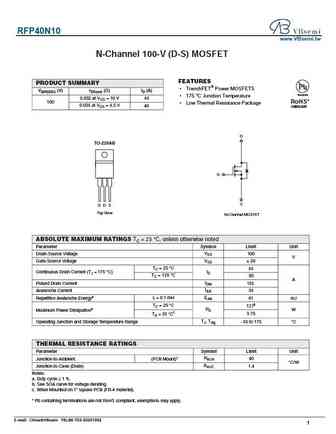
RFP40N10 www.VBsemi.tw N-Channel 100-V (D-S) MOSFET FEATURES PRODUCT SUMMARY TrenchFET Power MOSFETS V(BR)DSS (V) rDS(on) ( )ID (A) Available 175 C Junction Temperature 0.032 at VGS = 10 V 45 RoHS* 100 Low Thermal Resistance Package 0.035 at VGS = 4.5 V 40 COMPLIANT D TO-220AB G S G D S Top View N-Channel MOSFET ABSOLUTE MAXIMUM RATINGS TC = 25 C, un
sud40n10-25.pdf
SUD40N10-25 www.VBsemi.tw N-Channel 100-V (D-S) MOSFET FEATURES PRODUCT SUMMARY TrenchFET Power MOSFETS V(BR)DSS (V) rDS(on) ( )ID (A) Available 175 C Junction Temperature 0.030 at VGS = 10 V 40 RoHS* 100 Low Thermal Resistance Package 0.035 at VGS = 4.5 V 37 COMPLIANT D TO-252 G G D S Top View S N-Channel MOSFET ABSOLUTE MAXIMUM RATINGS TC = 25 C, un
vbze40n10.pdf
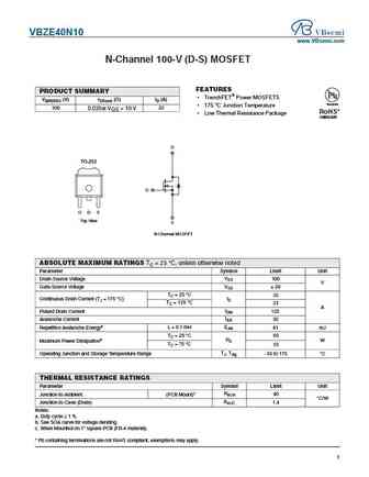
VBZE40N10 www.VBsemi.com N-Channel 100-V (D-S) MOSFET FEATURES PRODUCT SUMMARY TrenchFET Power MOSFETS V(BR)DSS (V) rDS(on) ( )ID (A) Available 175 C Junction Temperature 100 0.035at VGS = 10 V 30 RoHS* Low Thermal Resistance Package COMPLIANT D TO-252 G G D S Top View S N-Channel MOSFET ABSOLUTE MAXIMUM RATINGS TC = 25 C, unless otherwise noted Paramet
vbzm40n10.pdf
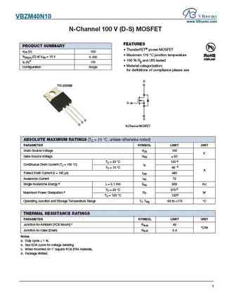
VBZM40N10 www.VBsemi.com N-Channel 100 V (D-S) MOSFET FEATURES PRODUCT SUMMARY ThunderFET power MOSFET VDS (V) 100 Maximum 175 C junction temperature RDS(on) ( ) at VGS = 10 V 0.005 a 100 % Rg and UIS tested ID ( 120 (A) Material categorization Configuration Single for definitions of compliance please see D TO-220AB G S S S D G N-Channel MOSFET
vbzfb40n10.pdf
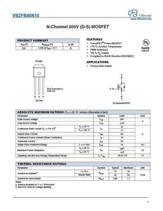
VBZFB40N10 www.VBsemi.com N-Channel 200V (D-S) MOSFET FEATURES PRODUCT SUMMARY TrenchFET Power MOSFET VDS (V) RDS(on) ( )ID (A) 175 C Junction Temperature 0.056 at VGS = 10 V 200 30 PWM Optimized 100 % Rg Tested Compliant to RoHS Directive 2002/95/EC TO-251 APPLICATIONS Primary Side Switch D Drain Connected to G Drain-Tab G D S S Top View N-
tmb140n10a.pdf
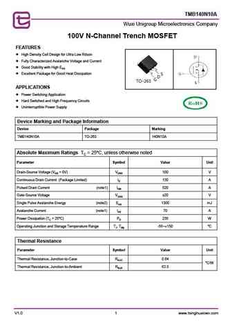
TMB140N10A Wuxi Unigroup Microelectronics Company 100V N-Channel Trench MOSFET FEATURES High Density Cell Design for Ultra Low Rdson Fully Characterized Avalanche Voltage and Current Good Stability with High EAS Excellent Package for Good Heat Dissipation APPLICATIONS Power Switching Application Hard Switched and High Frequency Circuits Uninter
hm40n10k.pdf
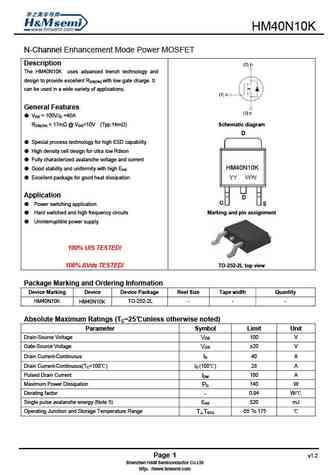
N-Channel Enhancement Mode Power MOSFET Description The uses advanced trench technology and design to provide excellent RDS(ON) with low gate charge. It can be used in a wide variety of applications. General Features VDS = 100V,ID =40A RDS(ON)
hm40n10ka.pdf
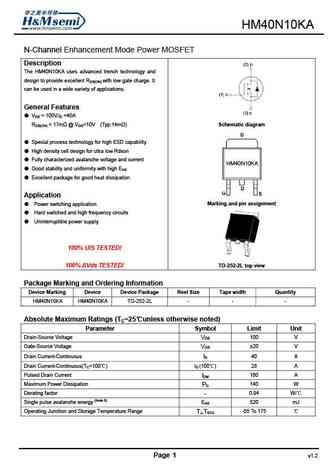
HM40N10KA N-Channel Enhancement Mode Power MOSFET Description The HM40N10KA uses advanced trench technology and design to provide excellent RDS(ON) with low gate charge. It can be used in a wide variety of applications. General Features VDS = 100V,ID =40A RDS(ON)
hms40n10d.pdf
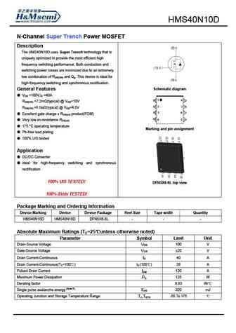
HMS40N10D N-Channel Super Trench Power MOSFET Description The HMS40N10D uses Super Trench technology that is uniquely optimized to provide the most efficient high frequency switching performance. Both conduction and switching power losses are minimized due to an extremely low combination of RDS(ON) and Qg. This device is ideal for high-frequency switching and synchronous rectifi
hm40n10.pdf
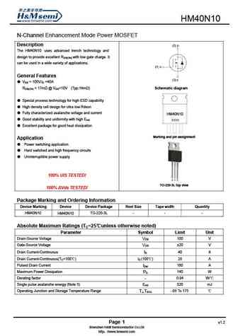
HM40N10 N-Channel Enhancement Mode Power MOSFET Description The HM40N10 uses advanced trench technology and design to provide excellent RDS(ON) with low gate charge. It can be used in a wide variety of applications. General Features VDS = 100V,ID =40A RDS(ON)
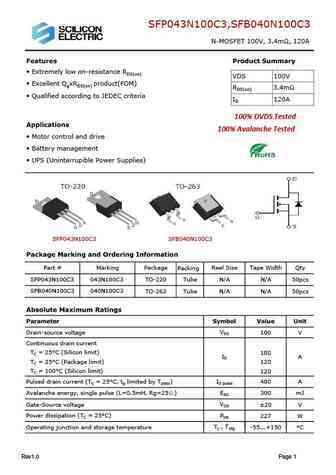
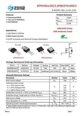
sfp043n100c3 sfb040n100c3.pdf
SFP043N100C3,SFB040N100C3 N-MOSFET 100V, 3.4m , 120A Features Product Summary Extremely low on-resistance RDS(on) VDS 100V Excellent QgxRDS(on) product(FOM) RDS(on) 3.4m Qualified according to JEDEC criteria ID 120A 100% DVDS Tested Applications 100% Avalanche Tested Motor control and drive Battery management UPS (Uninterrupible Power Supplies) SFP
sfp040n100c3 sfb037n100c3.pdf
SFP040N100C3,SFB037N100C3 N-MOSFET 100V, 3.2m , 120A Features Product Summary Enhancement Mode VDS 100V Very Low On-Resistance RDS(on) 3.2m Fast Switching ID 120A 100% DVDS Tested Applications 100% Avalanche Tested Light Electric Vehicles Motor Control and Drive DC/DC Converter,and Genneral Purpose Applications SFP040N100C3 SFB037N100C3 Package Mark
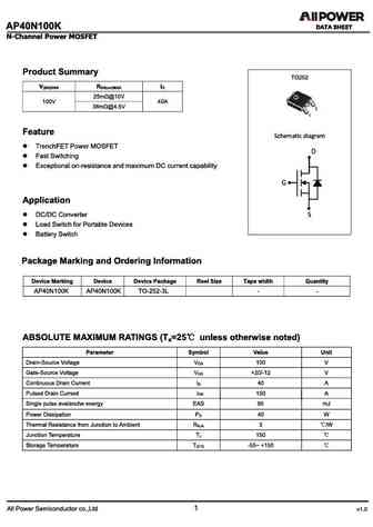
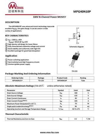
mpg40n10p.pdf
100V N-Channel Power MOSFET DESCRIPTION The MPG40N10P uses advanced trench technology toprovide excellent R , low gate charge. It can be used in a wide DS(ON) variety of applications. KEY CHARACTERISTICS V = 100V,I =40A DS D R
mdt40n10d.pdf
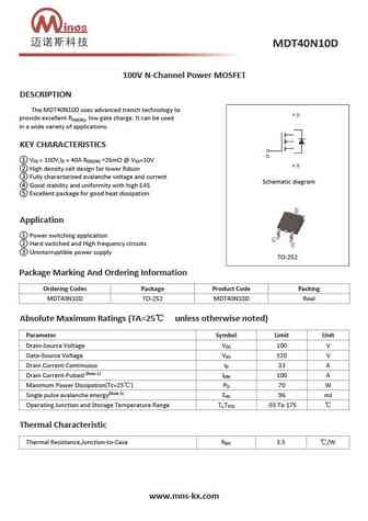
100V N-Channel Power MOSFET DESCRIPTION The MDT40N10D uses advanced trench technology to provide excellent R , low gate charge. It can be used DS(ON) in a wide variety of applications. KEY CHARACTERISTICS V = 100V,I = 40A R
fqa140n10.pdf
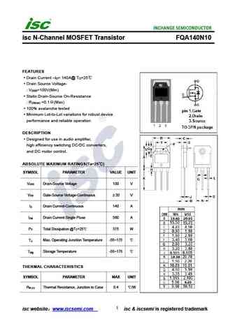
isc N-Channel MOSFET Transistor FQA140N10 FEATURES Drain Current I = 140A@ T =25 D C Drain Source Voltage- V =100V(Min) DSS Static Drain-Source On-Resistance R =0.1 (Max) DS(on) 100% avalanche tested Minimum Lot-to-Lot variations for robust device performance and reliable operation DESCRIPTION Designed for use in audio amplifier, high efficiency switching D
apg40n10df.pdf
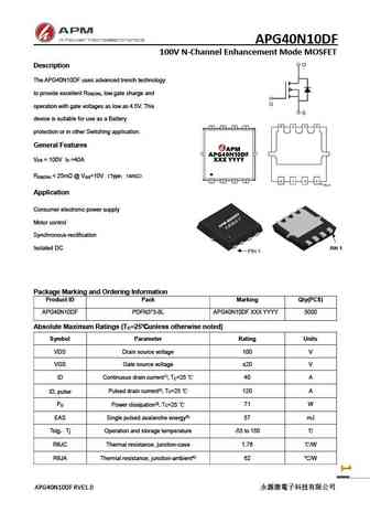
APG40N10DF 100V N-Channel Enhancement Mode MOSFET Description The APG40N10DF uses advanced trench technology to provide excellent R , low gate charge and DS(ON) operation with gate voltages as low as 4.5V. This device is suitable for use as a Battery protection or in other Switching application. General Features V = 100V I =40A DS D R
apg40n10d.pdf
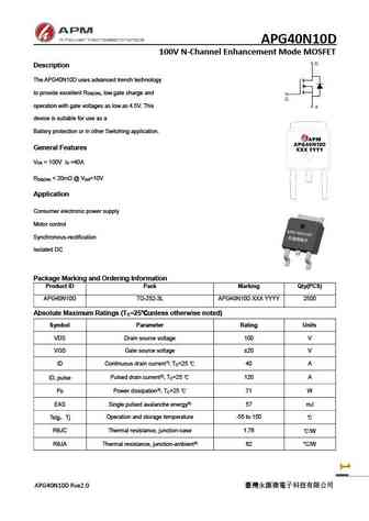
APG40N10D 100V N-Channel Enhancement Mode MOSFET Description The APG40N10D uses advanced trench technology to provide excellent R , low gate charge and DS(ON) operation with gate voltages as low as 4.5V. This device is suitable for use as a Battery protection or in other Switching application. General Features V = 100V I =40A DS D R
apg40n10nf.pdf
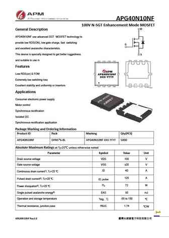
APG40N10NF 100V N-SGT Enhancement Mode MOSFET General Description APG40N10NF use advanced SGT MOSFET technology to provide low RDS(ON), low gate charge, fast switching and excellent avalanche characteristics. This device is specially designed to get better ruggedness and suitable to use in Features Low RDS(on) & FOM Extremely low switching loss Excellent stability and uni
ap40n10p.pdf
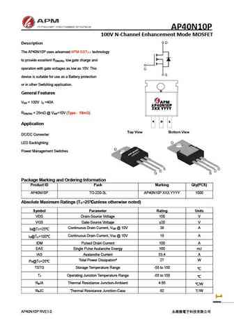
AP40N10P 100V N-Channel Enhancement Mode MOSFET Description The AP40N10P uses advanced APM-SGT technology to provide excellent R , low gate charge and DS(ON) operation with gate voltages as low as 10V. This device is suitable for use as a Battery protection or in other Switching application. General Features V = 100V I =40A DS D R
apg40n10s.pdf
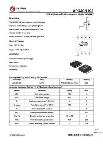
APG40N10S 100V N-Channel Enhancement Mode MOSFET Description The APG40N10D uses advanced trench technology to provide excellent R , low gate charge and DS(ON) operation with gate voltages as low as 4.5V. This device is suitable for use as a Battery protection or in other Switching application. General Features V = 100V I =40A DS D R
Другие MOSFET... 2SK1105 , 2SK1917-M , 2SK1938-01 , 2SK1939-01 , 2SK1982-01M , 2SK2020-01MR , 2SK2645 , 2SK2850 , IRF9540N , 50N15 , 60N05 , 60N05-16 , 60N06-18 , 60N10 , 6N70A , 75N06 , 75N10 .
History: FDMS8050 | FCH190N65F | FCP104N60
History: FDMS8050 | FCH190N65F | FCP104N60
🌐 : EN ES РУ

Список транзисторов
Обновления
MOSFET: ASU70R600E | ASU65R850E | ASU65R550E | ASU65R350E | ASR65R120EFD | ASR65R046EFD | ASQ65R046EFD | ASM65R280E | ASM60R330E | ASE70R950E | ASD80R750E | ASD70R950E | ASD70R600E | ASD70R380E | ASD65R850E | ASD65R550E
Popular searches
irfp450 | mj21193 | s9014 transistor | bc547 transistor datasheet | c945 datasheet | irfp260 | ksc2383 | 2n3773