M7002TTD03. Аналоги и основные параметры
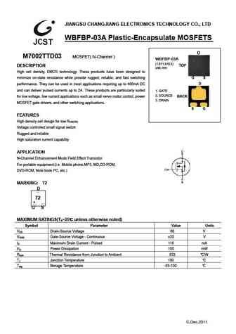
Наименование производителя: M7002TTD03
Тип транзистора: MOSFET
Полярность: N
Предельные значения
Pd ⓘ
- Максимальная рассеиваемая мощность: 0.15 W
|Vds|ⓘ - Максимально допустимое напряжение сток-исток: 60 V
|Vgs|ⓘ - Максимально допустимое напряжение затвор-исток: 20 V
|Id| ⓘ - Максимально допустимый постоянный ток стока: 0.115 A
Tj ⓘ - Максимальная температура канала: 150 °C
Электрические характеристики
Cossⓘ - Выходная емкость: 25 pf
RDSonⓘ - Сопротивление сток-исток открытого транзистора: 7.2 Ohm
Тип корпуса: WBFBP-03A
Аналог (замена) для M7002TTD03
- подборⓘ MOSFET транзистора по параметрам
M7002TTD03 даташит
..1. Size:252K jiangsu
m7002ttd03.pdf 

JIANGSU CHANGJIANG ELECTRONICS TECHNOLOGY CO., LTD WBFBP-03A Plastic-Encapsulate MOSFETS D M7002TTD03 MOSFET( N-Channel ) WBFBP-03A (1.6 1.6 0.5) TOP DESCRIPTION unit mm High cell density, DMOS technology. These products have been designed to G S minimize on-state resistance while provide rugged, reliable, and fast switching D performance. They can be used i
8.1. Size:289K globaltech semi
gsm7002t.pdf 

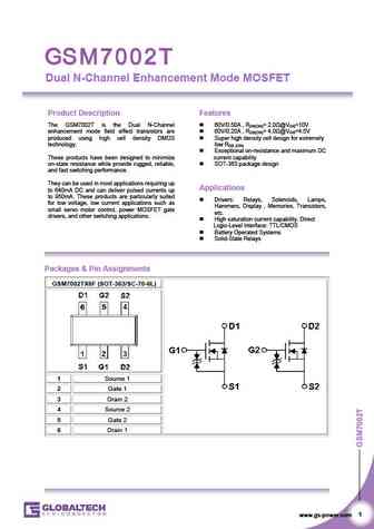
Dual N-Channel Enhancement Mode MOSFET Product Description Features The GSM7002T is the Dual N-Channel 60V/0.50A , RDS(ON)= 2.0 @VGS=10V enhancement mode field effect transistors are 60V/0.20A , RDS(ON)= 4.0 @VGS=4.5V produced using high cell density DMOS Super high density cell design for extremely technology. low RDS (ON) Exceptional on-resistance and maximum
9.1. Size:612K central
ctldm7002a-m621.pdf 

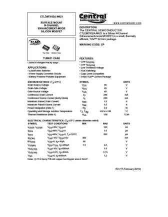
CTLDM7002A-M621 SURFACE MOUNT www.centralsemi.com N-CHANNEL DESCRIPTION ENHANCEMENT-MODE The CENTRAL SEMICONDUCTOR SILICON MOSFET CTLDM7002A-M621 is a Silicon N-Channel Enhancement-mode MOSFET in a small, thermally efficient, TLM 2x1mm package. MARKING CODE CP TLM621 CASE FEATURES Low rDS(ON) Device is Halogen Free by design Low VDS(ON) APPLICATIONS Low
9.2. Size:326K central
cmpdm7002a cmpdm7002a cmpdm7002ag.pdf 

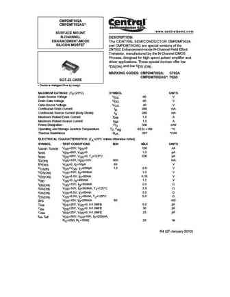
CMPDM7002A CMPDM7002AG* www.centralsemi.com SURFACE MOUNT N-CHANNEL DESCRIPTION ENHANCEMENT-MODE The CENTRAL SEMICONDUCTOR CMPDM7002A SILICON MOSFET and CMPDM7002AG are special versions of the 2N7002 Enhancement-mode N-Channel Field Effect Transistor, manufactured by the N-Channel DMOS Process, designed for high speed pulsed amplifier and driver applications. These special de
9.3. Size:623K central
cmldm7002a cmldm7002a cmldm7002aj.pdf 

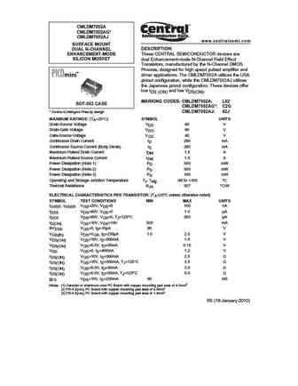
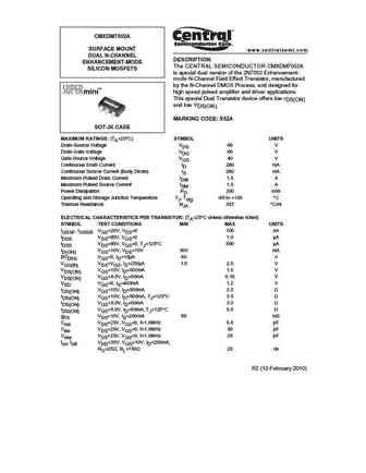
CMLDM7002A CMLDM7002AG* CMLDM7002AJ www.centralsemi.com SURFACE MOUNT DESCRIPTION DUAL N-CHANNEL These CENTRAL SEMICONDUCTOR devices are ENHANCEMENT-MODE SILICON MOSFET dual Enhancement-mode N-Channel Field Effect Transistors, manufactured by the N-Channel DMOS Process, designed for high speed pulsed amplifier and driver applications. The CMLDM7002A utilizes the USA pinout co
9.4. Size:805K central
cedm7002ae.pdf 

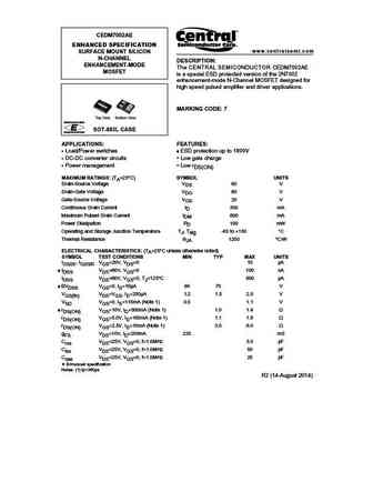
CEDM7002AE ENHANCED SPECIFICATION www.centralsemi.com SURFACE MOUNT SILICON N-CHANNEL DESCRIPTION ENHANCEMENT-MODE The CENTRAL SEMICONDUCTOR CEDM7002AE MOSFET is a special ESD protected version of the 2N7002 enhancement-mode N-Channel MOSFET designed for high speed pulsed amplifier and driver applications. MARKING CODE 7 SOT-883L CASE APPLICATIONS FEATURES Load/Power switc
9.5. Size:785K central
cmpdm7002ae.pdf 

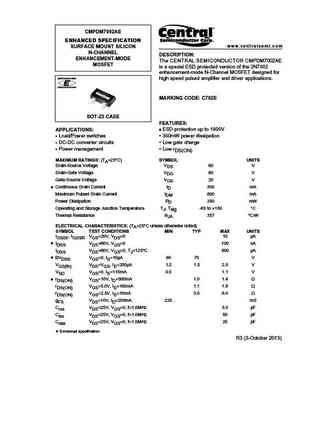
CMPDM7002AE ENHANCED SPECIFICATION www.centralsemi.com SURFACE MOUNT SILICON N-CHANNEL DESCRIPTION ENHANCEMENT-MODE The CENTRAL SEMICONDUCTOR CMPDM7002AE MOSFET is a special ESD protected version of the 2N7002 enhancement-mode N-Channel MOSFET designed for high speed pulsed amplifier and driver applications. MARKING CODE C702E SOT-23 CASE FEATURES ESD protection up to 18
9.6. Size:455K central
ctldm7002a-m621h.pdf 

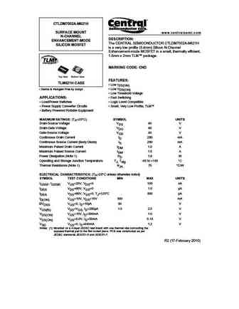
CTLDM7002A-M621H SURFACE MOUNT www.centralsemi.com N-CHANNEL DESCRIPTION ENHANCEMENT-MODE The CENTRAL SEMICONDUCTOR CTLDM7002A-M621H SILICON MOSFET is a very low profile (0.4mm) Silicon N-Channel Enhancement-mode MOSFET in a small, thermally efficient, 1.5mm x 2mm TLM package. MARKING CODE CND FEATURES TLM621H CASE Low rDS(ON) Device is Halogen Free by design
9.7. Size:491K central
cmxdm7002a.pdf 

CMXDM7002A SURFACE MOUNT www.centralsemi.com DUAL N-CHANNEL DESCRIPTION ENHANCEMENT-MODE The CENTRAL SEMICONDUCTOR CMXDM7002A SILICON MOSFETS is special dual version of the 2N7002 Enhancement- mode N-Channel Field Effect Transistor, manufactured by the N-Channel DMOS Process, and designed for high speed pulsed amplifier and driver applications. This special Dual Transistor dev
9.8. Size:379K central
cmpdm7002ahc.pdf 

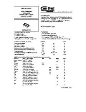
CMPDM7002AHC SURFACE MOUNT www.centralsemi.com N-CHANNEL ENHANCEMENT-MODE DESCRIPTION SILICON MOSFET The CENTRAL SEMICONDUCTOR CMPDM7002AHC is a High Current version of the 2N7002A Enhancement- mode N-Channel MOSFET, designed for high speed pulsed amplifier and driver applications. MARKING CODE 702H SOT-23 CASE Device is Halogen Free by design FEATURES ESD Protectio
9.9. Size:341K jiangsu
m7002nnd03.pdf 

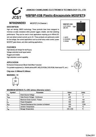
JIANGSU CHANGJIANG ELECTRONICS TECHNOLOGY CO., LTD WBFBP-03B Plastic-Encapsulate MOSFETS D M7002NND03 MOSFET( N-Channel ) WBFBP-03B (1.2 1.2 0.5) TOP DESCRIPTION unit mm High cell density, DMOS technology. These products have been designed to G S minimize on-state resistance while provide rugged, reliable, and fast switching D performance. They can be used i
9.10. Size:188K gsme
gm7002.pdf 

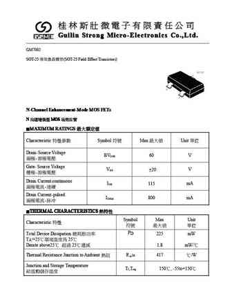
Guilin Strong Micro-Electronics Co.,Ltd. Guilin Strong Micro-Electronics Co.,Ltd. Guilin Strong Micro-Electronics Co.,Ltd. Guilin Strong Micro-Electronics Co.,Ltd. GM7002 SOT-23 (SOT-23 Field Effect Transistors) N-Channel Enhancement-Mode MOS FETs N-Channel Enhancement-Mode MOS FETs N-Channel Enhancement-Mode MOS FET
9.11. Size:814K willsemi
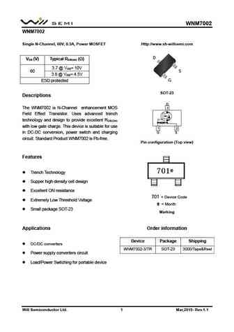
wnm7002.pdf 

WNM7002 WNM7002 Single N-Channel, 60V, 0.3A, Power MOSFET Http //www.sh-willsemi.com D VDS (V) Typical RDS(on) ( ) 3.7 @ VGS= 10V 60 S 3.8 @ VGS= 4.5V G ESD protected SOT-23 Descriptions D The WNM7002 is N-Channel enhancement MOS 3 Field Effect Transistor. Uses advanced trench technology and design to provide excellent RDS(ON) with low gate charge. This device is
9.12. Size:264K sino
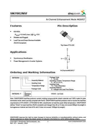
sm7002nsf.pdf 

SM7002NSF N-Channel Enhancement Mode MOSFET Features Pin Description 68V/80A, RDS(ON)=10.8m (max.) @ VGS=10V Reliable and Rugged S D Lead Free and Green Devices Available G (RoHS Compliant) Top View of TO-220 D Applications Synchronous Rectification. G Power Management in Inverter Systems. S N-Channel MOSFET Ordering and Marking Information Package Code SM7002NS
9.13. Size:227K sino
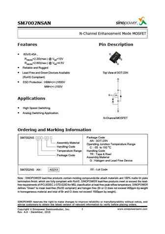
sm7002nsan.pdf 

SM7002NSAN N-Channel Enhancement Mode MOSFET Features Pin Description D 60V/0.45A , RDS(ON)=2.2 (max.) @ VGS=10V S RDS(ON)=2.6 (max.) @ VGS=4.5V G Reliable and Rugged Lead Free and Green Devices Available Top View of SOT-23N (RoHS Compliant) D ESD Protection HBM=(+/-)1600V MM=(+/-)100V G Applications High Speed Switching. S Analog Switching Application. N-Chann
9.14. Size:515K belling
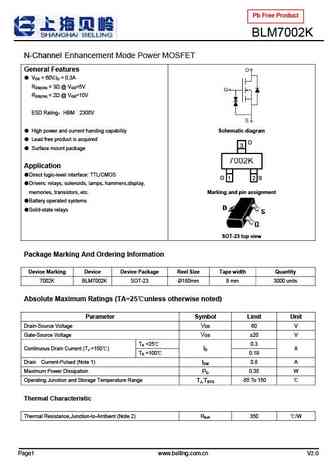
blm7002k.pdf 

Pb Free Product BLM7002K N-Channel Enhancement Mode Power MOSFET General Features VDS = 60V,ID = 0.3A RDS(ON)
9.15. Size:216K belling
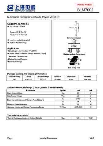
blm7002.pdf 

Pb Free Product BLM7002 N-Channel Enhancement Mode Power MOSFET GENERAL FEATURES V = 60V,I = 0.115A DS D R
9.16. Size:429K globaltech semi
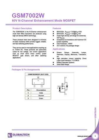
gsm7002w.pdf 

GSM7002W 60V N-Channel Enhancement Mode MOSFET Product Description Features The GSM7002W is the N-Channel enhancement 60V/0.50A , RDS(ON)= 7.5 @VGS=10V mode field effect transistors are produced using 60V/0.05A , RDS(ON)= 7.5 @VGS=5V high cell density DMOS technology. Super high density cell design for extremely low RDS (ON) These products have been designed to minimize
9.17. Size:434K globaltech semi
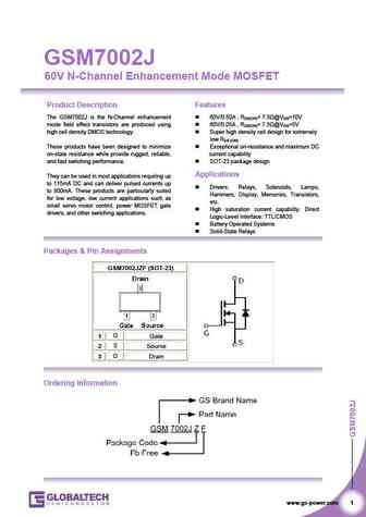
gsm7002j.pdf 

GSM7002J 60V N-Channel Enhancement Mode MOSFET Product Description Features The GSM7002J is the N-Channel enhancement 60V/0.50A , RDS(ON)= 7.5 @VGS=10V mode field effect transistors are produced using 60V/0.05A , RDS(ON)= 7.5 @VGS=5V high cell density DMOS technology. Super high density cell design for extremely low RDS (ON) These products have been designed to minimize
9.18. Size:988K globaltech semi
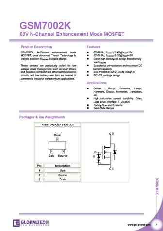
gsm7002k.pdf 

GSM7002K 60V N-Channel Enhancement Mode MOSFET Product Description Features GSM7002K, N-Channel enhancement mode 60V/0.5A , RDS(ON)=2.4 @VGS=10V MOSFET, uses Advanced Trench Technology to 60V/0.3A , RDS(ON)=3.0 @VGS=4.5V provide excellent RDS(ON), low gate charge. Super high density cell design for extremely low RDS (ON) These devices are particularly suited for low E
9.19. Size:808K globaltech semi
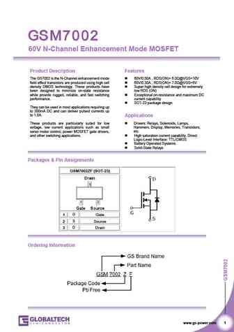
gsm7002.pdf 

60V N-Channel Enhancement Mode MOSFET Product Description Features The GS7002 is the N-Channel enhancement mode 60V/0.50A , RDS(ON)= 6.0 @VGS=10V field effect transistors are produced using high cell 60V/0.30A , RDS(ON)= 7.0 @VGS=5V density DMOS technology. These products have Super high density cell design for extremely been designed to minimize on-state resistance lo
9.20. Size:792K silicon standard
ssm7002egu.pdf 
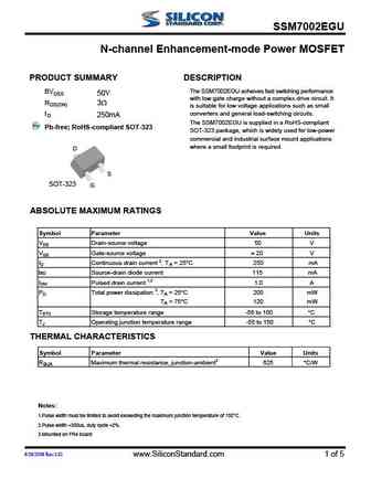
SSM7002EGU N-channel Enhancement-mode Power MOSFET PRODUCT SUMMARY DESCRIPTION The SSM7002EGU acheives fast switching performance BVDSS 50V with low gate charge without a complex drive circuit. It RDS(ON) 3 is suitable for low voltage applications such as small converters and general load-switching circuits. I D 250mA The SSM7002EGU is supplied in a RoHS-compliant Pb-free; RoHS-
9.21. Size:495K silicon standard
ssm7002kgen.pdf 
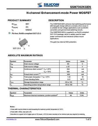
SSM7002KGEN N-channel Enhancement-mode Power MOSFET PRODUCT SUMMARY DESCRIPTION The SSM7002KGEN acheives fast switching performance BVDSS 60V with low gate charge without a complex drive circuit. It RDS(ON) 2 is suitable for low voltage applications such as DC/DC converters and general load-switching circuits. I 640mA D The SSM7002KGEN is supplied in an RoHS-compliant Pb-free; R
9.22. Size:808K silicon standard
ssm7002dgu.pdf 
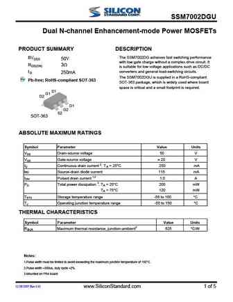
SSM7002DGU Dual N-channel Enhancement-mode Power MOSFETs PRODUCT SUMMARY DESCRIPTION The SSM7002DG acheives fast switching performance BVDSS 50V with low gate charge without a complex drive circuit. It RDS(ON) 3 is suitable for low voltage applications such as DC/DC converters and general load-switching circuits. I D 250mA The SSM7002DGU is supplied in a RoHS-compliant Pb-free;
9.23. Size:826K agertech
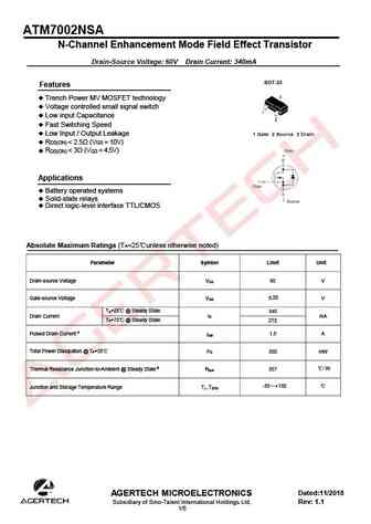
atm7002nsa.pdf 

ATM7002NSA N-Channel Enhancement Mode Field Effect Transistor Drain-Source Voltage 60V Drain Current 340mA Features Trench Power MV MOSFET technology Voltage controlled small signal switch Low input Capacitance Fast Switching Speed Low Input / Output Leakage R
9.24. Size:1840K agertech
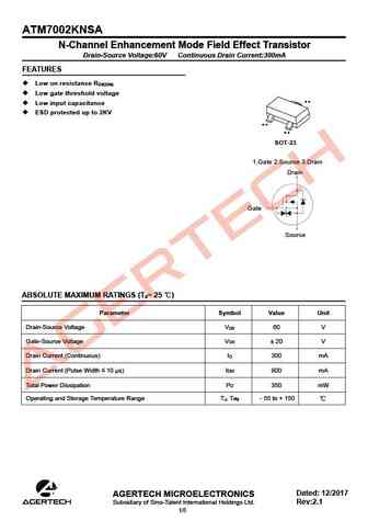
atm7002knsa.pdf 

ATM7002KNSA N-Channel Enhancement Mode Field Effect Transistor Drain-Source Voltage 60V Continuous Drain Current 300mA FEATURES Low on resistance R DS(ON) Low gate threshold voltage Low input capacitance 3 ESD protected up to 2KV 1 2 SOT-23 1.Gate 2.Source 3.Drain Drain Gate Source ABSOLUTE MAXIMUM RATINGS (T = 25 ) a Parameter Symbol Value Unit Drain-Sour
9.25. Size:4097K cn tech public
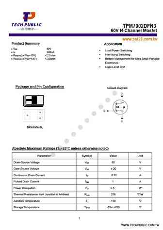
tpm7002dfn3.pdf 

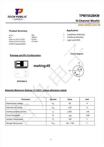
TPM7002DFN3 60V N-Channel Mosfet www.sot23.com.tw Product Summary Application V 60V DS Load/Power Switching I 340mA D Interfacing Switching R ( at V =10V) 2.5ohm DS(ON) GS R ( at V =4.5V) 3.0ohm Battery Management for Ultra Small Portable DS(ON) GS Electronics Logic Level Shift Package and Pin Configuration Circuit diagram D
9.28. Size:691K cn hmsemi
hm7002sr.pdf 

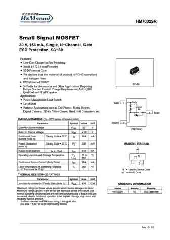
HM7002SR Small Signal MOSFET 30 V, 154 mA, Single, N-Channel, Gate ESD Protection, SC-89 Features Low Gate Charge for Fast Switching Small 1.6 X 1.6 mm Footprint ESD Protected Gate We declare that the material of product is ROHS compliant and halogen free. ESD Protected 2000V ESD Protected 1500V SC-89 S- Prefix for Automotive and Other Applications Requirin
9.29. Size:393K cn hmsemi
hm7002jr.pdf 

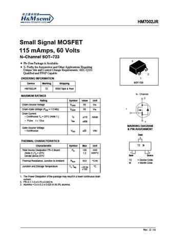
HM7002JR Small Signal MOSFET 115 mAmps, 60 Volts N Channel SOT 723 3 Pb-Free Package is Available. S- Prefix for Automotive and Other Applications Requiring Unique Site and Control Change Requirements; AEC-Q101 Qualified and PPAP Capable. 2 1 ORDERING INFORMATION SOT-723 Device Marking Shipping HM7002JR 72 8000 Tape & Reel N - Channel MAXIMUM RATINGS 3 Rating Sy
9.30. Size:980K cn hmsemi
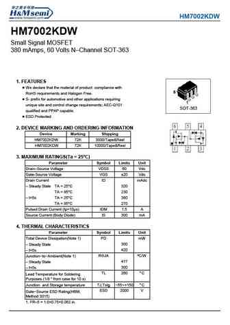
hm7002kdw.pdf 

HM7002KDW HM7002KDW Small Signal MOSFET 380 mAmps, 60 Volts N Channel SOT-363 1. FEATURES We declare that the material of product compliance with RoHS requirements and Halogen Free. S- prefix for automotive and other applications requiring unique site and control change requirements; AEC-Q101 SOT-363 qualified and PPAP capable. ESD Protected 2. DEVICE MARKING AND
9.31. Size:1196K cn hmsemi
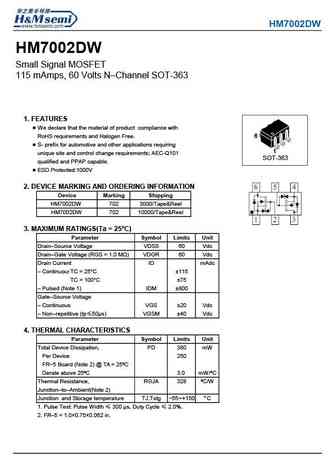
hm7002dw.pdf 

HM7002DW HM7002DW Small Signal MOSFET 115 mAmps, 60 Volts N Channel SOT-363 1. FEATURES We declare that the material of product compliance with RoHS requirements and Halogen Free. S- prefix for automotive and other applications requiring unique site and control change requirements; AEC-Q101 SOT-363 qualified and PPAP capable. ESD Protected 1000V 2. DEVICE MARKIN
9.32. Size:1287K cn hmsemi
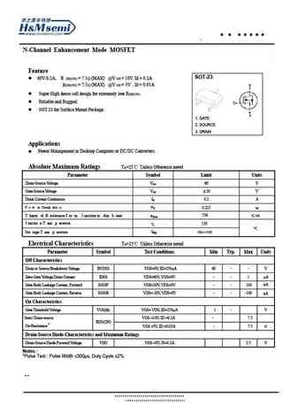
hm7002b.pdf 

HM7002B N-Channel Enhancement Mode MOSFET Feature SOT-23 60V/0.2A, R DS(ON) = 7.5 (MAX) @V GS = 10V. Id = 0. A RDS(ON) = 7.5 (MAX) @V GS = 5V . Id = 0.05A Super High dense cell design for extremely low RDS(ON) . Reliable and Rugged. SOT-23 for Surface Mount Package. 1. GATE 2. SOURCE 3. DRAIN Applications Power Management in Desktop Computer or DC/DC Convert
9.33. Size:380K cn hmsemi
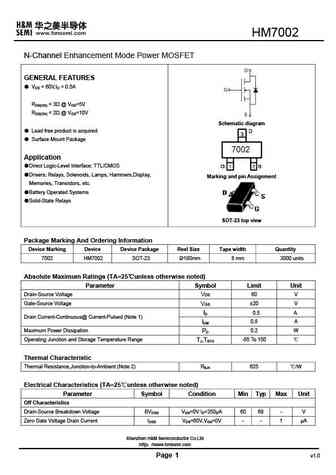
hm7002.pdf 

HM7002 N-Channel Enhancement Mode Power MOSFET GENERAL FEATURES VDS = 60V,ID = 0.5A RDS(ON)
9.34. Size:560K cn hmsemi
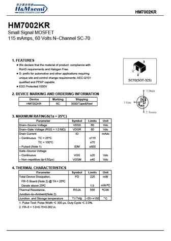
hm7002kr.pdf 

HM7002KR HM7002KR Small Signal MOSFET 115 mAmps, 60 Volts N Channel SC-70 1. FEATURES We declare that the material of product compliance with RoHS requirements and Halogen Free. S- prefix for automotive and other applications requiring unique site and control change requirements; AEC-Q101 SC70(SOT-323) qualified and PPAP capable. ESD Protected 1000V 2. DEVICE MA
9.35. Size:321K cn hmsemi
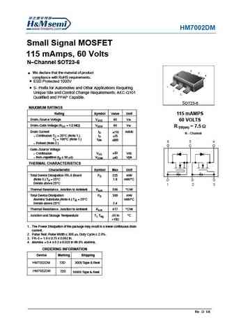
hm7002dm.pdf 

Small Signal MOSFET 115 mAmps, 60 Volts N Channel S We declare that the material of product compliance with RoHS requirements. ESD Protected 1000V S- Prefix for Automotive and Other Applications Requiring Unique Site and Control Change Requirements; AEC-Q101 Qualified and PPAP Capable. S MAXIMUM RATINGS Rating Symbol Value Unit 115 mAMPS
9.36. Size:285K cn haohai electr
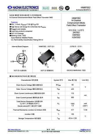
hnm7002.pdf 

HNM7002 N-Channel MOSFETs 115mA,60V N N N-Channel Enhancement Mode Field Effect Transistor SMD HNM7002 N-Channel Features Enhancement Mode 60V, 115mA, RDS(ON)=7.5 @ VGS=5V Field Effect Transistor High dense cell design for extremely low RDS(ON) Rugged
Другие MOSFET... IRFAC32
, JCS24N50WH
, JCS24N50ABH
, RU6888R3
, SPP77N06S2-12
, SPB77N06S2-12
, TSA20N50M
, M7002NND03
, IRFP250N
, MC3406
, MC3541
, MCD04N60
, MCD04N65
, MCD3410
, MS10N60
, MS10N65
, MS10N80
.
History: AOD478
| ELM3C0850A
