4N60CB. Аналоги и основные параметры
Наименование производителя: 4N60CB
Тип транзистора: MOSFET
Полярность: N
Предельные значения
Pd ⓘ
- Максимальная рассеиваемая мощность: 50 W
|Vds|ⓘ - Максимально допустимое напряжение сток-исток: 600 V
|Vgs|ⓘ - Максимально допустимое напряжение затвор-исток: 30 V
|Id| ⓘ - Максимально допустимый постоянный ток стока: 4 A
Tj ⓘ - Максимальная температура канала: 150 °C
Электрические характеристики
tr ⓘ -
Время нарастания: 9 ns
Cossⓘ - Выходная емкость: 54 pf
RDSonⓘ - Сопротивление сток-исток открытого транзистора: 2.2 Ohm
Тип корпуса: TO-220
Аналог (замена) для 4N60CB
- подборⓘ MOSFET транзистора по параметрам
4N60CB даташит
..1. Size:224K 1
4n60cb.pdf 
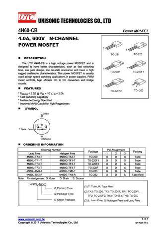
UNISONIC TECHNOLOGIES CO., LTD 4N60-CB Power MOSFET 4.0A, 600V N-CHANNEL POWER MOSFET DESCRIPTION The UTC 4N60-CB is a high voltage power MOSFET and is designed to have better characteristics, such as fast switching time, low gate charge, low on-state resistance and have a high rugged avalanche characteristics. This power MOSFET is usually used at high speed switching appl
0.1. Size:1019K 1
jcs4n60vb jcs4n60rb jcs4n60bb jcs4n60cb jcs4n60fb.pdf 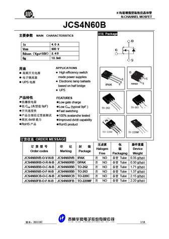
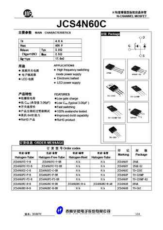
N R N-CHANNEL MOSFET JCS4N60B Package MAIN CHARACTERISTICS 4.0 A ID 600 V VDSS Rdson Vgs=10V 2.4 13.3nC Qg APPLICATIONS High efficiency switch mode power supplies Electronic lamp ballasts UPS based on half bridge UPS
0.2. Size:1045K jilin sino
jcs4n60vb jcs4n60rb jcs4n60bb jcs4n60sb jcs4n60cb jcs4n60fb.pdf 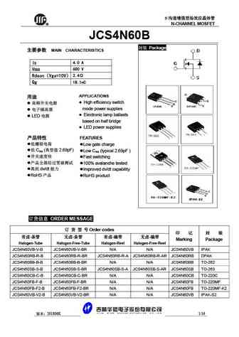
N R N-CHANNEL MOSFET JCS4N60B Package MAIN CHARACTERISTICS ID 4.0 A VDSS 600 V 2.4 Rdson Vgs=10V Qg 18.1nC APPLICATIONS High efficiency switch mode power supplies Electronic lamp ballasts LED based on half bridge LED power su
9.1. Size:801K 1
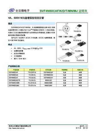
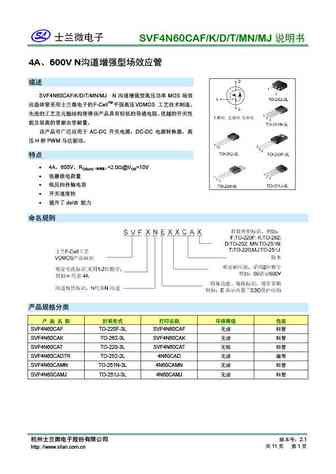
svf4n60caf svf4n60cak svf4n60cad svf4n60cat svf4n60camn svf4n60camj.pdf 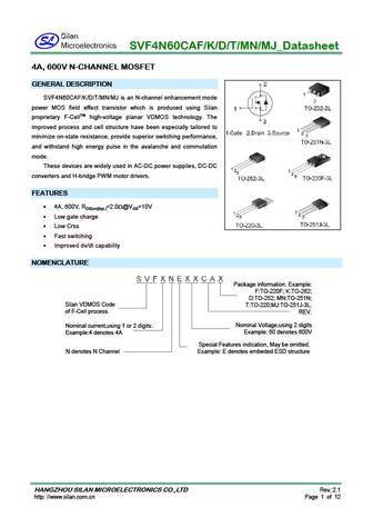
SVF4N60CAF/K/D/T/MN/MJ_Datasheet 4A, 600V N-CHANNEL MOSFET GENERAL DESCRIPTION SVF4N60CAF/K/D/T/MN/MJ is an N-channel enhancement mode power MOS field effect transistor which is produced using Silan proprietary F-CellTM high-voltage planar VDMOS technology. The improved process and cell structure have been especially tailored to minimize on-state resistance, provide superior switc
9.2. Size:345K infineon
spp24n60c3.pdf 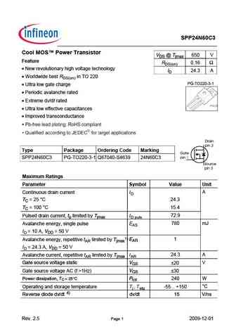
SPP24N60C3 Cool MOS Power Transistor VDS @ Tjmax 650 V Feature RDS(on) 0.16 New revolutionary high voltage technology ID 24.3 A Worldwide best RDS(on) in TO 220 PG-TO220-3-1 Ultra low gate charge Periodic avalanche rated Extreme dv/dt rated Ultra low effective capacitances Improved transconductance Type Package Ordering Code Marking SPP24N60C3 P
9.3. Size:304K infineon
spp04n60c3 spb04n60c3 spa04n60c3.pdf 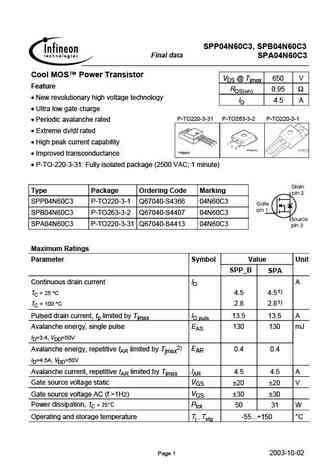
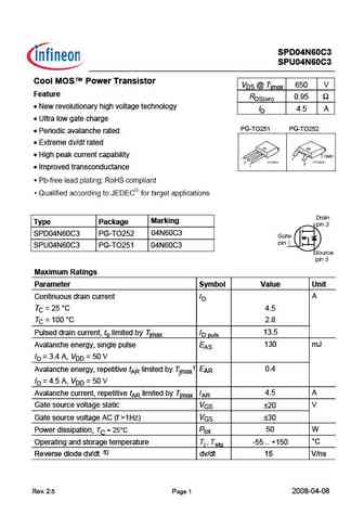
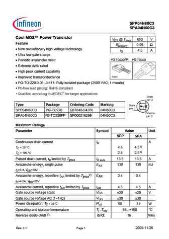
SPP04N60C3, SPB04N60C3 Final data SPA04N60C3 Cool MOS Power Transistor VDS @ Tjmax 650 V Feature RDS(on) 0.95 New revolutionary high voltage technology ID 4.5 A Ultra low gate charge P-TO220-3-31 P-TO263-3-2 P-TO220-3-1 Periodic avalanche rated Extreme dv/dt rated 3 High peak current capability 2 1 P-TO220-3-31 Improved transconductance P-TO
9.6. Size:678K infineon
spw24n60cfd.pdf 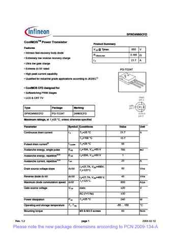
SPW24N60CFD TM C IMOSTM "9@/; %;+877+;B Features V 1?B6M 650 V !0 V &CIG>CH>8 ;6HI G 8DK GN 7D9N 9>D9 R 0.185 DS(on) max V "MIG B AN ADL G K GH G 8DK GN 8=6G;> 9 688DG9>CC
9.7. Size:807K infineon
spw24n60c3.pdf 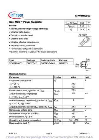
SPW24N60C3 Cool MOS Power Transistor VDS @ Tjmax 650 V Feature RDS(on) 0.16 New revolutionary high voltage technology ID 24.3 A Ultra low gate charge PG-TO247 Periodic avalanche rated Extreme dv/dt rated Ultra low effective capacitances Improved transconductance Type Package Ordering Code Marking SPW24N60C3 PG-TO247 Q67040-S4640 24N60C3 Maximum Rati
9.8. Size:539K infineon
spp24n60cfd.pdf 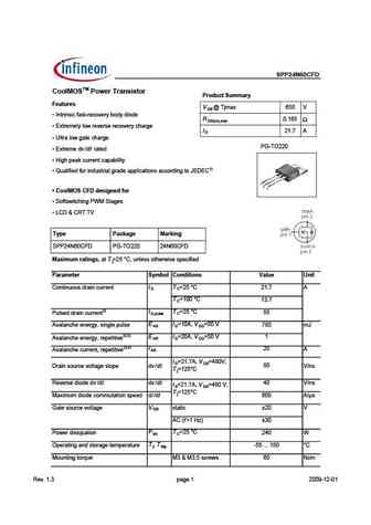
SPP24N60CFD CoolMOSTM Power Transistor Product Summary Features V @ Tjmax 650 V DS Intrinsic fast-recovery body diode R 0.185 DS(on),max Extremely low reverse recovery charge I 21.7 A D Ultra low gate charge PG-TO220 Extreme dv /dt rated High peak current capability Qualified for industrial grade applications according to JEDEC1) CoolMOS CFD designed
9.9. Size:620K infineon
sps04n60c3.pdf 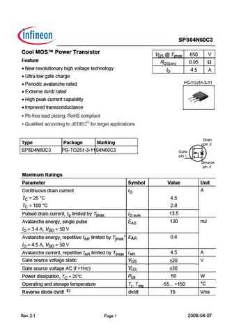
S VDS Tjmax G -3-11 Marking S G 1-3-11
9.11. Size:101K ixys
ixgh24n60cd1.pdf 
IXGH 24N60CD1 VCES = 600 V HiPerFASTTM IGBT IXGT 24N60CD1 IC25 = 48 A with Diode VCE(sat) = 2.5 V Lightspeed Series Preliminary data TO-268 Symbol Test Conditions Maximum Ratings (IXGT) VCES TJ = 25 C to 150 C 600 V VCGR TJ = 25 C to 150 C; RGE = 1 MW 600 V G VGES Continuous 20 V E C (TAB) VGEM Transient 30 V IC25 TC = 25 C48 A TO-247 AD (IXGH) IC110 TC = 110 C24 A
9.12. Size:98K ixys
ixgp24n60c.pdf 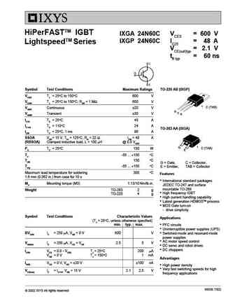
HiPerFASTTM IGBT IXGA 24N60C VCES = 600 V IXGP 24N60C IC25 = 48 A LightspeedTM Series VCE(sat)typ = 2.1 V tfi typ = 60 ns Symbol Test Conditions Maximum Ratings TO-220 AB (IXGP) VCES TJ = 25 C to 150 C 600 V VCGR TJ = 25 C to 150 C; RGE = 1 M 600 V C (TAB) VGES Continuous 20 V G C VGEM Transient 30 V E IC25 TC = 25 C48 A IC110 TC = 110 C24 A TO-263 AA (IXGA) ICM TC
9.13. Size:92K ixys
ixgp24n60c4.pdf 
Advance Technical Information High-Gain IGBTs VCES = 600V IXGP24N60C4 IC110 = 24A IXGH24N60C4 VCE(sat) 2.70V tfi(typ) = 68ns High-Speed PT Trench IGBTs TO-220AB (IXGP) Symbol Test Conditions Maximum Ratings VCES TJ = 25 C to 150 C 600 V G C Tab VCGR TJ = 25 C to 150 C, RGE = 1M 600 V E VGES Continuous 20 V VGEM Transient 30 V TO-247 AD (IX
9.14. Size:233K ixys
ixgh24n60c4d1.pdf 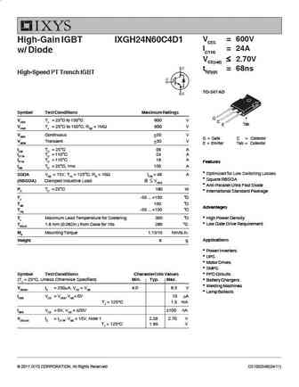
VCES = 600V High-Gain IGBT IXGH24N60C4D1 IC110 = 24A w/ Diode VCE(sat) 2.70V tfi(typ) = 68ns High-Speed PT Trench IGBT TO-247 AD Symbol Test Conditions Maximum Ratings G VCES TJ = 25 C to 150 C 600 V C Tab E VCGR TJ = 25 C to 150 C, RGE = 1M 600 V VGES Continuous 20 V G = Gate C = Collector VGEM Transient 30 V E = Emitter
9.15. Size:52K ixys
ixgt24n60c.pdf 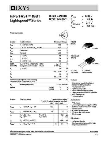
IXGH 24N60C VCES = 600 V HiPerFASTTM IGBT IXGT 24N60C IC25 = 48 A LightspeedTM Series VCE(sat)typ = 2.1 V tfi typ = 60 ns Preliminary data Symbol Test Conditions Maximum Ratings TO-268 (IXGT) VCES TJ = 25 C to 150 C 600 V G VCGR TJ = 25 C to 150 C; RGE = 1 MW 600 V C (TAB) E VGES Continuous 20 V VGEM Transient 30 V IC25 TC = 25 C48 A TO-247 AD (IXGH) IC110 TC = 110
9.16. Size:92K ixys
ixgh24n60c4.pdf 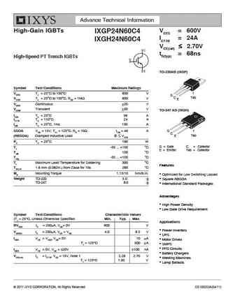
Advance Technical Information High-Gain IGBTs VCES = 600V IXGP24N60C4 IC110 = 24A IXGH24N60C4 VCE(sat) 2.70V tfi(typ) = 68ns High-Speed PT Trench IGBTs TO-220AB (IXGP) Symbol Test Conditions Maximum Ratings VCES TJ = 25 C to 150 C 600 V G C Tab VCGR TJ = 25 C to 150 C, RGE = 1M 600 V E VGES Continuous 20 V VGEM Transient 30 V TO-247 AD (IX
9.17. Size:98K ixys
ixga24n60c.pdf 
HiPerFASTTM IGBT IXGA 24N60C VCES = 600 V IXGP 24N60C IC25 = 48 A LightspeedTM Series VCE(sat)typ = 2.1 V tfi typ = 60 ns Symbol Test Conditions Maximum Ratings TO-220 AB (IXGP) VCES TJ = 25 C to 150 C 600 V VCGR TJ = 25 C to 150 C; RGE = 1 M 600 V C (TAB) VGES Continuous 20 V G C VGEM Transient 30 V E IC25 TC = 25 C48 A IC110 TC = 110 C24 A TO-263 AA (IXGA) ICM TC
9.18. Size:54K ixys
ixgr24n60c.pdf 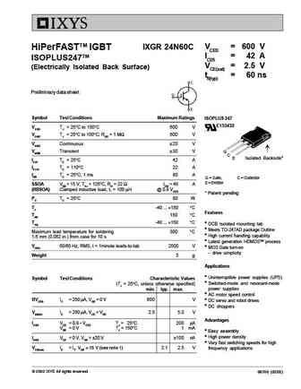
VCES = 600 V IXGR 24N60C HiPerFASTTM IGBT IC25 = 42 A ISOPLUS247TM VCE(sat) = 2.5 V (Electrically Isolated Back Surface) tfi(typ) = 60 ns Preliminary data sheet Symbol Test Conditions Maximum Ratings ISOPLUS 247 E153432 VCES TJ = 25 C to 150 C 600 V VCGR TJ = 25 C to 150 C; RGE = 1 M 600 V VGES Continuous 20 V VGEM Transient 30 V G C E Isolated Backside* IC25 TC =
9.19. Size:100K ixys
ixga24n60c ixgp24n60c.pdf 
HiPerFASTTM IGBT IXGA 24N60C VCES = 600 V IXGP 24N60C IC25 = 48 A LightspeedTM Series VCE(sat)typ = 2.1 V tfi typ = 60 ns Symbol Test Conditions Maximum Ratings TO-220 AB (IXGP) VCES TJ = 25 C to 150 C 600 V VCGR TJ = 25 C to 150 C; RGE = 1 M 600 V C (TAB) VGES Continuous 20 V G C VGEM Transient 30 V E IC25 TC = 25 C48 A IC110 TC = 110 C24 A TO-263 AA (IXGA) ICM TC
9.20. Size:52K ixys
ixgh24n60c.pdf 
IXGH 24N60C VCES = 600 V HiPerFASTTM IGBT IXGT 24N60C IC25 = 48 A LightspeedTM Series VCE(sat)typ = 2.1 V tfi typ = 60 ns Preliminary data Symbol Test Conditions Maximum Ratings TO-268 (IXGT) VCES TJ = 25 C to 150 C 600 V G VCGR TJ = 25 C to 150 C; RGE = 1 MW 600 V C (TAB) E VGES Continuous 20 V VGEM Transient 30 V IC25 TC = 25 C48 A TO-247 AD (IXGH) IC110 TC = 110
9.21. Size:84K ixys
ixgp24n60c4d1.pdf 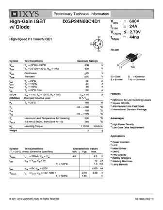
Preliminary Technical Information VCES = 600V High-Gain IGBT IXGP24N60C4D1 IC110 = 24A w/ Diode VCE(sat) 2.70V tfi(typ) = 44ns High-Speed PT Trench IGBT TO-220 Symbol Test Conditions Maximum Ratings G VCES TJ = 25 C to 150 C 600 V C Tab E VCGR TJ = 25 C to 150 C, RGE = 1M 600 V VGES Continuous 20 V VGEM Transient 30 V G = Gate C = Collector
9.22. Size:101K ixys
ixgt24n60cd1.pdf 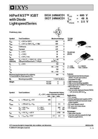
IXGH 24N60CD1 VCES = 600 V HiPerFASTTM IGBT IXGT 24N60CD1 IC25 = 48 A with Diode VCE(sat) = 2.5 V Lightspeed Series Preliminary data TO-268 Symbol Test Conditions Maximum Ratings (IXGT) VCES TJ = 25 C to 150 C 600 V VCGR TJ = 25 C to 150 C; RGE = 1 MW 600 V G VGES Continuous 20 V E C (TAB) VGEM Transient 30 V IC25 TC = 25 C48 A TO-247 AD (IXGH) IC110 TC = 110 C24 A
9.23. Size:128K ixys
ixga24n60c4.pdf 
Advance Technical Information High-Gain IGBTs VCES = 600V IXGA24N60C4 IC110 = 24A IXGP24N60C4 VCE(sat) 2.70V IXGH24N60C4 tfi(typ) = 68ns High-Speed PT Trench IGBTs TO-263 (IXGA) G E C (Tab) TO-220 (IXGP) Symbol Test Conditions Maximum Ratings VCES TJ = 25 C to 150 C 600 V VCGR TJ = 25 C to 150 C, RGE = 1M 600 V VGES Continuous 20 V G C C (
9.24. Size:477K taiwansemi
tsm4n60ch tsm4n60ci tsm4n60cp tsm4n60cz.pdf 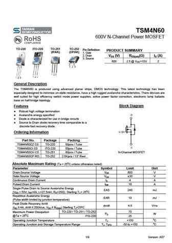
TSM4N60 600V N-Channel Power MOSFET TO-220 ITO-220 TO-251 TO-252 Pin Definition PRODUCT SUMMARY (IPAK) (DPAK) 1. Gate 2. Drain VDS (V) RDS(on)( ) ID (A) 3. Source 600 2.5 @ VGS =10V 2 General Description The TSM4N60 is produced using advanced planar stripe, DMOS technology. This latest technology has been especially designed to minimize on-state resistance, have a
9.25. Size:379K sisemi
sif4n60c.pdf 
Shenzhen SI Semiconductors Co., LTD. Product Specification Shenzhen SI Semiconductors Co., LTD. Product Specification Shenzhen SI Semiconductors Co., LTD. Product Specification Shenzhen SI Semiconductors Co., LTD. Product Specification N- MOS / N-CHANNEL POWER MOSFET SIF4N60C N- MOS / N-CHANNEL POWER MOSFET SIF4N60C N- MOS / N-CHANN
9.26. Size:382K sisemi
sif4n60c 1.pdf 
Shenzhen SI Semiconductors Co., LTD. Product Specification Shenzhen SI Semiconductors Co., LTD. Product Specification Shenzhen SI Semiconductors Co., LTD. Product Specification Shenzhen SI Semiconductors Co., LTD. Product Specification N- MOS / N-CHANNEL POWER MOSFET SIF4N60C N- MOS / N-CHANNEL POWER MOSFET SIF4N60C N- MOS / N-CHANN
9.28. Size:255K inpower semi
ftp04n60c fta04n60c.pdf 
FTP04N60C FTA04N60C N-Channel MOSFET Pb Lead Free Package and Finish Applications VDSS RDS(ON) (Max.) ID Adaptor Charger 600 V 2.2 4.0 A SMPS Standby Power Features D RoHS Compliant Low ON Resistance Low Gate Charge Peak Current vs Pulse Width Curve Inductive Switching Curves G G G Ordering Information DS DS TO-220F TO-220 S PART
9.29. Size:144K jdsemi
cm4n60c.pdf 
R CM4N60C www.jdsemi.cn ShenZhen Jingdao Electronic Co.,Ltd. POWER MOSFET 600V N-Channel VDMOS RoHS
9.30. Size:144K jdsemi
cm4n60c to251.pdf 
R CM4N60C www.jdsemi.cn ShenZhen Jingdao Electronic Co.,Ltd. POWER MOSFET 600V N-Channel VDMOS RoHS
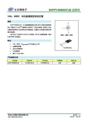
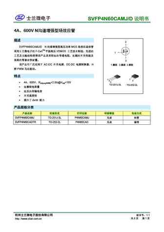
9.34. Size:318K silan
svfp14n60cfj.pdf 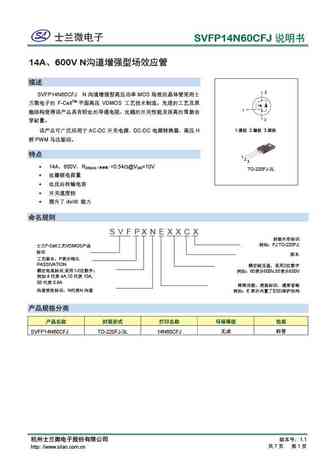
SVFP14N60CFJ 14A 600V N 2 SVFP14N60CFJ N MOS F-CellTM VDMOS 1 3 1. 2.
9.35. Size:323K silan
svf4n60cafj.pdf 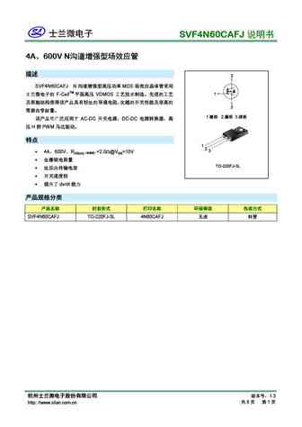
SVF4N60CAFJ 4A 600V N 2 SVF4N60CAFJ N MOS 1 F-CellTM VDMOS 3 1. 2.
9.37. Size:561K bruckewell
ms4n60c.pdf 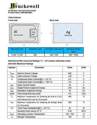
HV MOSFET DIE SPECIFICATION Product Name BW-MS4N60C Chip Features Front side Back side Chip Size (um) Thickness (um) Pad Size-Gate (um) Pad Size-Source (um) 3,180 * 2,720 350 420 * 520 900 * 1900 Referenced PKG Electrical Ratings TC = 25 Cunless otherwise noted Absolute Maximum Ratings Symbol Parameter Value Units VDSS Drain to Source Voltage 600 V VGS Gate to Source Vol
9.38. Size:670K way-on
wml14n60c4 wmk14n60c4 wmm14n60c4 wmn14n60c4 wmp14n60c4 wmo14n60c4.pdf 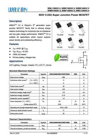
WML1 MM14N60C 14N60C4, WMK14N60C4, WM C4 WMN14N60C4, WMP14N60C4, WM C4 MO14N60C 600V n Power MOSFET V 0.33 Super Junction Descrip ption WMOSTM C4 is Wa 4th generation super ayon s n junction MOSFET fa that is utilizing charge M amily S balance te or extremely esistance echnology fo y low on-re D S D G G G S D G and low ga charge performanc WMOSTM C4
9.39. Size:853K cn vbsemi
spu04n60c3.pdf 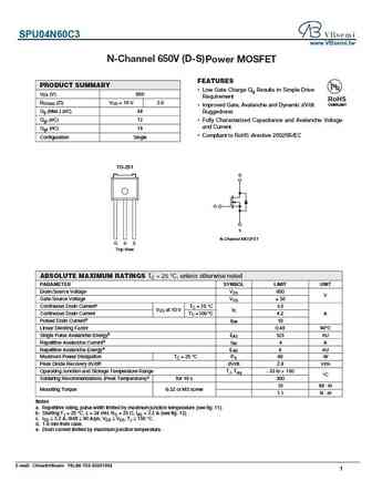
SPU04N60C3 www.VBsemi.tw N hannel 650 D S Power MOSFET FEATURES PRODUCT SUMMARY Low Gate Charge Qg Results in Simple Drive VDS (V) 650 Requirement RoHS RDS(on) ( )VGS = 10 V 2.0 COMPLIANT Improved Gate, Avalanche and Dynamic dV/dt Qg (Max.) (nC) 48 Ruggedness Qgs (nC) 12 Fully Characterized Capacitance and Avalanche Voltage and Current Qgd (nC) 19 Compli
9.40. Size:247K inchange semiconductor
spp24n60c3.pdf 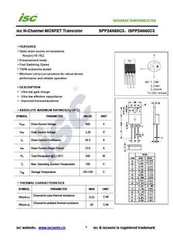
isc N-Channel MOSFET Transistor SPP24N60C3 ISPP24N60C3 FEATURES Static drain-source on-resistance RDS(on) 0.16 Enhancement mode Fast Switching Speed 100% avalanche tested Minimum Lot-to-Lot variations for robust device performance and reliable operation DESCRIPTION Ultra low gate charge Ultra low effective capacitance Improved transconductance ABSO
9.41. Size:248K inchange semiconductor
spp04n60c3.pdf 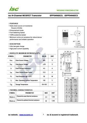
isc N-Channel MOSFET Transistor SPP04N60C3 ISPP04N60C3 FEATURES Static drain-source on-resistance RDS(on) 0.95 Enhancement mode Fast Switching Speed 100% avalanche tested Minimum Lot-to-Lot variations for robust device performance and reliable operation DESCRIPTION Ultra low gate charge High peak current capability ABSOLUTE MAXIMUM RATINGS(T =25 ) a
9.42. Size:258K inchange semiconductor
spb04n60c3.pdf 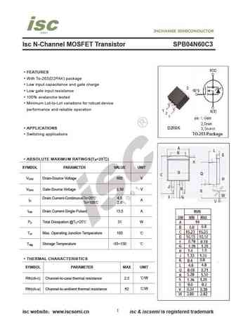
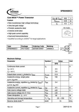
Isc N-Channel MOSFET Transistor SPB04N60C3 FEATURES With To-263(D2PAK) package Low input capacitance and gate charge Low gate input resistance 100% avalanche tested Minimum Lot-to-Lot variations for robust device performance and reliable operation APPLICATIONS Switching applications ABSOLUTE MAXIMUM RATINGS(T =25 ) a SYMBOL PARAMETER VALUE UNIT V Drain-Source Vo
9.43. Size:208K inchange semiconductor
spu04n60c3.pdf 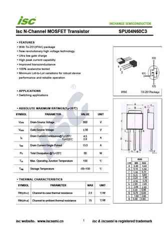
INCHANGE Semiconductor Isc N-Channel MOSFET Transistor SPU04N60C3 FEATURES With To-251(IPAK) package New revolutionary high voltage technology Ultra low gate charge High peak current capability Improved transconductance 100% avalanche tested Minimum Lot-to-Lot variations for robust device performance and reliable operation APPLICATIONS Switching applications A
9.44. Size:244K inchange semiconductor
spw24n60cfd.pdf 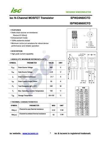
isc N-Channel MOSFET Transistor SPW24N60CFD ISPW24N60CFD FEATURES Static drain-source on-resistance RDS(on) 185m Enhancement mode 100% avalanche tested Minimum Lot-to-Lot variations for robust device performance and reliable operation DESCRITION High peak current capability ABSOLUTE MAXIMUM RATINGS(T =25 ) a SYMBOL PARAMETER VALUE UNIT V Drain-Source Volta
9.45. Size:244K inchange semiconductor
spw24n60c3.pdf 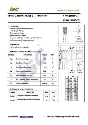
isc N-Channel MOSFET Transistor SPW24N60C3 ISPW24N60C3 FEATURES Static drain-source on-resistance RDS(on) 160m Enhancement mode 100% avalanche tested Minimum Lot-to-Lot variations for robust device performance and reliable operation DESCRITION High peak current capability ABSOLUTE MAXIMUM RATINGS(T =25 ) a SYMBOL PARAMETER VALUE UNIT V Drain-Source Voltage
9.46. Size:247K inchange semiconductor
spp24n60cfd.pdf 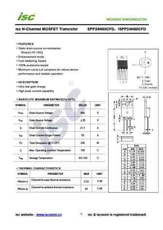
isc N-Channel MOSFET Transistor SPP24N60CFD ISPP24N60CFD FEATURES Static drain-source on-resistance RDS(on) 0.185 Enhancement mode Fast Switching Speed 100% avalanche tested Minimum Lot-to-Lot variations for robust device performance and reliable operation DESCRIPTION Ultra low gate charge High peak current capability ABSOLUTE MAXIMUM RATINGS(T =25 )
9.47. Size:245K inchange semiconductor
spd04n60c3.pdf 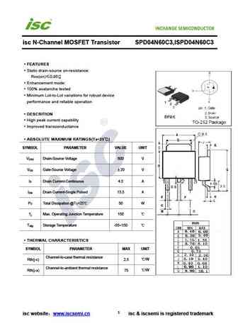
isc N-Channel MOSFET Transistor SPD04N60C3,ISPD04N60C3 FEATURES Static drain-source on-resistance RDS(on) 0.95 Enhancement mode 100% avalanche tested Minimum Lot-to-Lot variations for robust device performance and reliable operation DESCRITION High peak current capability Improved transconductance ABSOLUTE MAXIMUM RATINGS(T =25 ) a SYMBOL PARAMETER VALUE
Другие MOSFET... IPI45N04S4L-08
, IPP45N04S4L-08
, TP2301PR
, TP2302NR
, TP2305PR
, TP3443PR
, TP4812NR
, TP9435PR
, STF13NM60N
, AON6786
, AON6790
, AP9918H
, AP9918J
, CEB7030L
, CEP7030L
, CSD30N55
, DMT10N60
.