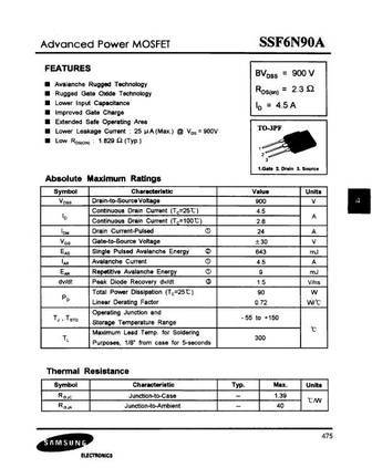
SSF6N90A. Аналоги и основные параметры
Наименование производителя: SSF6N90A
Тип транзистора: MOSFET
Полярность: N
Предельные значения
Pd ⓘ
- Максимальная рассеиваемая мощность: 90 W
|Vds|ⓘ - Максимально допустимое напряжение сток-исток: 900 V
|Vgs|ⓘ - Максимально допустимое напряжение затвор-исток: 30 V
|Id| ⓘ - Максимально допустимый постоянный ток стока: 4.5 A
Tj ⓘ - Максимальная температура канала: 150 °C
Электрические характеристики
tr ⓘ -
Время нарастания: 40 ns
Cossⓘ - Выходная емкость: 135 pf
RDSonⓘ - Сопротивление сток-исток открытого транзистора: 2.3 Ohm
Тип корпуса: TO3PF
Аналог (замена) для SSF6N90A
- подборⓘ MOSFET транзистора по параметрам
SSF6N90A даташит
9.1. Size:263K 1
ssf6n80a.pdf 
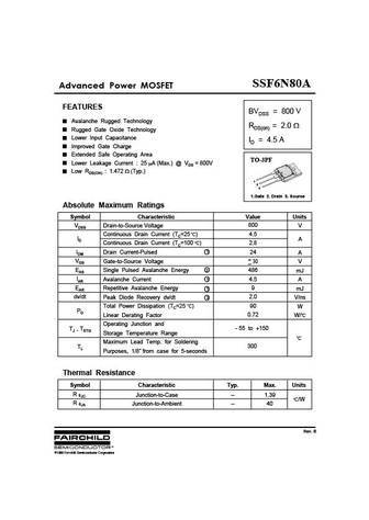
SSF6N80A Advanced Power MOSFET FEATURES BVDSS = 800 V Avalanche Rugged Technology RDS(on) = 2.0 Rugged Gate Oxide Technology Lower Input Capacitance ID = 4.5 A Improved Gate Charge Extended Safe Operating Area TO-3PF Lower Leakage Current 25 A (Max.) @ VDS = 800V Low RDS(ON) 1.472 (Typ.) 1 2 3 1.Gate 2. Drain 3. Source Absolute Maximum Ratings Symbol Cha
9.3. Size:532K silikron
ssf6n80f.pdf 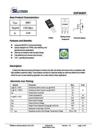
SSF6N80F Main Product Characteristics VDSS 800V RDS(on) 2.2 (typ.) ID 5.5A Marking a nd p in Sche ma ti c di agr a m TO220F Assignment Features and Benefits Advanced MOSFET process technology Special designed for PWM, load switching and general purpose applications Ultra low on-resistance with low gate charge Fast switching and reverse body reco
9.5. Size:443K silikron
ssf6n60g.pdf 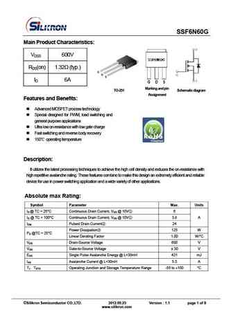
SSF6N60G Main Product Characteristics VDSS 600V RDS(on) 1.32 (typ.) ID 6A TO-251 Marking a nd p in Sche ma ti c di agr a m Assignment Features and Benefits Advanced MOSFET process technology Special designed for PWM, load switching and general purpose applications Ultra low on-resistance with low gate charge Fast switching and reverse body recovery
9.6. Size:407K silikron
ssf6ns70ugx.pdf 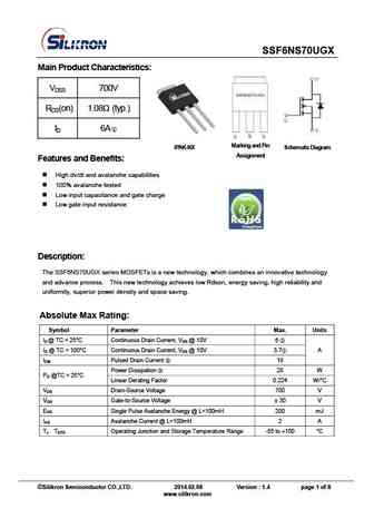
SSF6NS70UGX Main Product Characteristics VDSS 700V RDS(on) 1.08 (typ.) ID 6A IPAK-NX Marking and Pi n Schematic Diagram Assignment Features and Benefits High dv/dt and avalanche capabilities 100% avalanche tested Low input capacitance and gate charge Low gate input resistance Description The SSF6NS70UGX series MOSFETs is a new technology, whi
9.7. Size:411K silikron
ssf6n70gm.pdf 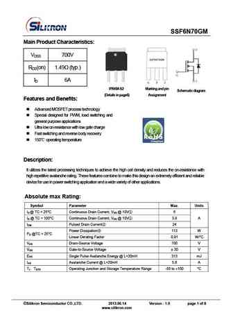
SSF6N70GM Main Product Characteristics VDSS 700V RDS(on) 1.49 (typ.) ID 6A IPAKM-S2 Marking and p in S che ma ti c di ag ra m (Details in page6) Assignment Features and Benefits Advanced MOSFET process technology Special designed for PWM, load switching and general purpose applications Ultra low on-resistance with low gate charge Fast switching and
9.8. Size:451K silikron
ssf6n70g.pdf 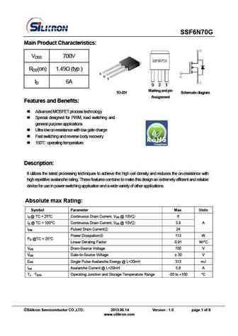
SSF6N70G Main Product Characteristics VDSS 700V RDS(on) 1.49 (typ.) ID 6A TO-251 Marking and p in S che ma ti c di ag ra m Assignment Features and Benefits Advanced MOSFET process technology Special designed for PWM, load switching and general purpose applications Ultra low on-resistance with low gate charge Fast switching and reverse body recovery
9.9. Size:457K silikron
ssf6ns70ug.pdf 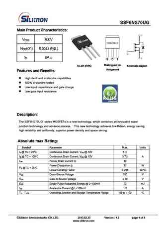
SSF6NS70UG Main Product Characteristics VDSS 700V RDS(on) 0.95 (typ.) ID 6A TO-251 (IPAK) Marking and p in Schematic diagram Assignment Features and Benefits High dv/dt and avalanche capabilities 100% avalanche tested Low input capacitance and gate charge Low gate input resistance Description The SSF6NS70UG series MOSFETs is a new technology,
9.10. Size:478K silikron
ssf6n80g.pdf 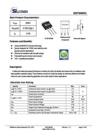
SSF6N80G Main Product Characteristics VDSS 800V RDS(on) 2.35 (typ.) ID 5.5A Marking and p in TO-251 (IPAK) Schematic diagram Assignment Features and Benefits Advanced MOSFET process technology Special designed for PWM, load switching and general purpose applications Ultra low on-resistance with low gate charge Fast switching and reverse body recov
9.11. Size:453K silikron
ssf6ns65uf.pdf 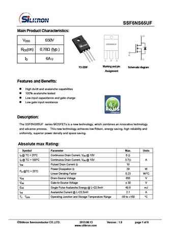
SSF6NS65UF Main Product Characteristics VDSS 650V RDS(on) 0.78 (typ.) ID 6A Marking and pin TO-220F Schematic diagram Assignment Features and Benefits High dv/dt and avalanche capabilities 100% avalanche tested Low input capacitance and gate charge Low gate input resistance Description The SSF6NS65UF series MOSFETs is a new technology, whic
9.12. Size:555K silikron
ssf6n40d.pdf 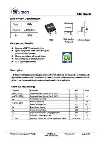
SSF6N40D Main Product Characteristics VDSS 400V RDS(on) 0.85 (typ.) ID 5.5A TO-252 Marking a nd p in Sche ma ti c di agr a m Assignment Features and Benefits Advanced MOSFET process technology Special designed for PWM, load switching and general purpose applications Ultra low on-resistance with low gate charge Fast switching and reverse body recover
9.13. Size:465K silikron
ssf6ns70ud.pdf 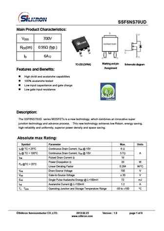
SSF6NS70UD Main Product Characteristics VDSS 700V RDS(on) 0.95 (typ.) ID 6A TO-252 (DPAK) Marking and p in Schematic diagram Assignment Features and Benefits High dv/dt and avalanche capabilities 100% avalanche tested Low input capacitance and gate charge Low gate input resistance Description The SSF6NS70UD series MOSFETs is a new technology,
9.14. Size:450K silikron
ssf6ns70ugs.pdf 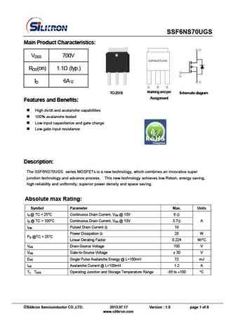
SSF6NS70UGS Main Product Characteristics VDSS 700V RDS(on) 1.1 (typ.) ID 6A TO-251S Marking and p in Schematic diagram Assignment Features and Benefits High dv/dt and avalanche capabilities 100% avalanche tested Low input capacitance and gate charge Low gate input resistance Description The SSF6NS70UGS series MOSFETs is a new technology, whic
9.15. Size:543K silikron
ssf6ns70g-d-f.pdf 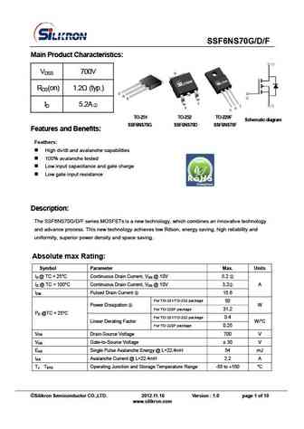
SSF6NS70G/D/F Main Product Characteristics VDSS 700V RDS(on) 1.2 (typ.) ID 5.2A 251 TO-252 TO- TO-220F Schematic diagram SSF6NS70G SSF6NS70D SSF6NS70F Features and Benefits Feathers High dv/dt and avalanche capabilities 100% avalanche tested Low input capacitance and gate charge Low gate input resistance Description The SSF6NS70G/D/F
Другие MOSFET... SSF25N40A
, SSF45N20A
, SSF4N80AS
, SSF4N90AS
, SSF5N80A
, SSF5N90A
, SSF6N70A
, SSF6N80A
, AOD4184A
, SSF70N10A
, SSF7N60A
, SSF7N80A
, SSF7N90A
, SSF80N06A
, SSF8N80A
, SSF8N90A
, SSF9N80A
.
History: BUZ72A