2312. Аналоги и основные параметры
Наименование производителя: 2312
Тип транзистора: MOSFET
Полярность: N
Предельные значения
Pd ⓘ - Максимальная рассеиваемая мощность: 1.25 W
|Vds|ⓘ - Максимально допустимое напряжение сток-исток: 20 V
|Vgs|ⓘ - Максимально допустимое напряжение затвор-исток: 10 V
|Id| ⓘ - Максимально допустимый постоянный ток стока: 6.8 A
Tj ⓘ - Максимальная температура канала: 150 °C
Электрические характеристики
tr ⓘ - Время нарастания: 18 ns
Cossⓘ - Выходная емкость: 300 pf
RDSonⓘ - Сопротивление сток-исток открытого транзистора: 0.021 Ohm
Тип корпуса: SOT-23
Аналог (замена) для 2312
- подборⓘ MOSFET транзистора по параметрам
2312 даташит
2312.pdf
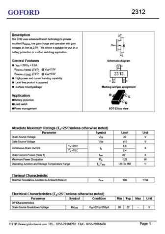
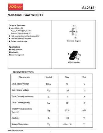
2312 GOFORD Description D The 2312 uses advanced trench technology to provide excellent RDS(ON), low gate charge and operation with gate G voltages as low as 2.5V. This device is suitable for use as a battery protection or in other switching application. S Schematic diagram General Features VDS = 20V,ID = 6.8A RDS(ON) @ VGS=2.5V =18m (TYP) RDS(ON) @ VGS=4.5V (TY
rn2312-rn2313.pdf
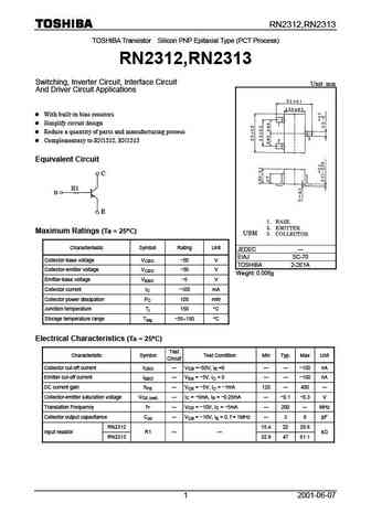
RN2312,RN2313 TOSHIBA Transistor Silicon PNP Epitaxial Type (PCT Process) RN2312,RN2313 Switching, Inverter Circuit, Interface Circuit Unit mm And Driver Circuit Applications With built-in bias resistors Simplify circuit design Reduce a quantity of parts and manufacturing process Complementary to RN1312, RN1313 Equivalent Circuit Maximum Ratings (Ta = 25 C)
2sk2312.pdf
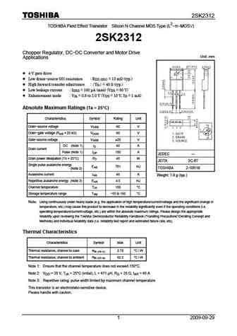
2SK2312 2 TOSHIBA Field Effect Transistor Silicon N Channel MOS Type (L - -MOSV) 2SK2312 Chopper Regulator, DC-DC Converter and Motor Drive Unit mm Applications 4-V gate drive Low drain-source ON resistance RDS (ON) = 13 m (typ.) High forward transfer admittance Yfs = 40 S (typ.) Low leakage current IDSS = 100 A (max) (VDS = 60 V) Enhancement mode
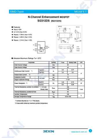
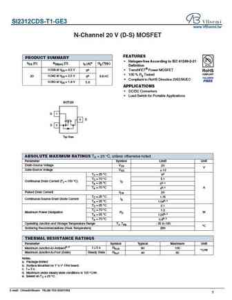
si2312cds.pdf
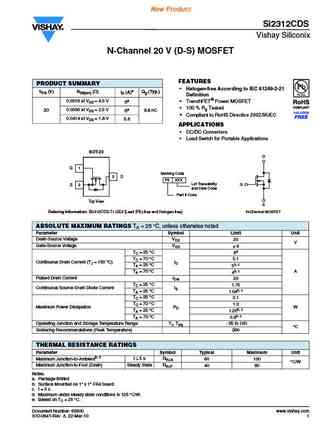
New Product Si2312CDS Vishay Siliconix N-Channel 20 V (D-S) MOSFET FEATURES PRODUCT SUMMARY Halogen-free According to IEC 61249-2-21 VDS (V) RDS(on) ( ) ID (A)e Qg (Typ.) Definition 0.0318 at VGS = 4.5 V TrenchFET Power MOSFET 6a 100 % Rg Tested 20 0.0356 at VGS = 2.5 V 6a 8.8 nC Compliant to RoHS Directive 2002/95/EC 0.0414 at VGS = 1.8 V 5.6 APPLI
si2312bds.pdf
Si2312BDS Vishay Siliconix N-Channel 20 V (D-S) MOSFET FEATURES PRODUCT SUMMARY Halogen-free According to IEC 61249-2-21 VDS (V) RDS(on) ( )ID (A) Qg (Typ.) Definition 0.031 at VGS = 4.5 V 5.0 TrenchFET Power MOSFET 20 0.037 at VGS = 2.5 V 4.6 7.5 100 % Rg Tested 0.047 at VGS = 1.8 V 4.1 Compliant to RoHS Directive 2002/95/EC TO-236 (SOT-23) G 1 3 D S 2
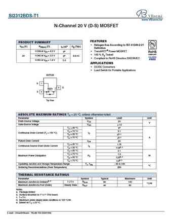
si2312ds.pdf
Si2312DS Vishay Siliconix N-Channel 20 -V (D-S) MOSFET FEATURES PRODUCT SUMMARY D 1.8-V Rated D RoHS Compliant VDS (V) rDS(on) (W) ID (A) Qg (Typ) Pb-free 0.033 @ VGS = 4.5 V 4.9 Available 0.040 @ VGS = 2.5 V 4.4 20 11.2 0.051 @ VGS = 1.8 V 3.9 TO-236 (SOT-23) G 1 3 D S 2 Top View Si2312DS (C2)* *Marking Code Ordering Information Si2312DS-T1 Si2312DS-T1 E3 (Lead (Pb)-F
mtm23123.pdf
MTM23123 Silicon P-channel MOSFET For switching Overview Package MTM23123 is P-channel MOS FET for load switch circuits. Code SMini3-G1-B Features Pin Name Low voltage drive (2.5 V, 4 V) 1 Gate Realization of low on-resistance, using extremely fine process 2 Source Contributes to miniaturization of sets, reduction of component count. 3 Drain E
ut2312.pdf
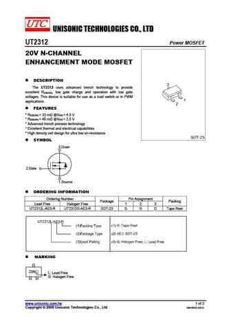
UNISONIC TECHNOLOGIES CO., LTD UT2312 Power MOSFET 20V N-CHANNEL ENHANCEMENT MODE MOSFET DESCRIPTION The UT2312 uses advanced trench technology to provide excellent RDS(ON), low gate charge and operation with low gate voltages. This device is suitable for use as a load switch or in PWM applications. FEATURES * RDS(ON) = 33 m @VGS = 4.5 V * RDS(ON) = 40 m @VGS = 2
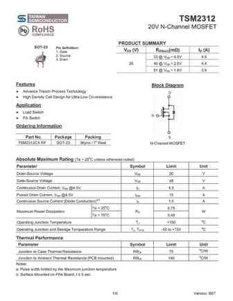
tsm2312cx.pdf
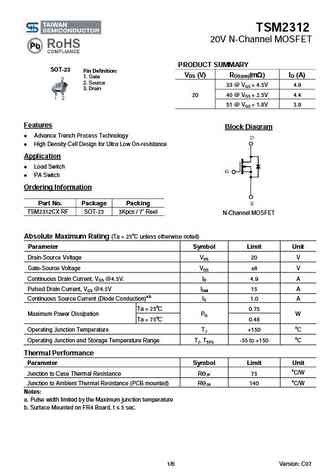
TSM2312 20V N-Channel MOSFET PRODUCT SUMMARY SOT-23 Pin Definition VDS (V) RDS(on)(m ) ID (A) 1. Gate 2. Source 33 @ VGS = 4.5V 4.9 3. Drain 20 40 @ VGS = 2.5V 4.4 51 @ VGS = 1.8V 3.9 Features Block Diagram Advance Trench Process Technology High Density Cell Design for Ultra Low On-resistance Application Load Switch PA Switch Ordering In
cj2312.pdf
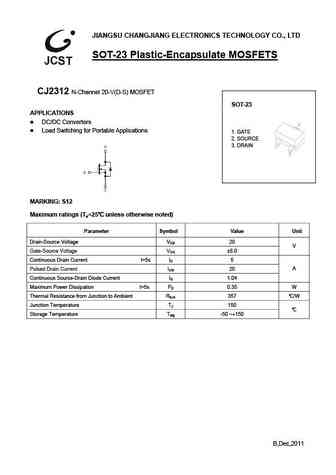
JIANGSU CHANGJIANG ELECTRONICS TECHNOLOGY CO., LTD SOT-23 Plastic-Encapsulate MOSFETS CJ2312 N-Channel 20-V(D-S) MOSFET SOT-23 APPLICATIONS DC/DC Converters Load Switching for Portable Applications 1. GATE 2. SOURCE 3. DRAIN MARKING S12 Maximum ratings (Ta=25 unless otherwise noted) Parameter Symbol Value Unit Drain-Source Voltage VDS 20 V Gate-Source Volt
si2312.pdf
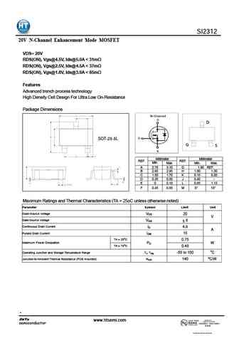
SI2312 20V N-Channel Enhancement Mode MOSFET VDS= 20V RDS(ON), Vgs@4.5V, Ids@5.0A
ces2312.pdf
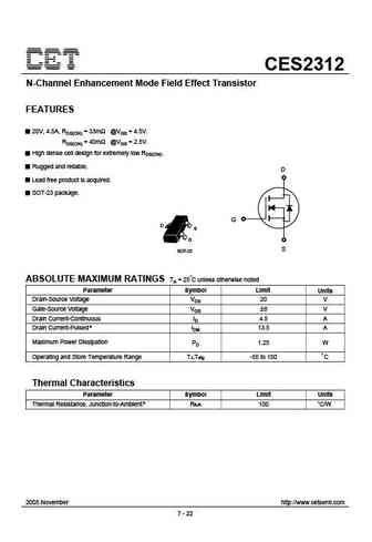
CES2312 N-Channel Enhancement Mode Field Effect Transistor FEATURES 20V, 4.5A, RDS(ON) = 33m @VGS = 4.5V. RDS(ON) = 40m @VGS = 2.5V. High dense cell design for extremely low RDS(ON). Rugged and reliable. D Lead free product is acquired. SOT-23 package. G D S G S SOT-23 ABSOLUTE MAXIMUM RATINGS TA = 25 C unless otherwise noted Parameter Symbol Limit Units Drain-Source Vo
wtc2312.pdf
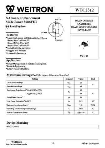
WTC2312 N-Channel Enhancement 3 DRAIN DRAIN CURRENT Mode Power MOSFET 4.9 AMPERES P b Lead(Pb)-Free DRAIN SOUCE VOLTAGE 20 VOLTAGE 1 GATE Features * Super High Dense Cell Design For Low RDS(ON) 2 SOURCE RDS(ON)
se2312.pdf
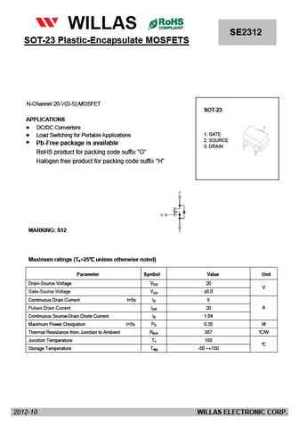
FM120-M WILLAS THRU SE2312 SOT-23 Plastic-Encapsulate MOSFETS FM1200-M 1.0A SURFACE MOUNT SCHOTTKY BARRIER RECTIFIERS -20V- 200V SOD-123 PACKAGE Pb Free Produc Package outline Features Batch process design, excellent power dissipation offers better reverse leakage current and thermal resistance. SOD-123H Low profile surface mounted application in order to optimiz
ap2312gn.pdf
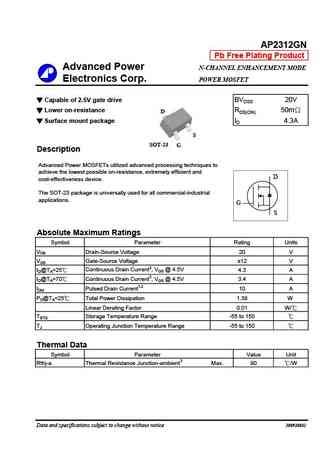
AP2312GN Pb Free Plating Product Advanced Power N-CHANNEL ENHANCEMENT MODE Electronics Corp. POWER MOSFET Capable of 2.5V gate drive BVDSS 20V Lower on-resistance RDS(ON) 50m D Surface mount package ID 4.3A S SOT-23 G Description Advanced Power MOSFETs utilized advanced processing techniques to achieve the lowest possible o
am2312n.pdf
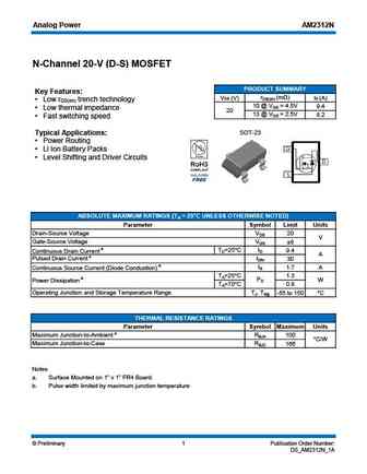
Analog Power AM2312N N-Channel 20-V (D-S) MOSFET PRODUCT SUMMARY Key Features rDS(on) (m ) VDS (V) ID (A) Low r trench technology DS(on) 10 @ VGS = 4.5V 9.4 Low thermal impedance 20 13 @ VGS = 2.5V 8.2 Fast switching speed Typical Applications SOT-23 Power Routing Li Ion Battery Packs Level Shifting and Driver Circuits ABSOLUTE MAXIMUM RATIN
afn2312.pdf
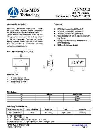
AFN2312 Alfa-MOS 20V N-Channel Technology Enhancement Mode MOSFET General Description Features AFN2312, N-Channel enhancement mode 20V/4.0A,RDS(ON)=36m @VGS=4.5V MOSFET, uses Advanced Trench Technology 20V/3.2A,RDS(ON)=40m @VGS=2.5V to provide excellent RDS(ON), low gate charge. 20V/2.8A,RDS(ON)=52m @VGS=1.8V These devices are particularly suited for low Supe
afn2312a.pdf
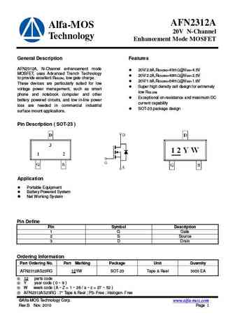
AFN2312A Alfa-MOS 20V N-Channel Technology Enhancement Mode MOSFET General Description Features AFN2312A, N-Channel enhancement mode 20V/2.8A,RDS(ON)=45m @VGS=4.5V MOSFET, uses Advanced Trench Technology 20V/2.2A,RDS(ON)=48m @VGS=2.5V to provide excellent RDS(ON), low gate charge. 20V/1.8A,RDS(ON)=64m @VGS=1.8V These devices are particularly suited for low Su
si2312.pdf
Shenzhen Tuofeng Semiconductor Technology Co., Ltd Si2312 PRODUCT SUMMARY VDS (V) rDS(on) (W) ID (A) Qg (Typ) 0.031 @ VGS = 4.5 V 5.0 0.037 @ VGS = 2.5 V 4.6 20 7.5 0.047 @ VGS = 1.8 V 4.1 (SOT-23) G 1 3 D Ordering Information Si2312 S 2 Top View ABSOLUTE MAXIMUM RATINGS (TA = 25_C UNLESS OTHERWISE NOTED) Parameter Symbol 5 sec Steady State Unit Drain-Source Voltage VDS 20 V
ssf2312.pdf
SSF2312 D DESCRIPTION The SSF2312 uses advanced trench technology to provide excellent RDS(ON), low gate charge and operation G with gate voltages as low as 2.5V. This device is suitable for use as a Battery protection or in other Switching application. S Schematic diagram GENERAL FEATURES D VDS = 20V,ID = 4.5A 3 RDS(ON)
ln2312lt1g s-ln2312lt1g.pdf
LESHAN RADIO COMPANY, LTD. 20V N-Channel Enhancement-Mode MOSFET VDS= 20V LN2312LT1G RDS(ON), Vgs@4.5V, Ids@5.0A = 41m S-LN2312LT1G RDS(ON), Vgs@2.5V, Ids@4.5A = 47m Features 3 Advanced trench process technology High Density Cell Design For Ultra Low On-Resistance 1 we declare that the material of product 2 compliance with RoHS requirements. SOT 23 (TO 236AB)
sm2312nsa.pdf
SM2312NSA N-Channel Enhancement Mode MOSFET Features Pin Description 30V/3A, D RDS(ON)=72m (max.) @ VGS=10V S RDS(ON)=100m (max.) @ VGS=4.5V G Reliable and Rugged Lead Free and Green Devices Available Top View of SOT-23-3 (RoHS Compliant) D Applications G DC-DC Conversion. Load Switch for PC fields. S Load Switch for Portables. N-Channel MOSFET Ordering and Marki
ftk2312.pdf
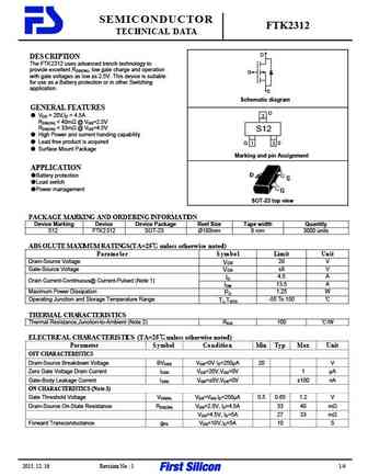
SEMICONDUCTOR FTK2312 TECHNICAL DATA D DESCRIPTION The FTK2312 uses advanced trench technology to provide excellent RDS(ON), low gate charge and operation G with gate voltages as low as 2.5V. This device is suitable for use as a Battery protection or in other Switching application. S Schematic diagram GENERAL FEATURES D VDS = 20V,ID = 4.5A 3 RDS(ON)
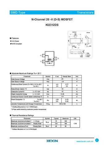
ki2312.pdf
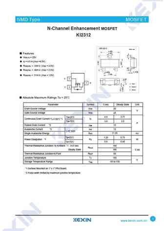
SMD Type MOSFET N-Channel Enhancement MOSFET KI2312 Features 3 VDS (V) = 20V ID = 4.9 A (VGS =4.5V) RDS(ON) 33m (VGS = 4.5V) 12 RDS(ON) 40m (VGS = 2.5V) RDS(ON) 51m (VGS = 1.8V) Absolute Maximum Ratings Ta = 25 Parameter Symbo
si2312ds-3.pdf
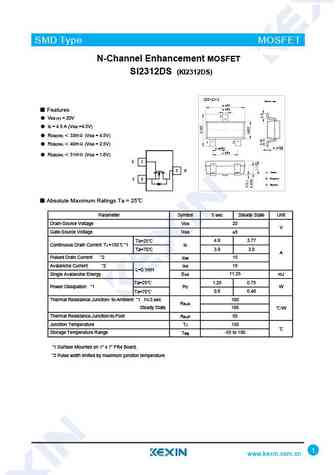
SMD Type MOSFET N-Channel Enhancement MOSFET SI2312DS (KI2312DS) SOT-23-3 Unit mm +0.2 2.9-0.1 +0.1 0.4 -0.1 Features 3 VDS (V) = 20V ID = 4.9 A (VGS =4.5V) RDS(ON) 33m (VGS = 4.5V) 1 2 RDS(ON) 40m (VGS = 2.5V) +0.02 +0.1 0.15 -0.02 0.95 -0.1 +0.1 1.9 -0.2 RDS(ON) 51m (VGS = 1.8V) G 1 3 D 1. Gate 2. Source S 2 3. Drain
si2312 ki2312.pdf
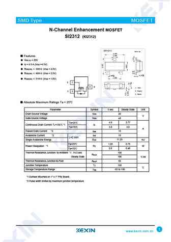
SMD Type MOSFET N-Channel Enhancement MOSFET SI2312 (KI2312) SOT-23-3 Unit mm +0.2 2.9-0.1 +0.1 0.4 -0.1 Features 3 VDS (V) = 20V ID = 4.9 A (VGS =4.5V) RDS(ON) 33m (VGS = 4.5V) 1 2 RDS(ON) 40m (VGS = 2.5V) +0.02 +0.1 0.15 -0.02 0.95 -0.1 +0.1 1.9 -0.2 RDS(ON) 51m (VGS = 1.8V) G 1 3 D 1. Gate 2. Source S 2 3. Drain Abs
ki2312ds.pdf
SMD Type Transistors N-Channel 20 -V (D-S) MOSFET KI2312DS SOT-23 Unit mm +0.1 2.9-0.1 +0.1 0.4-0.1 3 Features 1.8-V Rated RoHS Compliant 12 +0.1 +0.05 0.95-0.1 0.1-0.01 +0.1 1.9-0.1 1.Base 1. Gate 2.Emitter 2. Source 3. Drain 3.collector Absolute Maximum Ratings Ta = 25 Parameter Symbol 5 sec Steady State Unit Drain-Source Voltage VDS 20 V Gate-Source Voltage VGS 8
si2312ds.pdf
SMD Type MOSFET N-Channel Enhancement MOSFET SI2312DS (KI2312DS) SOT-23 Unit mm Features +0.1 2.9-0.1 +0.1 0.4 -0.1 VDS (V) = 20V 3 ID = 4.9 A (VGS =4.5V) RDS(ON) 33m (VGS = 4.5V) RDS(ON) 40m (VGS = 2.5V) 1 2 RDS(ON) 51m (VGS = 1.8V) +0.1 +0.05 0.95 -0.1 0.1 -0.01 1.9+0.1 -0.1 G 1 1.Gate 3 D 2.Source S 2 3.Drain Abs
cht2312gp.pdf
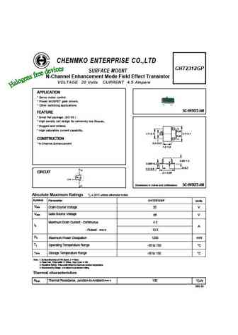
CHENMKO ENTERPRISE CO.,LTD CHT2312GP SURFACE MOUNT N-Channel Enhancement Mode Field Effect Transistor VOLTAGE 20 Volts CURRENT 4.5 Ampere APPLICATION * Servo motor control. * Power MOSFET gate drivers. * Other switching applications. SC-59/SOT-346 FEATURE * Small flat package. (SC-59 ) * High density cell design for extremely low RDS(ON). * Rugged and reliable. (2) * High sat
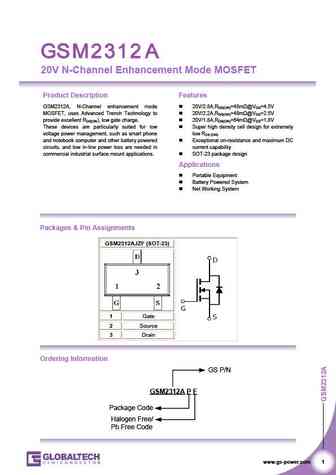
gsm2312.pdf
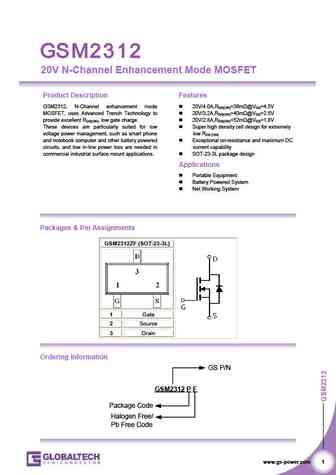
20V N-Channel Enhancement Mode MOSFET Product Description Features GSM2312, N-Channel enhancement mode 20V/4.0A,RDS(ON)=36m @VGS=4.5V MOSFET, uses Advanced Trench Technology to 20V/3.2A,RDS(ON)=40m @VGS=2.5V provide excellent RDS(ON), low gate charge. 20V/2.8A,RDS(ON)=52m @VGS=1.8V These devices are particularly suited for low Super high density cell design for e
gsm2312a.pdf
20V N-Channel Enhancement Mode MOSFET Product Description Features GSM2312A, N-Channel enhancement mode 20V/2.8A,RDS(ON)=45m @VGS=4.5V MOSFET, uses Advanced Trench Technology to 20V/2.2A,RDS(ON)=48m @VGS=2.5V provide excellent RDS(ON), low gate charge. 20V/1.8A,RDS(ON)=64m @VGS=1.8V These devices are particularly suited for low Super high density cell design for
me2312 me2312-g.pdf
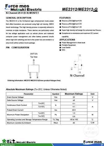
ME2312/ME2312-G N-Channel 20-V (D-S) MOSFET GENERAL DESCRIPTION FEATURES The ME2312-G is the N-Channel logic enhancement mode power RDS(ON) 33m @VGS=4.5V field effect transistors are produced using high cell density, DMOS RDS(ON) 40m @VGS=2.5V trench technology. This high density process is especially tailored to RDS(ON) 51m @VGS=1.8V minimize on-state resist
mmn2312.pdf
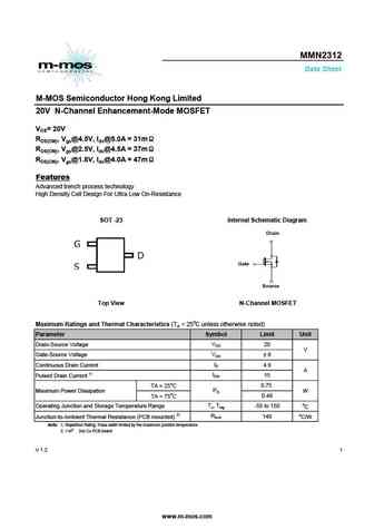
MMN2312 Data Sheet M-MOS Semiconductor Hong Kong Limited 20V N-Channel Enhancement-Mode MOSFET VDS= 20V RDS(ON), Vgs@4.5V, Ids@5.0A = 31m RDS(ON), Vgs@2.5V, Ids@4.5A = 37m RDS(ON), Vgs@1.8V, Ids@4.0A = 47m Features Advanced trench process technology High Density Cell Design For Ultra Low On-Resistance SOT -23 Internal Schematic Diagram Drain Gate Source Top View N-Cha
nce2312x.pdf
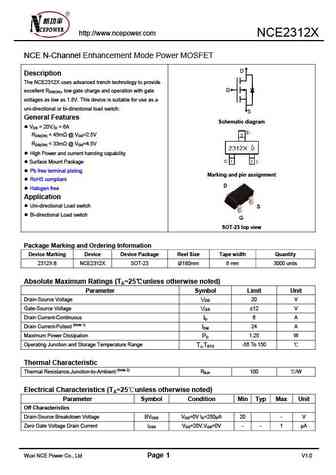
http //www.ncepower.com NCE2312X NCE N-Channel Enhancement Mode Power MOSFET D Description The NCE2312X uses advanced trench technology to provide G excellent RDS(ON), low gate charge and operation with gate voltages as low as 1.8V. This device is suitable for use as a uni-directional or bi-directional load switch. S General Features Schematic diagram VDS = 20V,ID = 6A
nce2312a.pdf
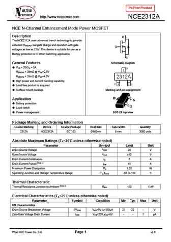
Pb Free Product http //www.ncepower.com NCE2312A NCE N-Channel Enhancement Mode Power MOSFET Description D The NCE2312A uses advanced trench technology to provide excellent RDS(ON), low gate charge and operation with gate G voltages as low as 2.5V. This device is suitable for use as a Battery protection or in other Switching application. S Schematic diagram General Features
nce2312.pdf
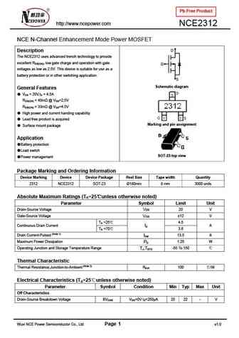
Pb Free Product http //www.ncepower.com NCE2312 NCE N-Channel Enhancement Mode Power MOSFET D Description The NCE2312 uses advanced trench technology to provide excellent RDS(ON), low gate charge and operation with gate G voltages as low as 2.5V. This device is suitable for use as a battery protection or in other switching application. S Schematic diagram General Features
pdn2312s.pdf
20V N-Channel MOSFETs PDN2312S General Description BVDSS RDSON ID These N-Channel enhancement mode power field effect transistors are using trench DMOS technology. This 20V 19m 6.7A advanced technology has been especially tailored to Features minimize on-state resistance, provide superior switching 20V, 6.7A, RDS(ON)=19m @VGS=4.5V performance, and withstand high ener
ssm2312gn.pdf
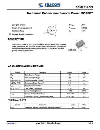
SSM2312GN N-channel Enhancement-mode Power MOSFET Low gate-charge BVDSS 20V D Simple drive requirement R 50m DS(ON) Fast switching ID 4.3A G Pb-free; RoHS compliant. S DESCRIPTION D The SSM2312GN is in a SOT-23-3 package, which is widely used for lower power commercial and industrial surface mount applications. This device is S suitable for low-voltage applications such as DC
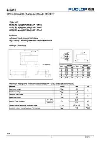
sl2312.pdf
SL2312 SOT-23 Package Information Dimensions in Millimeters Symbol MIN. MAX. A 0.900 1.150 A1 0.000 0.100 A2 0.900 1.050 b 0.300 0.500 c 0.080 0.150 D 2.800 3.000 E 1.200 1.400 E1 2.250 2.550 e 0.950TYP e1 1.800 2.000 L 0.550REF L1 0.300 0.500 0 8 www.slkormicro.com 3
si2312a.pdf
R UMW UMW SI2312A UMW SI2312A Features SOT 23 VDS (V) = 20V ID = 4.9 A (VGS =4.5V) RDS(ON) 33m (VGS = 4.5V) RDS(ON) 40m (VGS = 2.5V) RDS(ON) 51m (VGS = 1.8V) 1. GATE MARKING 2. SOURCE 3. DRAIN G 1 A12T 3 D S 2 Absolute Maximum Ratings Ta = 25 Parameter Symbol 5 sec Steady State Unit Drain-Source Voltage VDS 20 V Gate
atm2312nsa.pdf
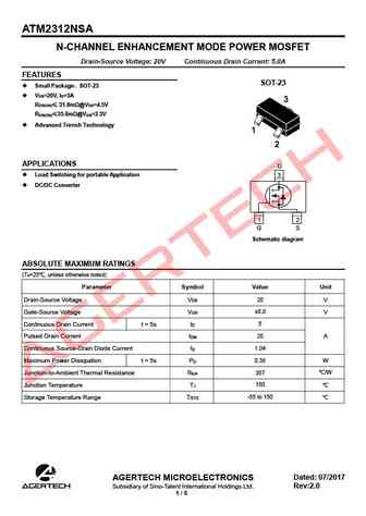
ATM2312NSA N-CHANNEL ENHANCEMENT MODE POWER MOSFET Drain-Source Voltage 20V Continuous Drain Current 5.0A FEATURES SOT-23 Small Package SOT-23 V =20V, I =5A DS D R 31.8m @V =4.5V DS(ON) GS R 35.6m @V =2.5V DS(ON) GS Advanced Trench Technology APPLICATIONS D Load Switching for portable Application 3 DC/DC Converter 1 2 G S Schematic d
as2312.pdf
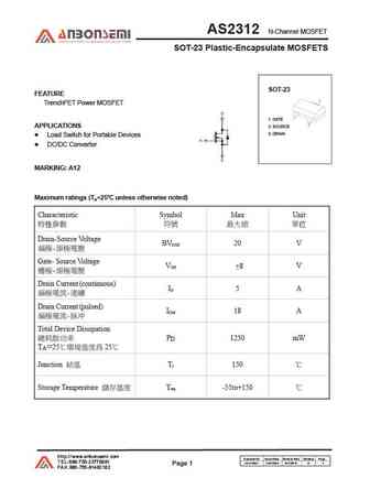
AS231 2 N-Channel MOSFET SOT-23 Plastic-Encapsulate MOSFETS Dimensions In Millimeters Dimensions In Inches Symbol Min Max Min Max A 0.900 1.150 0.035 0.045 A1 0.000 0.100 0.000 0.004 A2 0.900 1.050 0.035 0.041 b 0.300 0.500 0.012 0.020 c 0.080 0.150 0.003 0.006 D 2.800 3.000 0.110 0.118 E 1.200 1.400 0.047 0.055 E1 2.250 2.550 0.089 0.100 e 0.
ctz2312a.pdf
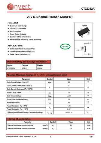
nvert CTZ2312A Suzhou Convert Semiconductor Co ., Ltd. 20V N-Channel Trench MOSFET FEATURES Super Low Gate Charge 100% EAS Guaranteed RoHS compliant Green Device Available Excellent CdV/dt effect decline Advanced high cell density Trench technology APPLICATIONS Switch Mode Power Supply (SMPS) Uninterruptible Power Supply (UPS) Power Factor Corre
fs2312.pdf
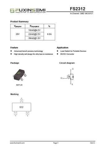
FS2312 N-Channel SMD MOSFET Product Summary V(BR)DSS RDS(on)MAX ID 18m @4.5V 20V 22m @2.5V 6.8A 39m @1.8V Feature Application Advanced trench process technology Load Switch for Portable Devices High density cell design for ultra low on-resistance DC/DC Converter Package Circuit diagram SOT-23 Marking S12 www.fuxinsemi.com Page 1 Ver2.1 FS2312 N-Channel SMD MOSFET
hss2312a.pdf
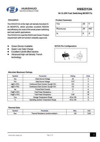
HSS2312A N-Ch 20V Fast Switching MOSFETs Description Product Summary VDS 20 V The HSS2312A is the high cell density trenched N- ch MOSFETs, which provides excellent RDSON RDS(ON),max 26 m and efficiency for most of the small power switching and load switch applications. ID 6 A The HSS2312A meet the RoHS and Green Product requirement with full function reliability approv
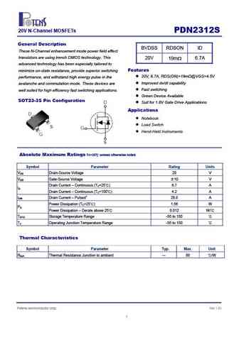
hd2312.pdf
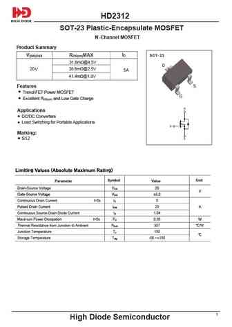
HD2312 SOT-23 Plastic-Encapsulate MOSFET N -Channel MOSFET roduct Summary P ID V(BR)DSS RDS(on)MAX SOT- 23 31.8m @4.5V D 35.6m @2.5V 20 V 5A 41.4m @1.8V S Features TrenchFET Power MOSFET G Excellent RDS(on) and Low Gate Charge Applications DC/DC Converters Load Switching for Portable Applications Marking S12 Symbol Unit Par
jmtl2312a.pdf
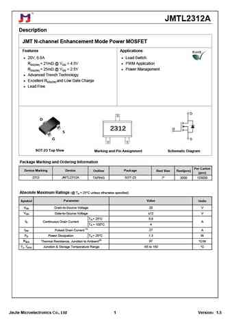
JMTL2312A Description JMT N-channel Enhancement Mode Power MOSFET Features Applications 20V, 6.8A Load Switch RDS(ON)
jmtl2312l.pdf
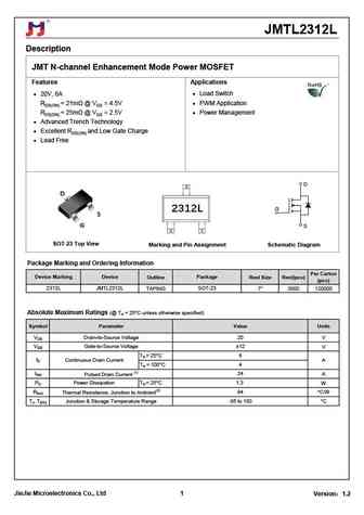
JMTL2312L Description JMT N-channel Enhancement Mode Power MOSFET Features Applications 20V, 6A Load Switch RDS(ON)
si2312.pdf
SI2312 20V N-Channel Enhancement Mode MOSFET VDS= 20V RDS(ON), Vgs@4.5V, Ids@5.0A
tf2312.pdf
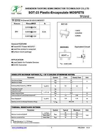
SHENZHEN TUOFENG SEMICONDUCTOR TECHNOLOGY CO.,LTD SOT-23 Plastic-Encapsulate MOSFETS TF2312 N-Channel 20-V(D-S) MOSFET TF2312 V(BR)DSS RDS(on)MAX ID SOT-23 0.031 @ 4.5V 3 1.GATE 20V 0.037 @ 2.5V 5.0A 2.SOURCE 3.DRAIN 0.047 @ 1.8V 1 2 General FEATURE TrenchFET Power MOSFET Equivalent Circuit MARKING Lead free product is acquired Surface mount package AE9TF w A
sm2312srl.pdf
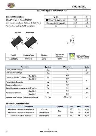
SM2312SRL 20V /6A Single N Power MOSFET B N02B N 20V /6A Single N Power MOSFET 6N02B General Description 20 V V DS 20V /6A Single N Power MOSFET 18.9 m RDS(on),TYP@VGS=10V Very low on-resistance RDS(on) @ VGS=4.5 V 42.0 m RDS(on),TYP@VGS=4.5 Pb-free lead plating; RoHS compliant 6 A ID Tape and reel Part ID Package Type Marking infomation 100% UIS Tested 100% Rg Tested SM231
si2312cds-t1-ge3.pdf
SI2312CDS-T1-GE3 www.VBsemi.tw N-Channel 20 V (D-S) MOSFET FEATURES PRODUCT SUMMARY Halogen-free According to IEC 61249-2-21 VDS (V) RDS(on) ( ) ID (A)e Qg (Typ.) Definition 0.028 at VGS = 4.5 V TrenchFET Power MOSFET 6a 100 % Rg Tested 20 0.042 at VGS = 2.5 V 6a 8.8 nC Compliant to RoHS Directive 2002/95/EC 0.050 at VGS = 1.8 V 5.6 APPLICATIONS DC/
si2312bds-t1.pdf
SI2312BDS-T1 www.VBsemi.tw N-Channel 20 V (D-S) MOSFET FEATURES PRODUCT SUMMARY Halogen-free According to IEC 61249-2-21 VDS (V) RDS(on) ( ) ID (A)e Qg (Typ.) Definition 0.028 at VGS = 4.5 V TrenchFET Power MOSFET 6a 100 % Rg Tested 20 0.042 at VGS = 2.5 V 6a 8.8 nC Compliant to RoHS Directive 2002/95/EC 0.050 at VGS = 1.8 V 5.6 APPLICATIONS DC/DC C
tsm2312cx.pdf

TSM2312CX www.VBsemi.tw N-Channel 20 V (D-S) MOSFET FEATURES PRODUCT SUMMARY Halogen-free According to IEC 61249-2-21 VDS (V) RDS(on) ( ) ID (A)e Qg (Typ.) Definition 0.028 at VGS = 4.5 V TrenchFET Power MOSFET 6a 100 % Rg Tested 20 0.042 at VGS = 2.5 V 6a 8.8 nC Compliant to RoHS Directive 2002/95/EC 0.050 at VGS = 1.8 V 5.6 APPLICATIONS DC/DC
sm2312nsa.pdf
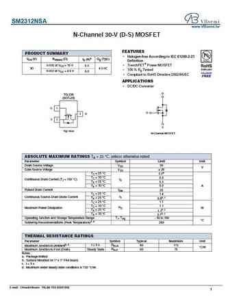
SM2312NSA www.VBsemi.tw N-Channel 30-V (D-S) MOSFET FEATURES PRODUCT SUMMARY Halogen-free According to IEC 61249-2-21 VDS (V) RDS(on) ( ) ID (A)a Qg (Typ.) Definition 0.030 at VGS = 10 V TrenchFET Power MOSFET 6.5 30 4.5 nC 100 % Rg Tested 0.033 at VGS = 4.5 V 6.0 Compliant to RoHS Directive 2002/95/EC APPLICATIONS DC/DC Converter D TO-236 (SOT-23)
cj2312.pdf
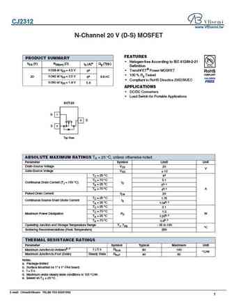
CJ2312 www.VBsemi.tw N-Channel 20 V (D-S) MOSFET FEATURES PRODUCT SUMMARY Halogen-free According to IEC 61249-2-21 VDS (V) RDS(on) ( ) ID (A)e Qg (Typ.) Definition 0.028 at VGS = 4.5 V TrenchFET Power MOSFET 6a 100 % Rg Tested 20 0.042 at VGS = 2.5 V 6a 8.8 nC Compliant to RoHS Directive 2002/95/EC 0.050 at VGS = 1.8 V 5.6 APPLICATIONS DC/DC Co
si2312ds.pdf
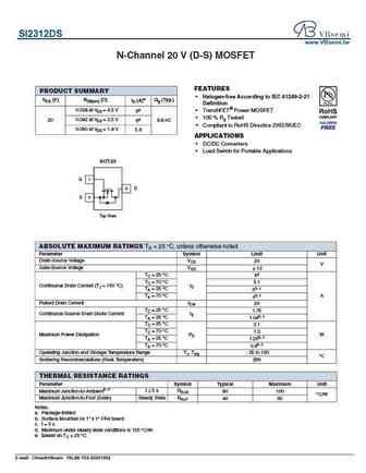
SI2312DS www.VBsemi.tw N-Channel 20 V (D-S) MOSFET FEATURES PRODUCT SUMMARY Halogen-free According to IEC 61249-2-21 VDS (V) RDS(on) ( ) ID (A)e Qg (Typ.) Definition 0.028 at VGS = 4.5 V TrenchFET Power MOSFET 6a 100 % Rg Tested 20 0.042 at VGS = 2.5 V 6a 8.8 nC Compliant to RoHS Directive 2002/95/EC 0.050 at VGS = 1.8 V 5.6 APPLICATIONS DC/DC Conve
yjl2312al.pdf
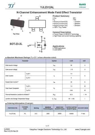
RoHS COMPLIANT YJL2312AL N-Channel Enhancement Mode Field Effect Transistor Product Summary V 20V DS I 7.6A D R ( at V =4.5V) 17mohm DS(ON) GS R ( at V =2.5V) 20mohm DS(ON) GS R ( at V =1.8V) 35mohm DS(ON) GS 100% V Tested DS General Description Trench Power LV MOSFET technology High Power and current handing capabilit
yjl2312a.pdf
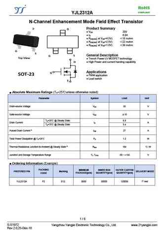
RoHS COMPLIANT YJL2312A N-Channel Enhancement Mode Field Effect Transistor Product Summary V 20V DS I 6.8A D R ( at V =4.5V) 18 mohm DS(ON) GS R ( at V =2.5V) 22 mohm DS(ON) GS R ( at V =1.8V) 39 mohm DS(ON) GS General Description Trench Power LV MOSFET technology High Power and current handing capability Applications PW
ttx2312a.pdf
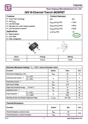
TTX2312A Wuxi Unigroup Microelectronics CO.,LTD. 20V N-Channel Trench MOSFET Features Product Summary Trench Power Technology VDS 20V Low RDS(ON) RDS(ON) (at VGS=10V)
hm2312b.pdf

HM2312B N-Channel Enhancement Mode Power MOSFET Description D The HM2312B uses advanced trench technology to provide excellent RDS(ON), low gate charge and operation with gate G voltages as low as 2.5V. This device is suitable for use as a battery protection or in other switching application. S Schematic diagram General Features VDS = 20V,ID = 4.5A RDS(ON)
hm2312.pdf
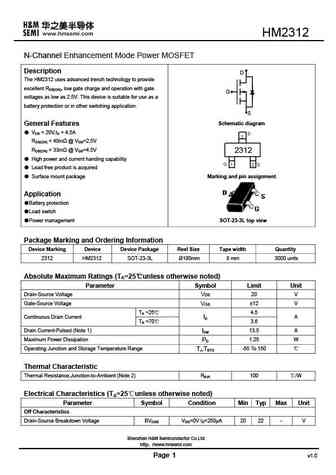
HM2312 N-Channel Enhancement Mode Power MOSFET Description D The HM2312 uses advanced trench technology to provide excellent RDS(ON), low gate charge and operation with gate G voltages as low as 2.5V. This device is suitable for use as a battery protection or in other switching application. S Schematic diagram General Features VDS = 20V,ID = 4.5A RDS(ON)
ap2312ai.pdf
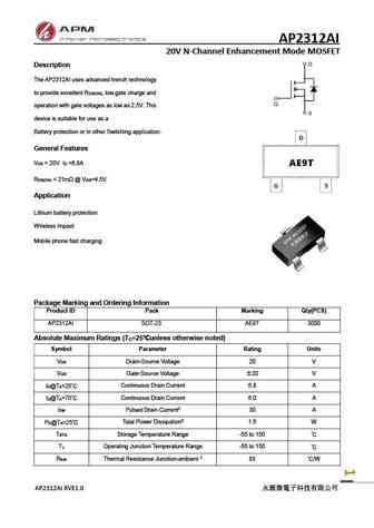
AP2312AI 20V N-Channel Enhancement Mode MOSFET Description The AP2312AI uses advanced trench technology to provide excellent R , low gate charge and DS(ON) operation with gate voltages as low as 2.5V. This device is suitable for use as a Battery protection or in other Switching application. General Features V = 20V I =6.8A DS D R
ap2312mi.pdf
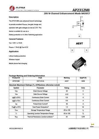
AP2312MI 20V N-Channel Enhancement Mode MOSFET Description The AP2312MI uses advanced trench technology to provide excellent R , low gate charge and DS(ON) operation with gate voltages as low as 2.5V. This device is suitable for use as a Battery protection or in other Switching application. General Features V = 20V I =6.8A DS D R
Другие MOSFET... BRFL10N65 , BRFL12N60 , BRFL12N65 , BRFL7N60 , BRFL7N65 , BRFL7N80 , BRFL8N60 , IRFB3710 , SPP20N60C3 , 06N06L , 18N10W , 2300F , 3400H , 3415A , 80N06-251 , 8680A , G01N20R .
History: TK6P60W | IXFM14N80 | TK6A80E
History: TK6P60W | IXFM14N80 | TK6A80E
🌐 : EN ES РУ

Список транзисторов
Обновления
MOSFET: AUB034N10 | AUB033N08BG | AUB026N085 | AUA062N08BG | AUA060N08AG | AUA056N08BGL | AUA039N10 | ASW80R290E | ASW65R120EFD | ASW65R110E | ASW65R095EFD | ASW65R046EFD | ASW65R041EFDA | ASW65R041E | ASW60R150E | ASW60R090EFDA
Popular searches
2sa722 | f1010e mosfet datasheet | 2sa566 | bc559 equivalent | c2075 transistor | ecg123 | 2n5551 transistor equivalent | 13009 datasheet