NVMFS3D6N10MCL. Аналоги и основные параметры
Наименование производителя: NVMFS3D6N10MCL
Тип транзистора: MOSFET
Полярность: N
Предельные значения
Pd ⓘ - Максимальная рассеиваемая мощность: 139 W
|Vds|ⓘ - Максимально допустимое напряжение сток-исток: 100 V
|Vgs|ⓘ - Максимально допустимое напряжение затвор-исток: 20 V
|Id| ⓘ - Максимально допустимый постоянный ток стока: 132 A
Tj ⓘ - Максимальная температура канала: 175 °C
Электрические характеристики
tr ⓘ - Время нарастания: 7 ns
Cossⓘ - Выходная емкость: 1808 pf
RDSonⓘ - Сопротивление сток-исток открытого транзистора: 0.0036 Ohm
Тип корпуса: DFN5
Аналог (замена) для NVMFS3D6N10MCL
- подборⓘ MOSFET транзистора по параметрам
NVMFS3D6N10MCL даташит
nvmfs3d6n10mcl.pdf
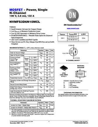
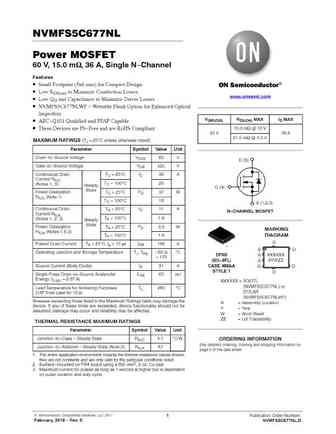
MOSFET - Power, Single N-Channel 100 V, 3.6 mW, 132 A NVMFS3D6N10MCL Features www.onsemi.com Small Footprint (5x6 mm) for Compact Design Low RDS(on) to Minimize Conduction Losses Low QG and Capacitance to Minimize Driver Losses V(BR)DSS RDS(ON) MAX ID MAX NVMFWS3D6N10MCL - Wettable Flank Option for Enhanced 3.6 mW @ 10 V Optical Inspection 100 V 132 A 5.8 mW @ 4.5
nvmfs6h858nl.pdf
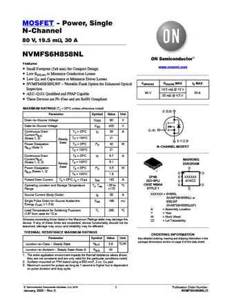
MOSFET - Power, Single N-Channel 80 V, 19.5 mW, 30 A NVMFS6H858NL Features www.onsemi.com Small Footprint (5x6 mm) for Compact Design Low RDS(on) to Minimize Conduction Losses Low QG and Capacitance to Minimize Driver Losses V(BR)DSS RDS(ON) MAX ID MAX NVMFS6H858NLWF - Wettable Flank Option for Enhanced Optical Inspection 19.5 mW @ 10 V 80 V 30 A AEC-Q101 Quali
nvmfs5c450nl.pdf

NVMFS5C450NL Power MOSFET 40 V, 2.8 mW, 110 A, Single N-Channel Features Small Footprint (5x6 mm) for Compact Design Low RDS(on) to Minimize Conduction Losses www.onsemi.com Low QG and Capacitance to Minimize Driver Losses NVMFS5C450NLWF - Wettable Flank Option for Enhanced Optical Inspection V(BR)DSS RDS(ON) MAX ID MAX AEC-Q101 Qualified and PPAP Capable 2.8 mW
nvmfs5c404nl.pdf
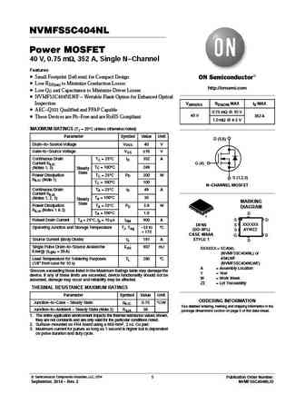
NVMFS5C404NL Power MOSFET 40 V, 0.75 mW, 352 A, Single N-Channel Features Small Footprint (5x6 mm) for Compact Design Low RDS(on) to Minimize Conduction Losses http //onsemi.com Low QG and Capacitance to Minimize Driver Losses NVMFS5C404NLWF - Wettable Flank Option for Enhanced Optical Inspection V(BR)DSS RDS(ON) MAX ID MAX AEC-Q101 Qualified and PPAP Capable 0.7
nvmfs6h824n.pdf

MOSFET - Power, Single N-Channel 80 V, 4.5 mW, 107 A NVMFS6H824N Features www.onsemi.com Small Footprint (5x6 mm) for Compact Design Low RDS(on) to Minimize Conduction Losses Low QG and Capacitance to Minimize Driver Losses NVMFS6H824NWF - Wettable Flank Option for Enhanced Optical V(BR)DSS RDS(ON) MAX ID MAX Inspection 80 V 4.5 mW @ 10 V 107 A AEC-Q101 Qualifie
nvmfs4c302n.pdf
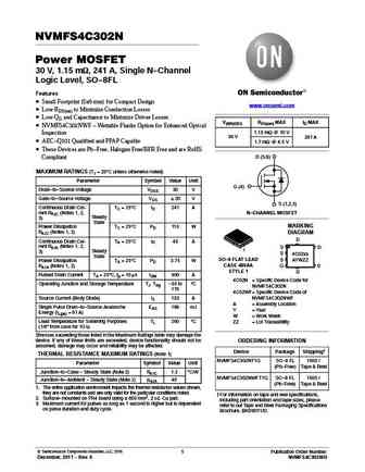
NVMFS4C302N Power MOSFET 30 V, 1.15 mW, 241 A, Single N-Channel Logic Level, SO-8FL Features Small Footprint (5x6 mm) for Compact Design www.onsemi.com Low RDS(on) to Minimize Conduction Losses Low QG and Capacitance to Minimize Driver Losses V(BR)DSS RDS(on) MAX ID MAX NVMFS4C302NWF - Wettable Flanks Option for Enhanced Optical 1.15 mW @ 10 V Inspection 30 V 241 A
nvmfs5c460n.pdf
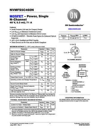
NVMFS5C460N MOSFET Power, Single N-Channel 40 V, 5.3 mW, 71 A Features www.onsemi.com Small Footprint (5x6 mm) for Compact Design Low RDS(on) to Minimize Conduction Losses Low QG and Capacitance to Minimize Driver Losses V(BR)DSS RDS(ON) MAX ID MAX NVMFS5C460NWF - Wettable Flank Option for Enhanced Optical Inspection 40 V 5.3 mW @ 10 V 71 A AEC-Q101 Qualified
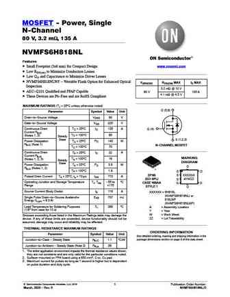
nvmfs6h818n.pdf
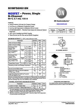
NVMFS6H818N MOSFET Power, Single N-Channel 80 V, 3.7 mW, 123 A Features www.onsemi.com Small Footprint (5x6 mm) for Compact Design Low RDS(on) to Minimize Conduction Losses Low QG and Capacitance to Minimize Driver Losses V(BR)DSS RDS(ON) MAX ID MAX NVMFS6H818NWF - Wettable Flank Option for Enhanced Optical Inspection 80 V 3.7 mW @ 10 V 123 A AEC-Q101 Qualif
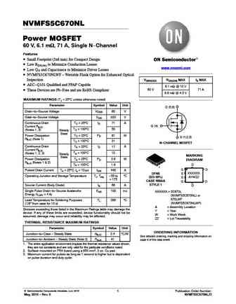
nvmfs5c670n.pdf
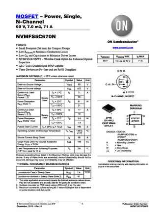
MOSFET Power, Single, N-Channel 60 V, 7.0 mW, 71 A NVMFS5C670N Features www.onsemi.com Small Footprint (5x6 mm) for Compact Design Low RDS(on) to Minimize Conduction Losses Low QG and Capacitance to Minimize Driver Losses V(BR)DSS RDS(ON) MAX ID MAX NVMFS5C670NWF - Wettable Flank Option for Enhanced Optical 60 V 7.0 mW @ 10 V 71 A Inspection AEC-Q101 Qualifi
nvmfs5832nl.pdf
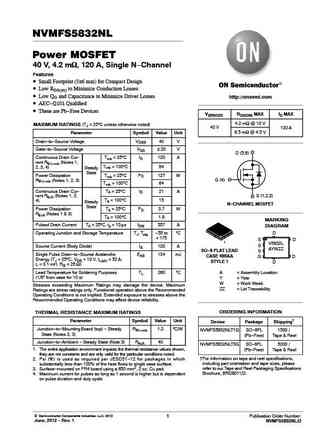
NVMFS5832NL Power MOSFET 40 V, 4.2 mW, 120 A, Single N-Channel Features Small Footprint (5x6 mm) for Compact Design Low RDS(on) to Minimize Conduction Losses Low QG and Capacitance to Minimize Driver Losses http //onsemi.com AEC-Q101 Qualified These are Pb-Free Devices V(BR)DSS RDS(ON) MAX ID MAX 4.2 mW @ 10 V MAXIMUM RATINGS (TJ = 25 C unless otherwise noted)
nvmfs5c604nl.pdf
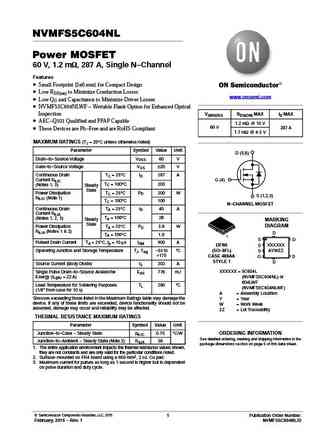
NVMFS5C604NL Power MOSFET 60 V, 1.2 mW, 287 A, Single N-Channel Features Small Footprint (5x6 mm) for Compact Design Low RDS(on) to Minimize Conduction Losses www.onsemi.com Low QG and Capacitance to Minimize Driver Losses NVMFS5C604NLWF - Wettable Flank Option for Enhanced Optical Inspection V(BR)DSS RDS(ON) MAX ID MAX AEC-Q101 Qualified and PPAP Capable 1.2 mW
nvmfs6h848n.pdf

MOSFET - Power, Single N-Channel 80 V, 9.4 mW, 64 A NVMFS6H848N Features www.onsemi.com Small Footprint (5x6 mm) for Compact Design Low RDS(on) to Minimize Conduction Losses Low QG and Capacitance to Minimize Driver Losses NVMFS6H848NWF - Wettable Flank Option for Enhanced Optical V(BR)DSS RDS(ON) MAX ID MAX Inspection 80 V 9.4 mW @ 10 V 64 A AEC-Q101 Qualified
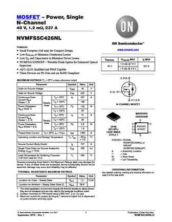
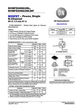
nvmfs5h663nl nvmfs5h663nlwf.pdf

NVMFS5H663NL, NVMFS5H663NLWF MOSFET Power, Single N-Channel 60 V, 7.2 mW, 67 A www.onsemi.com NVMFS5H663NLWF - Wettable Flank Option for Enhanced Optical Inspection. V(BR)DSS RDS(ON) MAX ID MAX Features Small Footprint (5x6 mm) for Compact Design 7.2 mW @ 10 V 60 V 67 A Low RDS(on) to Minimize Conduction Losses 10 mW @ 4.5 V Low QG and Capacitance to Minimize Dri
nvmfs5c680nl.pdf
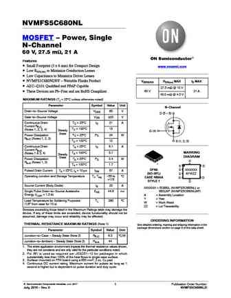
NVMFS5C680NL MOSFET Power, Single N-Channel 60 V, 27.5 mW, 21 A Features Small Footprint (5 x 6 mm) for Compact Design www.onsemi.com Low RDS(on) to Minimize Conduction Losses Low Capacitance to Minimize Driver Losses NVMFS5C680NLWF - Wettable Flanks Product V(BR)DSS RDS(on) MAX ID MAX AEC-Q101 Qualified and PPAP Capable 27.5 mW @ 10 V 60 V 21 A These D
nvmfs6b14nl.pdf
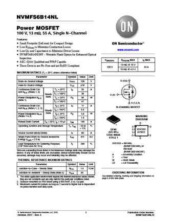
NVMFS6B14NL Power MOSFET 100 V, 13 mW, 55 A, Single N-Channel Features Small Footprint (5x6 mm) for Compact Design Low RDS(on) to Minimize Conduction Losses www.onsemi.com Low QG and Capacitance to Minimize Driver Losses NVMFS6B14NLWF - Wettable Flank Option for Enhanced Optical Inspection V(BR)DSS RDS(ON) MAX ID MAX AEC-Q101 Qualified and PPAP Capable 13 mW @ 10
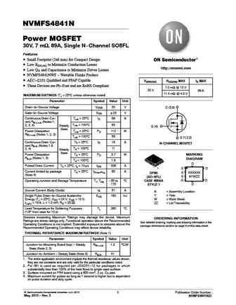
nvmfs4841n-d.pdf
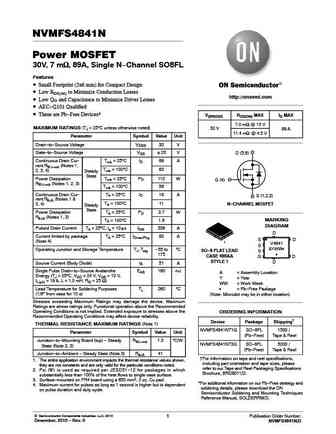
NVMFS4841N Power MOSFET 30V, 7 mW, 89A, Single N-Channel SO8FL Features Small Footprint (5x6 mm) for Compact Design Low RDS(on) to Minimize Conduction Losses http //onsemi.com Low QG and Capacitance to Minimize Driver Losses AEC-Q101 Qualified These are Pb-Free Devices* V(BR)DSS RDS(ON) MAX ID MAX 7.0 mW @ 10 V MAXIMUM RATINGS (TJ = 25 C unless otherwise noted)
ntmfs5834nl nvmfs5834nl.pdf
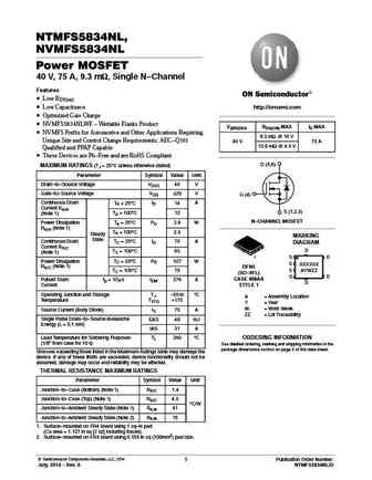
NTMFS5834NL, NVMFS5834NL Power MOSFET 40 V, 75 A, 9.3 mW, Single N-Channel Features Low RDS(on) Low Capacitance http //onsemi.com Optimized Gate Charge NVMFS5834NLWF - Wettable Flanks Product V(BR)DSS RDS(ON) MAX ID MAX NVMFS Prefix for Automotive and Other Applications Requiring 9.3 mW @ 10 V Unique Site and Control Change Requirements; AEC-Q101 40 V 75 A 13.6
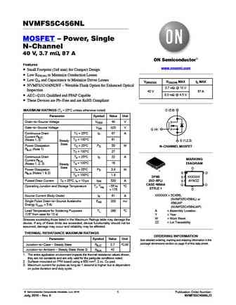
nvmfs5c460nl.pdf

NVMFS5C460NL MOSFET Power, Single N-Channel 40 V, 4.5 mW, 78 A Features www.onsemi.com Small Footprint (5x6 mm) for Compact Design Low RDS(on) to Minimize Conduction Losses Low QG and Capacitance to Minimize Driver Losses V(BR)DSS RDS(ON) MAX ID MAX NVMFS5C460NLWF - Wettable Flank Option for Enhanced Optical 4.5 mW @ 10 V Inspection 40 V 78 A 7.2 mW @ 4.5 V
nvmfs5c410nl.pdf
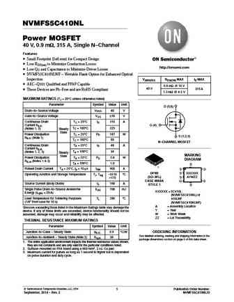
NVMFS5C410NL Power MOSFET 40 V, 0.9 mW, 315 A, Single N-Channel Features Small Footprint (5x6 mm) for Compact Design Low RDS(on) to Minimize Conduction Losses http //onsemi.com Low QG and Capacitance to Minimize Driver Losses NVMFS5C410NLWF - Wettable Flank Option for Enhanced Optical Inspection V(BR)DSS RDS(ON) MAX ID MAX AEC-Q101 Qualified and PPAP Capable 0.9
nvmfs015n10mcl.pdf
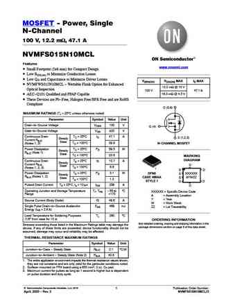
MOSFET - Power, Single N-Channel 100 V, 12.2 mW, 47.1 A NVMFS015N10MCL Features www.onsemi.com Small Footprint (5x6 mm) for Compact Design Low RDS(on) to Minimize Conduction Losses Low QG and Capacitance to Minimize Driver Losses V(BR)DSS RDS(ON) MAX ID MAX NVMFWS015N10MCL - Wettable Flank Option for Enhanced 12.2 mW @ 10 V Optical Inspection 100 V 47.1 A 18.3 mW @
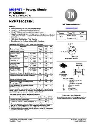
nvmfs5c673n.pdf
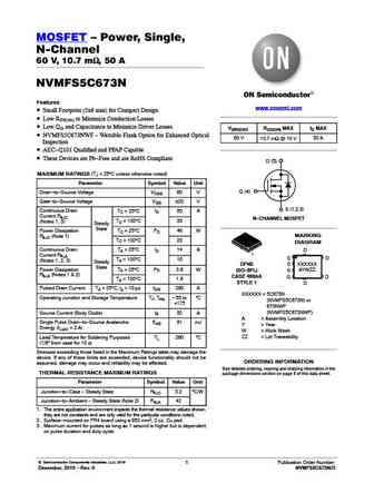
MOSFET Power, Single, N-Channel 60 V, 10.7 mW, 50 A NVMFS5C673N Features www.onsemi.com Small Footprint (5x6 mm) for Compact Design Low RDS(on) to Minimize Conduction Losses Low QG and Capacitance to Minimize Driver Losses V(BR)DSS RDS(ON) MAX ID MAX NVMFS5C673NWF - Wettable Flank Option for Enhanced Optical 60 V 10.7 mW @ 10 V 50 A Inspection AEC-Q101 Quali
nvmfs6h801nl.pdf

MOSFET - Power, Single N-Channel 80 V, 2.7 mW, 160 A NVMFS6H801NL Features www.onsemi.com Small Footprint (5x6 mm) for Compact Design Low RDS(on) to Minimize Conduction Losses Low QG and Capacitance to Minimize Driver Losses NVMFS6H801NLWF - Wettable Flank Option for Enhanced Optical V(BR)DSS RDS(ON) MAX ID MAX Inspection 2.7 mW @ 10 V AEC-Q101 Qualified and PPA
nvmfs6h852n.pdf
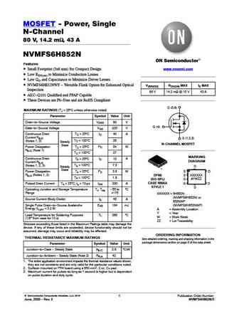
MOSFET - Power, Single N-Channel 80 V, 14.2 mW, 43 A NVMFS6H852N Features www.onsemi.com Small Footprint (5x6 mm) for Compact Design Low RDS(on) to Minimize Conduction Losses Low QG and Capacitance to Minimize Driver Losses NVMFS6H852NWF - Wettable Flank Option for Enhanced Optical V(BR)DSS RDS(ON) MAX ID MAX Inspection 80 V 14.2 mW @ 10 V 43 A AEC-Q101 Qualifie
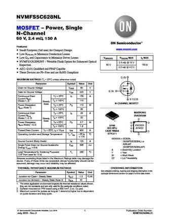
nvmfs5c628n.pdf
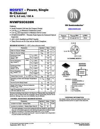
MOSFET - Power, Single N-Channel 60 V, 3.0 mW, 150 A NVMFS5C628N Features Small Footprint (5x6 mm) for Compact Design www.onsemi.com Low RDS(on) to Minimize Conduction Losses Low QG and Capacitance to Minimize Driver Losses NVMFS5C628NWF - Wettable Flank Option for Enhanced Optical V(BR)DSS RDS(ON) MAX ID MAX Inspection 60 V 3.0 mW @ 10 V 150 A AEC-Q101 Qualifie
nvmfs5c638nl.pdf
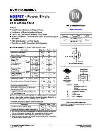
NVMFS5C638NL MOSFET Power, Single N-Channel 60 V, 3.0 mW, 133 A Features www.onsemi.com Small Footprint (5x6 mm) for Compact Design Low RDS(on) to Minimize Conduction Losses Low QG and Capacitance to Minimize Driver Losses V(BR)DSS RDS(ON) MAX ID MAX NVMFS5C638NLWF - Wettable Flank Option for Enhanced Optical 3.0 mW @ 10 V Inspection 60 V 133 A AEC-Q101 Qua
nvmfs6h864n.pdf
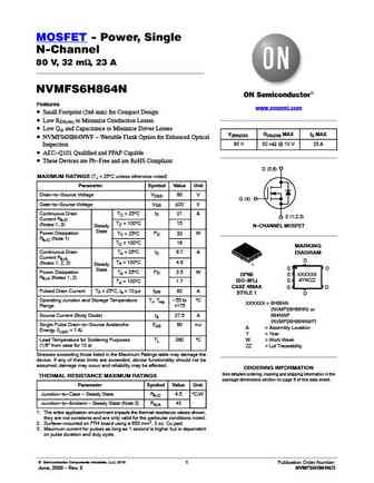
MOSFET - Power, Single N-Channel 80 V, 32 mW, 23 A NVMFS6H864N Features www.onsemi.com Small Footprint (5x6 mm) for Compact Design Low RDS(on) to Minimize Conduction Losses Low QG and Capacitance to Minimize Driver Losses V(BR)DSS RDS(ON) MAX ID MAX NVMFS6H864NWF - Wettable Flank Option for Enhanced Optical 80 V 32 mW @ 10 V 23 A Inspection AEC-Q101 Qualified an
nvmfs5833n.pdf
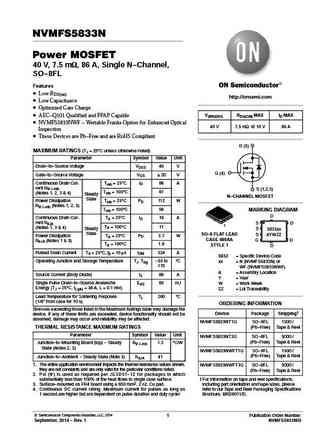
NVMFS5833N Power MOSFET 40 V, 7.5 mW, 86 A, Single N-Channel, SO-8FL Features Low RDS(on) http //onsemi.com Low Capacitance Optimized Gate Charge V(BR)DSS RDS(ON) MAX ID MAX AEC-Q101 Qualified and PPAP Capable NVMFS5833NWF - Wettable Franks Option for Enhanced Optical 40 V 7.5 mW @ 10 V 86 A Inspection These Devices are Pb-Free and are RoHS Compliant D (5)
nvmfs6d1n08h.pdf
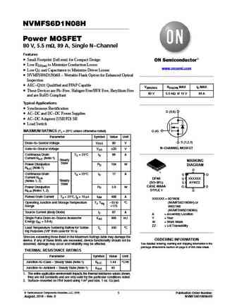
NVMFS6D1N08H Power MOSFET 80 V, 5.5 mW, 89 A, Single N-Channel Features Small Footprint (5x6 mm) for Compact Design Low RDS(on) to Minimize Conduction Losses www.onsemi.com Low QG and Capacitance to Minimize Driver Losses NVMFSW6D1N08H - Wettable Flank Option for Enhanced Optical Inspection AEC-Q101 Qualified and PPAP Capable V(BR)DSS RDS(ON) MAX ID MAX These
nvmfs5h600nl.pdf
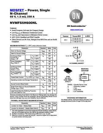
MOSFET Power, Single N-Channel 60 V, 1.3 mW, 250 A NVMFS5H600NL Features www.onsemi.com Small Footprint (5x6 mm) for Compact Design Low RDS(on) to Minimize Conduction Losses Low QG and Capacitance to Minimize Driver Losses V(BR)DSS RDS(ON) MAX ID MAX AEC-Q101 Qualified and PPAP Capable 1.3 mW @ 10 V These Devices are Pb-Free, Halogen Free/BFR Free and are RoH
nvmfs5c468n.pdf
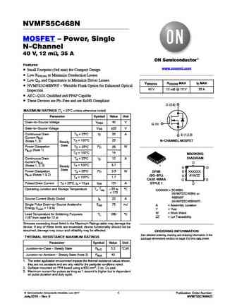
NVMFS5C468N MOSFET Power, Single N-Channel 40 V, 12 mW, 35 A Features www.onsemi.com Small Footprint (5x6 mm) for Compact Design Low RDS(on) to Minimize Conduction Losses Low QG and Capacitance to Minimize Driver Losses V(BR)DSS RDS(ON) MAX ID MAX NVMFS5C468NWF - Wettable Flank Option for Enhanced Optical 40 V 12 mW @ 10 V 35 A Inspection AEC-Q101 Qualified
nvmfs6h818nl.pdf
MOSFET - Power, Single N-Channel 80 V, 3.2 mW, 135 A NVMFS6H818NL Features www.onsemi.com Small Footprint (5x6 mm) for Compact Design Low RDS(on) to Minimize Conduction Losses Low QG and Capacitance to Minimize Driver Losses NVMFS6H818NLWF - Wettable Flank Option for Enhanced Optical V(BR)DSS RDS(ON) MAX ID MAX Inspection 3.2 mW @ 10 V AEC-Q101 Qualified and PPA
nvmfs6h801n.pdf

MOSFET Power, Single, N-Channel 80 V, 2.8 mW, 157 A NVMFS6H801N Features www.onsemi.com Small Footprint (5x6 mm) for Compact Design Low RDS(on) to Minimize Conduction Losses Low QG and Capacitance to Minimize Driver Losses V(BR)DSS RDS(ON) MAX ID MAX NVMFS6H801NWF - Wettable Flank Option for Enhanced Optical Inspection 80 V 2.8 mW @ 10 V 157 A AEC-Q101 Quali
nvmfs5c404n.pdf
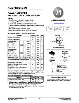
NVMFS5C404N Power MOSFET 40 V, 0.7 mW, 378 A, Single N-Channel Features Small Footprint (5x6 mm) for Compact Design Low RDS(on) to Minimize Conduction Losses www.onsemi.com Low QG and Capacitance to Minimize Driver Losses NVMFS5C404NWF - Wettable Flank Option for Enhanced Optical Inspection V(BR)DSS RDS(ON) MAX ID MAX AEC-Q101 Qualified and PPAP Capable 40 V 0.7
nvmfs5c682nl.pdf

NVMFS5C682NL MOSFET Power, Single N-Channel 60 V, 21 mW, 25 A Features www.onsemi.com Small Footprint (5x6 mm) for Compact Design Low RDS(on) to Minimize Conduction Losses Low QG and Capacitance to Minimize Driver Losses V(BR)DSS RDS(ON) MAX ID MAX NVMFS5C682NLWF - Wettable Flank Option for Enhanced Optical 21 mW @ 10 V 60 V 25 A Inspection 31.5 mW @ 4.5 V
nvmfs4841n.pdf
NVMFS4841N Power MOSFET 30V, 7 mW, 89A, Single N-Channel SO8FL Features Small Footprint (5x6 mm) for Compact Design Low RDS(on) to Minimize Conduction Losses http //onsemi.com Low QG and Capacitance to Minimize Driver Losses NVMFS4841NWF - Wettable Flanks Product AEC-Q101 Qualified and PPAP Capable V(BR)DSS RDS(ON) MAX ID MAX These Devices are Pb-Free and are
nvmfs5c673nl.pdf
MOSFET Power, Single N-Channel 60 V, 9.2 mW, 50 A NVMFS5C673NL Features www.onsemi.com Small Footprint (5x6 mm) for Compact Design Low RDS(on) to Minimize Conduction Losses Low QG and Capacitance to Minimize Driver Losses V(BR)DSS RDS(ON) MAX ID MAX NVMFS5C673NLWF - Wettable Flank Option for Enhanced Optical 9.2 mW @ 10 V 60 V 50 A Inspection 13 mW @ 4.5 V
nvmfs5a160plz.pdf
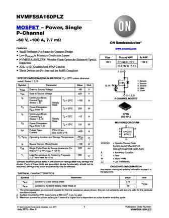
NVMFS5A160PLZ MOSFET Power, Single P-Channel -60 V, -100 A, 7.7 mW Features www.onsemi.com Small Footprint (5 x 6 mm) for Compact Design Low RDS(on) to Minimize Conduction Losses VDSS RDS(ON) MAX ID MAX NVMFS5A160PLZWF Wettable Flank Option for Enhanced Optical -60 V 7.7 mW @ -10 V -100 A Inspection 10.5 mW @ -4.5 V AEC-Q101 Qualified and PPAP Capable Thes
nvmfs5830nl.pdf
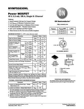
NVMFS5830NL Power MOSFET 40 V, 2.3 mW, 185 A, Single N-Channel Features Small Footprint (5x6 mm) for Compact Design Low RDS(on) to Minimize Conduction Losses http //onsemi.com Low QG and Capacitance to Minimize Driver Losses NVMFS5830NLWF - Wettable Flanks Product V(BR)DSS RDS(ON) MAX ID MAX AEC-Q101 Qualified and PPAP Capable These Devices are Pb-Free and are
nvmfs6b75nl.pdf
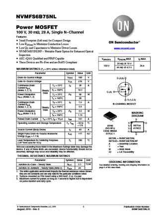
NVMFS6B75NL Power MOSFET 100 V, 30 mW, 28 A, Single N-Channel Features Small Footprint (5x6 mm) for Compact Design Low RDS(on) to Minimize Conduction Losses Low QG and Capacitance to Minimize Driver Losses www.onsemi.com NVMFS6B75NLWF - Wettable Flank Option for Enhanced Optical Inspection AEC-Q101 Qualified and PPAP Capable V(BR)DSS RDS(ON) MAX ID MAX These
ntmfs5844nl nvmfs5844nl.pdf
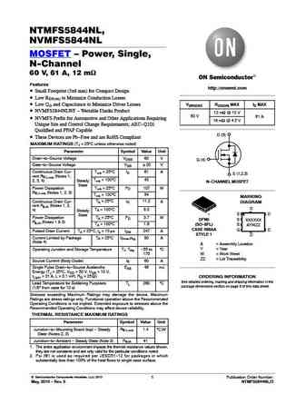
NTMFS5844NL, NVMFS5844NL MOSFET Power, Single, N-Channel 60 V, 61 A, 12 mW Features http //onsemi.com Small Footprint (5x6 mm) for Compact Design Low RDS(on) to Minimize Conduction Losses Low QG and Capacitance to Minimize Driver Losses V(BR)DSS RDS(ON) MAX ID MAX NVMFS5844NLWF - Wettable Flanks Product 12 mW @ 10 V 60 V 61 A NVMFS Prefix for Automotive and
nvmfs5c612nl.pdf

NVMFS5C612NL Power MOSFET 60 V, 1.5 mW, 235 A, Single N-Channel Features Small Footprint (5x6 mm) for Compact Design Low RDS(on) to Minimize Conduction Losses www.onsemi.com Low QG and Capacitance to Minimize Driver Losses NVMFS5C612NLWF - Wettable Flank Option for Enhanced Optical Inspection V(BR)DSS RDS(ON) MAX ID MAX AEC-Q101 Qualified and PPAP Capable 1.5 mW
nvmfs5c426nl.pdf
MOSFET Power, Single N-Channel 40 V, 1.2 mW, 237 A NVMFS5C426NL Features www.onsemi.com Small Footprint (5x6 mm) for Compact Design Low RDS(on) to Minimize Conduction Losses Low QG and Capacitance to Minimize Driver Losses V(BR)DSS RDS(ON) MAX ID MAX NVMFS5C426NLWF - Wettable Flank Option for Enhanced Optical 1.2 mW @ 10 V Inspection 40 V 237 A 1.8 mW @ 4.5 V
nvmfs5a140plz.pdf
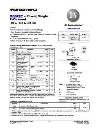
NVMFS5A140PLZ MOSFET Power, Single P-Channel -40 V, -140 A, 4.2 mW Features www.onsemi.com Small Footprint (5 x 6 mm) for Compact Design Low RDS(on) to Minimize Conduction Losses NVMFS5A140PLZWF Wettable Flank Option for Enhanced Optical VDSS RDS(ON) MAX ID MAX Inspection -40 V 4.2 mW @ -10 V -140 A AEC-Q101 Qualified and PPAP Capable 7.2 mW @ -4.5 V These
nvmfs5885nl.pdf
NVMFS5885NL Power MOSFET 60 V, 15 mW, 39 A, Single N-Channel Features Small Footprint (5x6 mm) for Compact Design Low RDS(on) to Minimize Conduction Losses http //onsemi.com Low Capacitance to Minimize Driver Losses NVMFS5885NLWF - Wettable Flanks Product V(BR)DSS RDS(ON) MAX ID MAX AEC-Q101 Qualified and PPAP Capable These Devices are Pb-Free and are RoHS Com
nvmfs5c612n.pdf
NVMFS5C612N Power MOSFET Single N-Channel, 60 V, 1.65 mW, 225 A Features Small Footprint (5x6 mm) for Compact Design Low RDS(on) to Minimize Conduction Losses www.onsemi.com Low QG and Capacitance to Minimize Driver Losses NVMFS5C612NWF - Wettable Flank Option for Enhanced Optical Inspection V(BR)DSS RDS(ON) MAX ID MAX AEC-Q101 Qualified and PPAP Capable 60 V 1.6
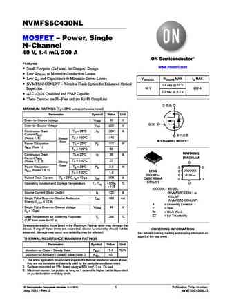
nvmfs5c430n.pdf
NVMFS5C430N MOSFET Power, Single N-Channel 40 V, 1.7 mW, 185 A Features www.onsemi.com Small Footprint (5x6 mm) for Compact Design Low RDS(on) to Minimize Conduction Losses Low QG and Capacitance to Minimize Driver Losses V(BR)DSS RDS(ON) MAX ID MAX NVMFS5C430NWF - Wettable Flank Option for Enhanced Optical 40 V 1.7 mW @ 10 V 185 A Inspection AEC-Q101 Qualif
nvmfs6h800nl.pdf
NVMFS6H800NL Power MOSFET Single N-Channel, 80 V, 1.9 mW, 224 A Features Small Footprint (5x6 mm) for Compact Design Low RDS(on) to Minimize Conduction Losses www.onsemi.com Low QG and Capacitance to Minimize Driver Losses NVMFS6H800NLWF - Wettable Flank Option for Enhanced Optical Inspection V(BR)DSS RDS(ON) MAX ID MAX AEC-Q101 Qualified and PPAP Capable The
nvmfs6h836nl.pdf

MOSFET - Power, Single N-Channel 80 V, 6.2 mW, 77 A NVMFS6H836NL Features www.onsemi.com Small Footprint (5x6 mm) for Compact Design Low RDS(on) to Minimize Conduction Losses Low QG and Capacitance to Minimize Driver Losses V(BR)DSS RDS(ON) MAX ID MAX NVMFS6H836NLWF - Wettable Flank Option for Enhanced Optical Inspection 6.2 mW @ 10 V 80 V 77 A AEC-Q101 Qualif
nvmfs6h836n.pdf

MOSFET - Power, Single N-Channel 80 V, 6.7 mW, 80 A NVMFS6H836N Features www.onsemi.com Small Footprint (5x6 mm) for Compact Design Low RDS(on) to Minimize Conduction Losses Low QG and Capacitance to Minimize Driver Losses V(BR)DSS RDS(ON) MAX ID MAX NVMFS6H836NWF - Wettable Flank Option for Enhanced Optical Inspection 80 V 6.7 mW @ 10 V 80 A AEC-Q101 Qualified
nvmfs020n06c.pdf

MOSFET- Power, Single N-Channel, SO-8FL 60 V, 19.6 mW, 28 A NVMFS020N06C Features Small Footprint (5x6 mm) for Compact Design www.onsemi.com Low RDS(on) to Minimize Conduction Losses Low QG and Capacitance to Minimize Driver Losses NVMFWS020N06C - Wettable Flank Option for Enhanced Optical V(BR)DSS RDS(ON) MAX ID MAX Inspection 60 V 19.6 mW @ 10 V 28 A AEC-Q101
nvmfs5c406nl.pdf
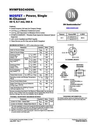
NVMFS5C406NL MOSFET Power, Single N-Channel 40 V, 0.7 mW, 362 A Features www.onsemi.com Small Footprint (5x6 mm) for Compact Design Low RDS(on) to Minimize Conduction Losses Low QG and Capacitance to Minimize Driver Losses V(BR)DSS RDS(ON) MAX ID MAX NVMFS5C406NLWF - Wettable Flank Option for Enhanced Optical 0.7 mW @ 10 V Inspection 40 V 362 A AEC-Q101 Qua
nvmfs016n06c.pdf
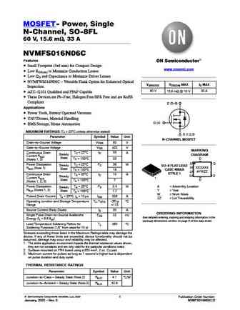
MOSFET- Power, Single N-Channel, SO-8FL 60 V, 15.6 mW, 33 A NVMFS016N06C Features Small Footprint (5x6 mm) for Compact Design www.onsemi.com Low RDS(on) to Minimize Conduction Losses Low QG and Capacitance to Minimize Driver Losses NVMFWS016N06C - Wettable Flank Option for Enhanced Optical V(BR)DSS RDS(ON) MAX ID MAX Inspection 60 V 15.6 mW @ 10 V 33 A AEC-Q101
nvmfs4c05n.pdf
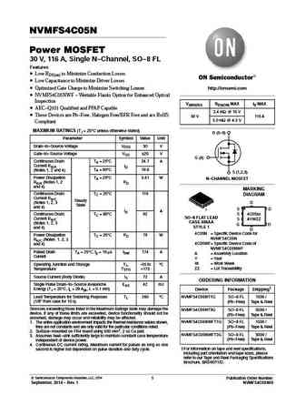
NVMFS4C05N Power MOSFET 30 V, 116 A, Single N-Channel, SO-8 FL Features Low RDS(on) to Minimize Conduction Losses Low Capacitance to Minimize Driver Losses Optimized Gate Charge to Minimize Switching Losses http //onsemi.com NVMFS4C05NWF - Wettable Flanks Option for Enhanced Optical Inspection V(BR)DSS RDS(ON) MAX ID MAX AEC-Q101 Qualified and PPAP Capable 3.4 mW
nvmfs5c423nl.pdf
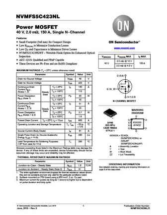
NVMFS5C423NL Power MOSFET 40 V, 2.0 mW, 150 A, Single N-Channel Features Small Footprint (5x6 mm) for Compact Design Low RDS(on) to Minimize Conduction Losses www.onsemi.com Low QG and Capacitance to Minimize Driver Losses NVMFS5C423NLWF - Wettable Flank Option for Enhanced Optical Inspection V(BR)DSS RDS(ON) MAX ID MAX AEC-Q101 Qualified and PPAP Capable 2.0 mW
nvmfs5c468nl.pdf

NVMFS5C468NL MOSFET Power, Single N-Channel 40 V, 10.3 mW, 37 A Features www.onsemi.com Small Footprint (5x6 mm) for Compact Design Low RDS(on) to Minimize Conduction Losses Low QG and Capacitance to Minimize Driver Losses V(BR)DSS RDS(ON) MAX ID MAX NVMFS5C468NLWF - Wettable Flank Option for Enhanced Optical 10.3 mW @ 10 V Inspection 40 V 37 A 17.6 mW @ 4.5 V
nvmfs5c466n.pdf

NVMFS5C466N MOSFET Power, Single N-Channel 40 V, 8.1 mW, 49 A Features www.onsemi.com Small Footprint (5x6 mm) for Compact Design Low RDS(on) to Minimize Conduction Losses Low QG and Capacitance to Minimize Driver Losses V(BR)DSS RDS(ON) MAX ID MAX NVMFS5C466NWF - Wettable Flank Option for Enhanced Optical 40 V 8.1 mW @ 10 V 49 A Inspection AEC-Q101 Qualifie
nvmfs5h663nl.pdf
NVMFS5H663NL, NVMFS5H663NLWF MOSFET Power, Single N-Channel 60 V, 7.2 mW, 67 A www.onsemi.com NVMFS5H663NLWF - Wettable Flank Option for Enhanced Optical Inspection. V(BR)DSS RDS(ON) MAX ID MAX Features Small Footprint (5x6 mm) for Compact Design 7.2 mW @ 10 V 60 V 67 A Low RDS(on) to Minimize Conduction Losses 10 mW @ 4.5 V Low QG and Capacitance to Minimize Dri
nvmfs5c442n.pdf
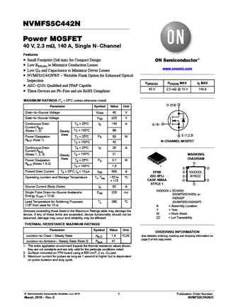
NVMFS5C442N Power MOSFET 40 V, 2.3 mW, 140 A, Single N-Channel Features Small Footprint (5x6 mm) for Compact Design Low RDS(on) to Minimize Conduction Losses www.onsemi.com Low QG and Capacitance to Minimize Driver Losses NVMFS5C442NWF - Wettable Flank Option for Enhanced Optical Inspection V(BR)DSS RDS(ON) MAX ID MAX AEC-Q101 Qualified and PPAP Capable 40 V 2.3
nvmfs5c670nl.pdf
NVMFS5C670NL Power MOSFET 60 V, 6.1 mW, 71 A, Single N-Channel Features Small Footprint (5x6 mm) for Compact Design Low RDS(on) to Minimize Conduction Losses www.onsemi.com Low QG and Capacitance to Minimize Driver Losses NVMFS5C670NLWF - Wettable Flank Option for Enhanced Optical Inspection V(BR)DSS RDS(ON) MAX ID MAX AEC-Q101 Qualified and PPAP Capable 6.1 mW @
nvmfs6h824nl.pdf

MOSFET - Power, Single N-Channel 80 V, 4 mW, 110 A NVMFS6H824NL Features www.onsemi.com Small Footprint (5x6 mm) for Compact Design Low RDS(on) to Minimize Conduction Losses Low QG and Capacitance to Minimize Driver Losses V(BR)DSS RDS(ON) MAX ID MAX NVMFS6H824NLWF - Wettable Flank Option for Enhanced Optical Inspection 4 mW @ 10 V 80 V 110 A AEC-Q101 Qualified
nvmfs4c03n.pdf
NVMFS4C03N Power MOSFET 30 V, 2.1 mW, 143 A, Single N-Channel Logic Level, SO-8FL Features http //onsemi.com Small Footprint (5x6 mm) for Compact Design Low RDS(on) to Minimize Conduction Losses V(BR)DSS RDS(on) MAX ID MAX Low QG and Capacitance to Minimize Driver Losses 2.1 mW @ 10 V 30 V NVMFS4C03NWF - Wettable Flanks Option for Enhanced Optical 143 A 2.8 mW @ 4.5
nvmfs5c645nl.pdf
NVMFS5C645NL Power MOSFET 60 V, 4.0 mW, 100 A, Single N-Channel Features Small Footprint (5x6 mm) for Compact Design Low RDS(on) to Minimize Conduction Losses www.onsemi.com Low QG and Capacitance to Minimize Driver Losses NVMFS5C645NLWF - Wettable Flank Option for Enhanced Optical Inspection V(BR)DSS RDS(ON) MAX ID MAX AEC-Q101 Qualified and PPAP Capable 4.0 mW
nvmfs5c442nl.pdf
NVMFS5C442NL Power MOSFET 40 V, 2.8 mW, 127 A, Single N-Channel Features Small Footprint (5x6 mm) for Compact Design Low RDS(on) to Minimize Conduction Losses Low QG and Capacitance to Minimize Driver Losses http //onsemi.com NVMFS5C442NLWF - Wettable Flank Option for Enhanced Optical Inspection V(BR)DSS RDS(ON) MAX ID MAX AEC-Q101 Qualified and PPAP Capable 2.8
nvmfs6h864nl.pdf

MOSFET - Power, Single N-Channel 80 V, 29 mW, 22 A NVMFS6H864NL Features www.onsemi.com Small Footprint (5x6 mm) for Compact Design Low RDS(on) to Minimize Conduction Losses Low QG and Capacitance to Minimize Driver Losses NVMFS6H864NLWF - Wettable Flank Option for Enhanced Optical V(BR)DSS RDS(ON) MAX ID MAX Inspection 29 mW @ 10 V AEC-Q101 Qualified and PPAP C
nvmfs5c406n.pdf

MOSFET - Power, Single N-Channel 40 V, 0.8 mW, 353 A NVMFS5C406N Features www.onsemi.com Small Footprint (5x6 mm) for Compact Design Low RDS(on) to Minimize Conduction Losses Low QG and Capacitance to Minimize Driver Losses NVMFS5C406NWF - Wettable Flank Option for Enhanced Optical V(BR)DSS RDS(ON) MAX ID MAX Inspection 40 V 0.8 mW @ 10 V 353 A AEC-Q101 Qualifie
nvmfs5c426n.pdf
NVMFS5C426N Power MOSFET 40 V, 1.3 mW, 235 A, Single N-Channel Features Small Footprint (5x6 mm) for Compact Design Low RDS(on) to Minimize Conduction Losses www.onsemi.com Low QG and Capacitance to Minimize Driver Losses NVMFS5C426NWF - Wettable Flank Option for Enhanced Optical Inspection V(BR)DSS RDS(ON) MAX ID MAX AEC-Q101 Qualified and PPAP Capable 40 V 1.3
nvmfs4c01n.pdf
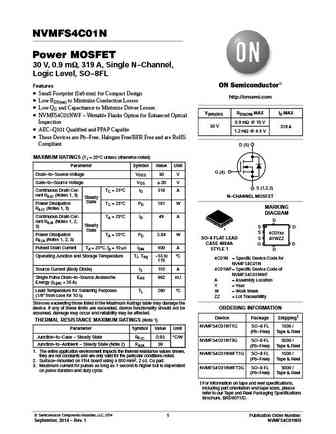
NVMFS4C01N Power MOSFET 30 V, 0.9 mW, 319 A, Single N-Channel, Logic Level, SO-8FL Features Small Footprint (5x6 mm) for Compact Design http //onsemi.com Low RDS(on) to Minimize Conduction Losses Low QG and Capacitance to Minimize Driver Losses V(BR)DSS RDS(ON) MAX ID MAX NVMFS4C01NWF - Wettable Flanks Option for Enhanced Optical 0.9 mW @ 10 V Inspection 30 V 319 A
nvmfs6h848nl.pdf
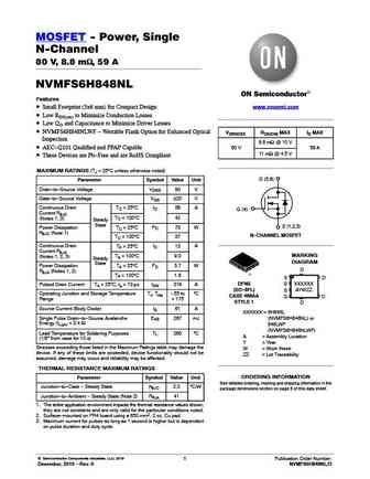
MOSFET - Power, Single N-Channel 80 V, 8.8 mW, 59 A NVMFS6H848NL Features www.onsemi.com Small Footprint (5x6 mm) for Compact Design Low RDS(on) to Minimize Conduction Losses Low QG and Capacitance to Minimize Driver Losses NVMFS6H848NLWF - Wettable Flank Option for Enhanced Optical V(BR)DSS RDS(ON) MAX ID MAX Inspection 8.8 mW @ 10 V AEC-Q101 Qualified and PPAP
nvmfs5c646nl.pdf
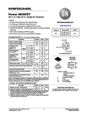
NVMFS5C646NL Power MOSFET 60 V, 4.7 mW, 93 A, Single N-Channel Features Small Footprint (5x6 mm) for Compact Design Low RDS(on) to Minimize Conduction Losses www.onsemi.com Low QG and Capacitance to Minimize Driver Losses NVMFS5C646NLWF - Wettable Flank Option for Enhanced Optical Inspection V(BR)DSS RDS(ON) MAX ID MAX AEC-Q101 Qualified and PPAP Capable 4.7 mW @
nvmfs5834nl.pdf
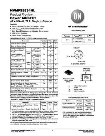
NVMFS5834NL Product Preview Power MOSFET 40 V, 9.3 mW, 76 A, Single N-Channel Features Small Footprint (5x6 mm) for Compact Design Low RDS(on) to Minimize Conduction Losses http //onsemi.com Low QG and Capacitance to Minimize Driver Losses AEC-Q101 Qualified These are Pb-Free Devices V(BR)DSS RDS(ON) MAX ID MAX MAXIMUM RATINGS (TJ = 25 C unless otherwise noted)
nvmfs4c310n.pdf
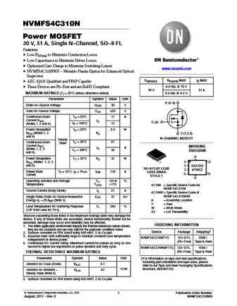
NVMFS4C310N Power MOSFET 30 V, 51 A, Single N-Channel, SO-8 FL Features Low RDS(on) to Minimize Conduction Losses Low Capacitance to Minimize Driver Losses Optimized Gate Charge to Minimize Switching Losses www.onsemi.com NVMFS4C310NWF - Wettable Flanks Option for Enhanced Optical Inspection V(BR)DSS RDS(ON) MAX ID MAX AEC-Q101 Qualified and PPAP Capable 6.0 mW @
nvmfs6h852nl.pdf

MOSFET - Power, Single N-Channel 80 V, 13.1 mW, 42 A NVMFS6H852NL Features Small Footprint (5x6 mm) for Compact Design www.onsemi.com Low RDS(on) to Minimize Conduction Losses Low QG and Capacitance to Minimize Driver Losses V(BR)DSS RDS(ON) MAX ID MAX NVMFS6H852NLWF - Wettable Flank Option for Enhanced Optical Inspection 13.1 mW @ 10 V 80 V 42 A AEC-Q101 Quali
nvmfs6h858n.pdf

MOSFET - Power, Single N-Channel 80 V, 20.7 mW, 32 A NVMFS6H858N Features www.onsemi.com Small Footprint (5x6 mm) for Compact Design Low RDS(on) to Minimize Conduction Losses Low QG and Capacitance to Minimize Driver Losses NVMFS6H858NWF - Wettable Flank Option for Enhanced Optical V(BR)DSS RDS(ON) MAX ID MAX Inspection 80 V 20.7 mW @ 10 V 32 A AEC-Q101 Qualifie
nvmfs5c450n.pdf
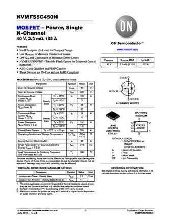
NVMFS5C450N MOSFET Power, Single N-Channel 40 V, 3.3 mW, 102 A Features www.onsemi.com Small Footprint (5x6 mm) for Compact Design Low RDS(on) to Minimize Conduction Losses Low QG and Capacitance to Minimize Driver Losses V(BR)DSS RDS(ON) MAX ID MAX NVMFS5C450NWF - Wettable Flank Option for Enhanced Optical 40 V 3.3 mW @ 10 V 102 A Inspection AEC-Q101 Qualif
nvmfs5113pl.pdf
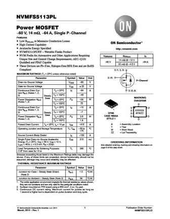
NVMFS5113PL Power MOSFET -60 V, 14 mW, -64 A, Single P-Channel Features Low RDS(on) to Minimize Conduction Losses High Current Capability Avalanche Energy Specified http //onsemi.com NVMFS5113PLWF - Wettable Flanks Product NVM Prefix for Automotive and Other Applications Requiring V(BR)DSS RDS(on) ID Unique Site and Control Change Requirements; AEC-Q101 14 mW @ -
nvmfs5826nl.pdf
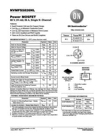
NVMFS5826NL Power MOSFET 60 V, 24 mW, 26 A, Single N-Channel Features Small Footprint (5x6 mm) for Compact Design Low RDS(on) to Minimize Conduction Losses http //onsemi.com Low QG and Capacitance to Minimize Driver Losses AEC-Q101 Qualified and PPAP Capable These are Pb-Free Devices and RoHS Compliant V(BR)DSS RDS(ON) MAX ID MAX 24 mW @ 10 V 60 V MAXIMUM RATINGS
ntmfs5844nlt1g nvmfs5844nl.pdf
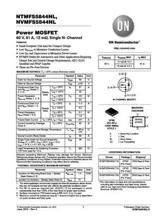
NTMFS5844NL, NVMFS5844NL Power MOSFET 60 V, 61 A, 12 mW, Single N-Channel Features Small Footprint (5x6 mm) for Compact Design http //onsemi.com Low RDS(on) to Minimize Conduction Losses Low QG and Capacitance to Minimize Driver Losses NVMFS Prefix for Automotive and Other Applications Requiring V(BR)DSS RDS(ON) MAX ID MAX Unique Site and Control Change Requirements;
nvmfs5c456n.pdf
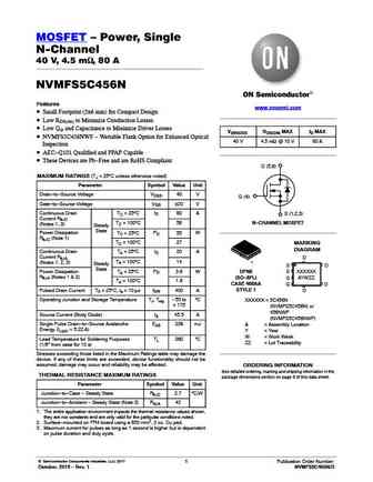
MOSFET Power, Single N-Channel 40 V, 4.5 mW, 80 A NVMFS5C456N Features www.onsemi.com Small Footprint (5x6 mm) for Compact Design Low RDS(on) to Minimize Conduction Losses Low QG and Capacitance to Minimize Driver Losses V(BR)DSS RDS(ON) MAX ID MAX NVMFS5C456NWF - Wettable Flank Option for Enhanced Optical 40 V 4.5 mW @ 10 V 80 A Inspection AEC-Q101 Qualifie
nvmfs024n06c.pdf
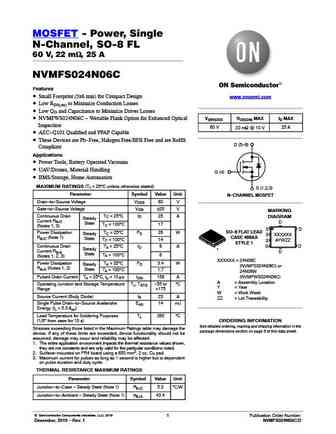
MOSFET - Power, Single N-Channel, SO-8 FL 60 V, 22 mW, 25 A NVMFS024N06C Features Small Footprint (5x6 mm) for Compact Design www.onsemi.com Low RDS(on) to Minimize Conduction Losses Low QG and Capacitance to Minimize Driver Losses NVMFWS024N06C - Wettable Flank Option for Enhanced Optical V(BR)DSS RDS(ON) MAX ID MAX Inspection 60 V 22 mW @ 10 V 25 A AEC-Q101 Qua
nvmfs5c410n.pdf

MOSFET - Power, Single N-Channel 40 V, 0.92 mW, 300 A NVMFS5C410N Features www.onsemi.com Small Footprint (5x6 mm) for Compact Design Low RDS(on) to Minimize Conduction Losses Low QG and Capacitance to Minimize Driver Losses NVMFS5C410NWF - Wettable Flank Option for Enhanced Optical V(BR)DSS RDS(ON) MAX ID MAX Inspection 40 V 0.92 mW @ 10 V 300 A AEC-Q101 Qualif
Другие IGBT... NVMFD5C680NL, NVMFD6H840NL, NVMFD6H846NL, NVMFD6H852NL, NVMFS015N10MCL, NVMFS016N06C, NVMFS020N06C, NVMFS024N06C, AON6414A, NVMFS4C302N, NVMFS4C310N, NVMFS5A140PLZ, NVMFS5A160PLZ, NVMFS5C406N, NVMFS5C406NL, NVMFS5C410N, NVMFS5C426N
History: PSMN012-80PS
🌐 : EN ES РУ

Список транзисторов
Обновления
MOSFET: FTF30P35D | FTF25N35DHVT | FTF15N35D | FTE15C35G | FTP02P15G | FTE02P15G | AKF30N5P0SX | AKF30N10S | AKF20P45D | CM4407 | CM3407 | CM3400 | SVF11N65F | SVF11N65T | FKBB3105 | EHBA036R1
Popular searches
2sc2580 | 2sc710 | 2sc968 | 2sd217 | bdw93c equivalent | cs7n60f | d613 transistor | fdmc8884 mosfet