SE100250GTS. Аналоги и основные параметры
Наименование производителя: SE100250GTS
Тип транзистора: MOSFET
Полярность: N
Предельные значения
Pd ⓘ - Максимальная рассеиваемая мощность: 400 W
|Vds|ⓘ - Максимально допустимое напряжение сток-исток: 100 V
|Vgs|ⓘ - Максимально допустимое напряжение затвор-исток: 20 V
|Id| ⓘ - Максимально допустимый постоянный ток стока: 250 A
Tj ⓘ - Максимальная температура канала: 175 °C
Электрические характеристики
tr ⓘ - Время нарастания: 85 ns
Cossⓘ - Выходная емкость: 1600 pf
RDSonⓘ - Сопротивление сток-исток открытого транзистора: 0.003 Ohm
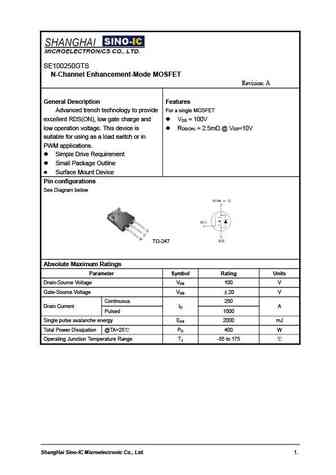
Тип корпуса: TO247
Аналог (замена) для SE100250GTS
- подборⓘ MOSFET транзистора по параметрам
SE100250GTS даташит
se100250gts.pdf
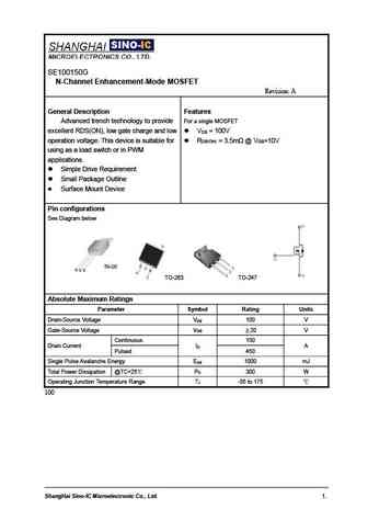
SE100250GTS N-Channel Enhancement-Mode MOSFET Revision A General Description Features For a single MOSFET Advanced trench technology to provide excellent RDS(ON), low gate charge and V = 100V DS low operation voltage. This device is R =2.5m @V =10V DS(ON) GS suitable for using as a load switch or in PWM applications. Simple Drive Requirement Small Package Outlin
se10080a.pdf
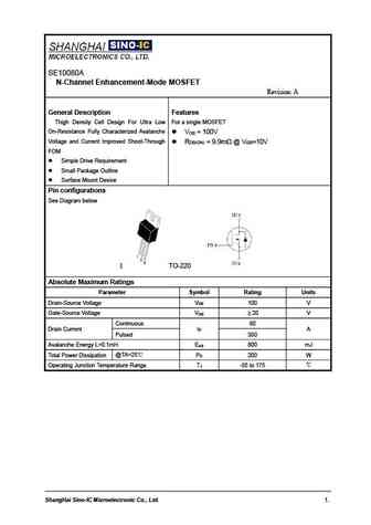
SE10080A N-Channel Enhancement-Mode MOSFET Revision A General Description Features Thigh Density Cell Design For Ultra Low For a single MOSFET On-Resistance Fully Characterized Avalanche V =100V DS Voltage and Current Improved Shoot-Through R =9.9m @V =10V DS(ON) GS FOM Simple Drive Requirement Small Package Outline Surface Mount Device Pin configurations
se100p60.pdf
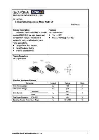
SE100P60 P-Channel Enhancement-Mode MOSFET Revision A General Description Features For a single MOSFET Advanced trench technology to provide excellent RDS(ON), low gate charge and V = -100V DS low operation voltage. This device is R =18m @V =-10V DS(ON) GS suitable for using as a load switch or in PWM applications. Simple Drive Requirement Small Package Outline
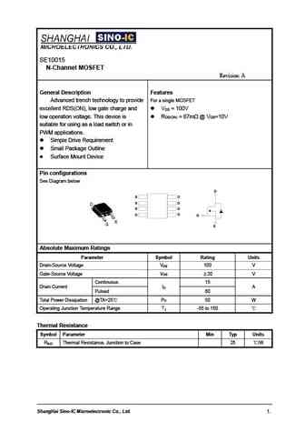
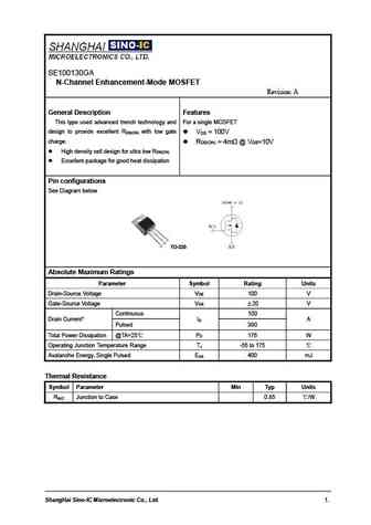
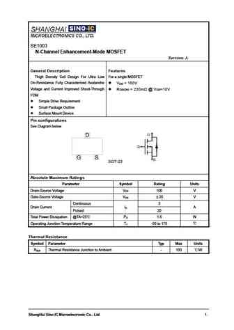
Другие MOSFET... MT7N65 , MT7N65-220F , SE01P13K , SE100130A , SE100130GA , SE10015 , SE100150G , SE100180GA , IRF1010E , SE1003 , SE10030A , SE10060A , SE10080A , SE100P60 , SE120120G , SE12060GA , SE1216 .
History: AP15N03GH
History: AP15N03GH
🌐 : EN ES РУ

Список транзисторов
Обновления
MOSFET: AUB034N10 | AUB033N08BG | AUB026N085 | AUA062N08BG | AUA060N08AG | AUA056N08BGL | AUA039N10 | ASW80R290E | ASW65R120EFD | ASW65R110E | ASW65R095EFD | ASW65R046EFD | ASW65R041EFDA | ASW65R041E | ASW60R150E | ASW60R090EFDA
Popular searches
2n3906 transistor equivalent | 2sc4883 | tip31a datasheet | d882 datasheet | tip29 transistor | s9014 transistor datasheet | 2sa1491 | 2sc1313 datasheet