SED3030M. Аналоги и основные параметры
Наименование производителя: SED3030M
Тип транзистора: MOSFET
Полярность: N
Предельные значения
Pd ⓘ - Максимальная рассеиваемая мощность: 40 W
|Vds|ⓘ - Максимально допустимое напряжение сток-исток: 30 V
|Vgs|ⓘ - Максимально допустимое напряжение затвор-исток: 20 V
|Id| ⓘ - Максимально допустимый постоянный ток стока: 30 A
Tj ⓘ - Максимальная температура канала: 175 °C
Электрические характеристики
tr ⓘ - Время нарастания: 12 ns
Cossⓘ - Выходная емкость: 102 pf
RDSonⓘ - Сопротивление сток-исток открытого транзистора: 0.0085 Ohm
Тип корпуса: DFN3X3EP
Аналог (замена) для SED3030M
- подборⓘ MOSFET транзистора по параметрам
SED3030M даташит
sed3030m.pdf
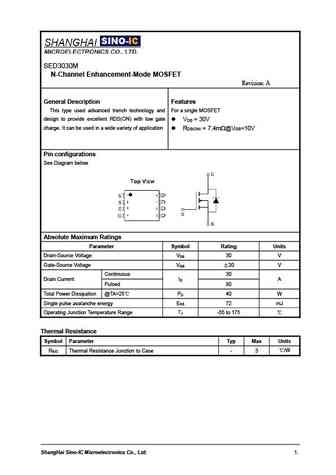
SED3030M N-Channel Enhancement-Mode MOSFET Revision A General Description Features This type used advanced trench technology and For a single MOSFET design to provide excellent RDS(ON) with low gate V =30V DS charge. It can be used in a wide variety of application R =7.4m @V =10V DS(ON) GS Pin configurations See Diagram below Absolute Maximum Ratings Parameter Symbol Ra
sed3032g.pdf
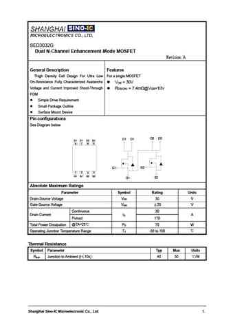
SED3032G Dual N-Channel Enhancement-Mode MOSFET Revision A General Description Features Thigh Density Cell Design For Ultra Low For a single MOSFET On-Resistance Fully Characterized Avalanche V =30V DS Voltage and Current Improved Shoot-Through R =7.4m @V =10V DS(ON) GS FOM Simple Drive Requirement Small Package Outline Surface Mount Device Pin configuratio
sed3022m.pdf
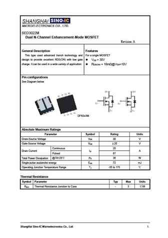
SED3022M Dual N-Channel Enhancement-Mode MOSFET Revision A General Description Features This type used advanced trench technology and For a single MOSFET design to provide excellent RDS(ON) with low gate V =30V DS charge. It can be used in a wide variety of application R =16m @V =10V DS(ON) GS Pin configurations See Diagram below DFN3x3M Absolute Maximum Ratings Parame
sed3080m.pdf
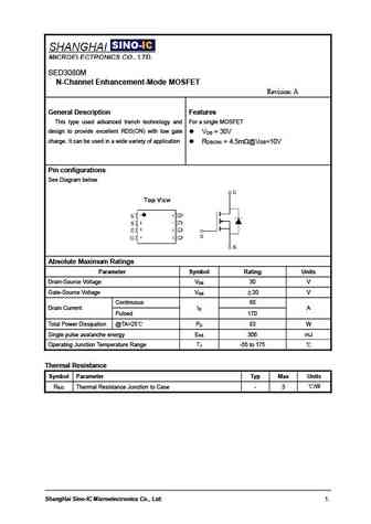
SED3080M N-Channel Enhancement-Mode MOSFET Revision A General Description Features This type used advanced trench technology and For a single MOSFET design to provide excellent RDS(ON) with low gate V =30V DS charge. It can be used in a wide variety of application R =4.5m @V =10V DS(ON) GS Pin configurations See Diagram below Absolute Maximum Ratings Parameter Symbol Ra

Другие MOSFET... SE8N65A , SE9435 , SE9926 , SED10070GG , SED10080GG , SED14N65G , SED2145 , SED3022M , IRFZ24N , SED3032G , SED3080M , SED3081M , SED30P30M , SED4060G , SED4060GM , SED5852 , SED8830A .
History: NTE4153NT1G | SI2325DS | NDT6N70 | IRF7700
History: NTE4153NT1G | SI2325DS | NDT6N70 | IRF7700
🌐 : EN ES РУ

Список транзисторов
Обновления
MOSFET: AUB034N10 | AUB033N08BG | AUB026N085 | AUA062N08BG | AUA060N08AG | AUA056N08BGL | AUA039N10 | ASW80R290E | ASW65R120EFD | ASW65R110E | ASW65R095EFD | ASW65R046EFD | ASW65R041EFDA | ASW65R041E | ASW60R150E | ASW60R090EFDA
Popular searches
2sb77 | ac128 transistor datasheet | c2878 transistor | 2sc732 | 2sc1451 replacement | 6426 mosfet | b1565 | nce82h140