80N10 datasheet, аналоги, основные параметры
Наименование производителя: 80N10 📄📄
Тип транзистора: MOSFET
Полярность: N
Предельные значения
Pd ⓘ - Максимальная рассеиваемая мощность: 250 W
|Vds|ⓘ - Максимально допустимое напряжение сток-исток: 100 V
|Vgs|ⓘ - Максимально допустимое напряжение затвор-исток: 20 V
|Id| ⓘ - Максимально допустимый постоянный ток стока: 100 A
Tj ⓘ - Максимальная температура канала: 175 °C
Электрические характеристики
tr ⓘ - Время нарастания: 90 ns
Cossⓘ - Выходная емкость: 665 pf
RDSonⓘ - Сопротивление сток-исток открытого транзистора: 0.0085 Ohm
Тип корпуса: TO220AB
📄📄 Копировать
Аналог (замена) для 80N10
- подборⓘ MOSFET транзистора по параметрам
80N10 даташит
80n10.pdf
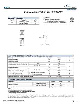
80N10 www.VBsemi.tw N-Channel 100-V (D-S) 175 C MOSFET FEATURES PRODUCT SUMMARY TrenchFET Power MOSFET VDS (V) RDS(on) ( )ID (A) 175 C Maximum Junction Temperature 0.0085 at VGS = 10 V 100 100 Compliant to RoHS Directive 2002/95/EC 0.010 at VGS = 6 V 85 TO-220AB D G S N-Channel MOSFET G D S ABSOLUTE MAXIMUM RATINGS TA = 25 C, unless otherwise noted Pa
gt080n10d5.pdf
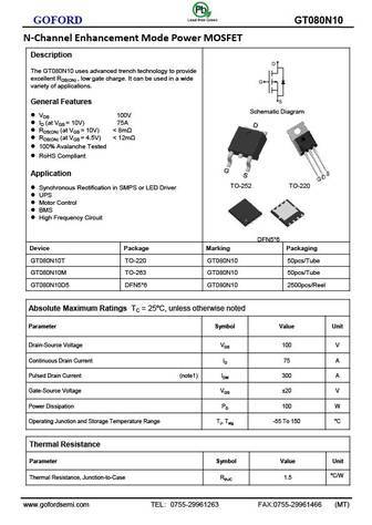
GOFORD GT080N10 N-Channel Enhancement Mode Power MOSFET Description The GT080N10 uses advanced trench technology to provide excellent RDS(ON) , low gate charge. It can be used in a wide variety of applications. General Features Schematic Diagram VDS 100V ID (at VGS = 10V) 75A RDS(ON) (at VGS = 10V)
s80n10r s80n10s.pdf
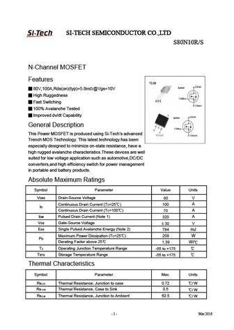
SI-TECH SEMICONDUCTOR CO.,LTD S80N10R/S N-Channel MOSFET Features 80V,100A,Rds(on)(typ)=5.8m @Vgs=10V High Ruggedness Fast Switching 100% Avalanche Tested Improved dv/dt Capability General Description This Power MOSFET is produced using Si-Tech s advanced Trench MOS Technology. This latest technology has been especially designed to minimize on-st
sth180n10f3-6.pdf
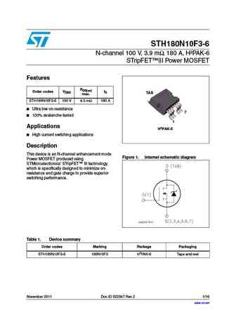
STH180N10F3-6 N-channel 100 V, 3.9 m , 180 A, H PAK-6 STripFET III Power MOSFET Features RDS(on) Order codes VDSS ID TAB max. STH180N10F3-6 100 V 4.5 m 180 A Ultra low on-resistance 7 100% avalanche tested 1 Applications H2PAK-6 High current switching applications Description This device is an N-channel enhancement mode Figure 1. Internal schematic diagra
sth80n10lf7-2ag.pdf
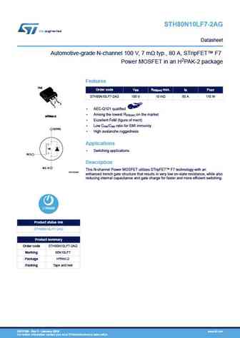
STH80N10LF7-2AG Datasheet Automotive-grade N-channel 100 V, 7 m typ., 80 A, STripFET F7 Power MOSFET in an H2PAK-2 package Features TAB VDS RDS(on) max. ID PTOT Order code STH80N10LF7-2AG 100 V 10 m 80 A 110 W 2 3 1 AEC-Q101 qualified Among the lowest RDS(on) on the market H2PAK-2 Excellent FoM (figure of merit) Low Crss/Ciss ratio for EMI immunity D(TA
ste180n10.pdf
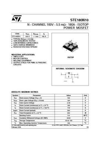
STE180N10 N - CHANNEL 100V - 5.5 m - 180A - ISOTOP POWER MOSFET TYPE VDSS RDS(on) ID STE180N10 100 V
sth180n10f3-2.pdf
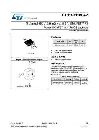
STH180N10F3-2 N-channel 100 V, 3.9 m typ.,180 A, STripFET F3 Power MOSFET in H PAK-2 package Datasheet - production data Features RDS(on) Order code VDS ID max. STH180N10F3-2 100 V 4.5 m 180 A Ultra low on-resistence 100% avalanche tested Applications Switching applications Figure 1 Internal schematic diagram Description This device is an N-cha
stp180n10f3.pdf
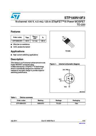
STP180N10F3 N-channel 100 V, 4.5 m , 120 A STripFET III Power MOSFET TO-220 Features RDS(on) TAB Order codes VDSS ID max. STP180N10F3 100 V 5.1 m 120 A Ultra low on-resistance 3 2 100% avalanche tested 1 TO-220 Applications High current switching applications Description This device is an N-channel enhancement mode Figure 1. Internal schematic diagram Po
std80n10f7 stf80n10f7 sth80n10f7-2 stp80n10f7.pdf
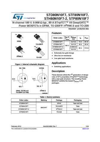
STD80N10F7, STF80N10F7, STH80N10F7-2, STP80N10F7 N-channel 100 V, 0.008 typ., 80 A STripFET VII DeepGATE Power MOSFETs in DPAK, TO-220FP, H2PAK-2 and TO-220 Datasheet - production data Features TAB VDS @ RDS(on) 3 Order codes ID PTOT TJmax max 1 DPAK 3 STD80N10F7 0.01 70 A 85 W 2 1 TO-220FP STF80N10F7 0.01 40 A 30 W 100 V TAB TAB STH80N10F7-2 0.0095 80 A
fdpf680n10t.pdf
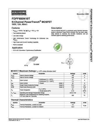
November 2008 FDPF680N10T N-Channel PowerTrench MOSFET 100V, 12A, 68m Features Description RDS(on) = 54m ( Typ.)@ VGS = 10V, ID = 6A This N-Channel MOSFET is produced using Fairchild Semicon- ductor s advanced PowerTrench process that has been espe- Fast Switching Speed cially tailored to minimize the on-state resistance and yet maintain superior switching performanc
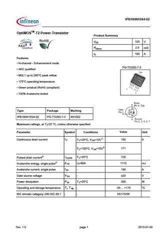
ipb180n10s4-03.pdf
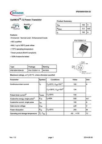
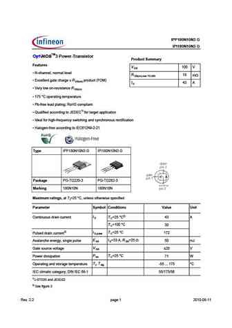
IPB180N10S4-03 OptiMOSTM-T2 Power-Transistor Product Summary VDS 100 V RDS(on) 3.3 mW ID 180 A Features N-channel - Normal Level - Enhancement mode PG-TO263-7-3 AEC qualified MSL1 up to 260 C peak reflow 175 C operating temperature Green product (RoHS compliant) 100% Avalanche tested Type Package Marking IPB180N10S4-03 PG-TO263-7-3 4N1003 Maximum ratin
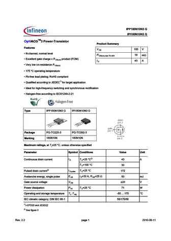
ipd180n10n3g.pdf
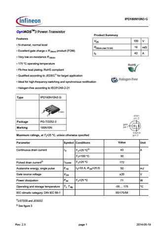
IPD180N10N3 G OptiMOSTM3 Power-Transistor Product Summary Features VDS 100 V N-channel, normal level RDS(on),max TO-263 18 mW Excellent gate charge x R product (FOM) DS(on) ID 43 A Very low on-resistance R DS(on) 175 C operating temperature Pb-free lead plating; RoHS compliant Qualified according to JEDEC1) for target application Ideal for hig
spb80n10lg.pdf
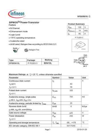
SPB80N10L SIPMOSTMPower-Transistor Product Summary Feature VDS S 2Hmfssjq R Jsmfshjrjsy rtij I Qtlnh Qj jq 627276 Marking Type Package XUG=5S 65Q Maximum Ratings1 fy Tj B 7 H1 zsqjxx tymjw nxj xujhnknji Parameter Symbol Value Unit
ipa180n10n3g.pdf
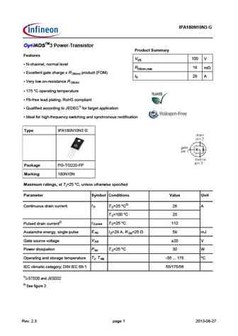
IPA180N10N3 G OptiMOSTM3 Power-Transistor Product Summary Features VDS 100 V N-channel, normal level RDS(on),max 18 mW Excellent gate charge x R product (FOM) DS(on) ID 28 A Very low on-resistance R DS(on) 175 C operating temperature Pb-free lead plating; RoHS compliant Qualified according to JEDEC1) for target application Ideal for high-freque
ipp180n10n3-g ipi180n10n3-g.pdf
IPP180N10N3 G IPI180N10N3 G OptiMOSTM3 Power-Transistor Product Summary Features V 100 V DS N-channel, normal level R 18 m DS(on),max TO-263 Excellent gate charge x R product (FOM) DS(on) I 43 A D Very low on-resistance R DS(on) 175 C operating temperature Pb-free lead plating; RoHS compliant Qualified according to JEDEC1) for target applicatio
ixfc80n10.pdf
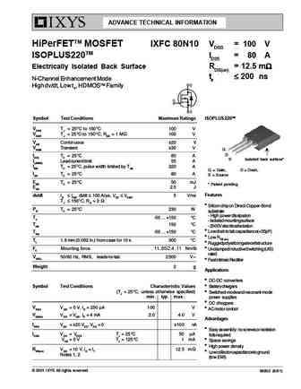
ADVANCE TECHNICAL INFORMATION HiPerFETTM MOSFET IXFC 80N10 VDSS = 100 V ISOPLUS220TM ID25 = 80 A Electrically Isolated Back Surface RDS(on) = 12.5 m trr 200 ns N-Channel Enhancement Mode High dv/dt, Low t , HDMOSTM Family rr Symbol Test Conditions Maximum Ratings ISOPLUS 220TM VDSS TJ = 25 C to 150 C 100 V VDGR TJ = 25 C to 150 C;
ixfd80n10.pdf
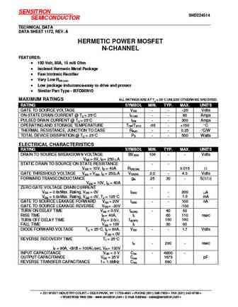
SENSITRON SHD224514 SEMICONDUCTOR TECHNICAL DATA DATA SHEET 1172, REV. A HERMETIC POWER MOSFET N-CHANNEL FEATURES 100 Volt, 80A, 15 mili Ohm Isolated Hermetic Metal Package Fast intrinsic Rectifier Very Low RDS (on) Low package inductance-easy to drive and protect Similar Part Type - IXFD80N10 MAXIMUM RATINGS ALL RATINGS ARE AT T = 25 C UNLESS OTHERWISE SPEC
ixfr180n10.pdf
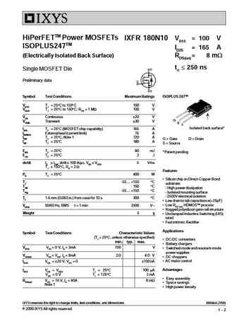
HiPerFETTM Power MOSFETs IXFR 180N10 VDSS = 100 V ISOPLUS247TM ID25 = 165 A (Electrically Isolated Back Surface) RDS(on)= 8 mW trr 250 ns Single MOSFET Die Preliminary data Symbol Test Conditions Maximum Ratings ISOPLUS 247TM VDSS TJ = 25 C to 150 C 100 V VDGR TJ = 25 C to 150 C; RGS = 1 MW 100 V VGS Continuous 20 V G VGSM Transient 30 V D Isolated back surface* ID25
ixth180n10t ixtq180n10t.pdf
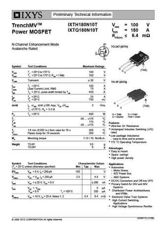
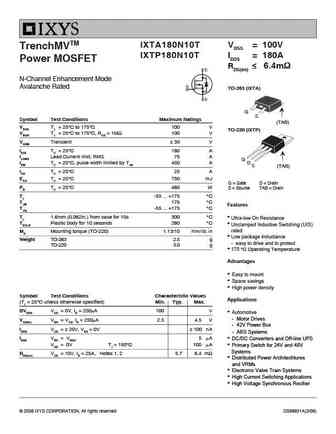
Preliminary Technical Information IXTH180N10T VDSS = 100 V TrenchMVTM IXTQ180N10T ID25 = 180 A Power MOSFET RDS(on) 6.4 m N-Channel Enhancement Mode TO-247 (IXTH) Avalanche Rated Symbol Test Conditions Maximum Ratings G (TAB) D VDSS TJ = 25 C to 175 C 100 V S VDGR TJ = 25 C to 175 C; RGS = 1 M 100 V VGSM Transient 30 V TO
ixtl2x180n10t.pdf
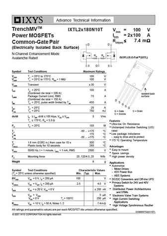
Advance Technical Information TrenchMVTM IXTL2x180N10T VDSS = 100 V ID25 = 2x100 A Power MOSFETs RDS(on) 7.4 m Common-Gate Pair DD (Electrically Isolated Back Surface) N-Channel Enhancement Mode RG RG ISOPLUS i5-PakTM (IXTL) Avalanche Rated S G S Symbol Test Conditions Maximum Ratings VDSS TJ = 25 C to 175 C 100 V VDGR TJ = 25 C to 175
ixfh80n10q ixft80n10q.pdf
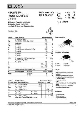
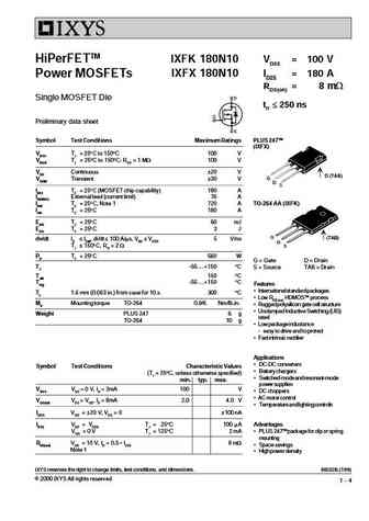
IXFH 80N10Q VDSS = 100 V HiPerFETTM IXFT 80N10Q ID25 = 80 A Power MOSFETs RDS(on) = 15 mW Q-Class trr 200ns N-Channel Enhancement Mode Avalanche Rated, High dV/dt Low Gate Charge and Capacitances Preliminary data TO-247 AD (IXFH) Symbol Test Conditions Maximum Ratings VDSS TJ = 25 C to 150 C 100 V VDGR TJ = 25 C to 150 C; RGS = 1 MW 100 V VGS Continuous 20 V VGSM Trans
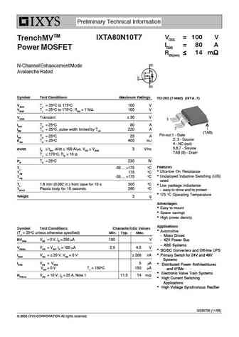
ixta80n10t ixtp80n10t.pdf
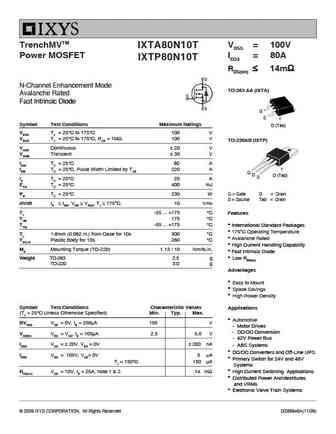
TrenchMVTM VDSS = 100V IXTA80N10T Power MOSFET ID25 = 80A IXTP80N10T RDS(on) 14m N-Channel Enhancement Mode TO-263 AA (IXTA) Avalanche Rated Fast Intrinsic Diode G S Symbol Test Conditions Maximum Ratings D (Tab) VDSS TJ = 25 C to 175 C 100 V VDGR TJ = 25 C to 175 C, RGS = 1M 100 V TO-220AB (IXTP) VGSS Continuous 20 V VGSM Transien
ixfa180n10t2 ixfp180n10t2.pdf
Preliminary Technical Information TrenchT2TM HiperFETTM VDSS = 100V IXFA180N10T2 Power MOSFET ID25 = 180A IXFP180N10T2 RDS(on) 6m N-Channel Enhancement Mode TO-263 AA (IXFA) Avalanche Rated Fast Intrinsic Rectifier G S D (Tab) Symbol Test Conditions Maximum Ratings VDSS TJ = 25 C to 175 C 100 V TO-220AB (IXFP) VDGR TJ = 25 C to 175 C, RG
ixfr80n10q.pdf
HiPerFETTM Power MOSFETs IXFR 80N10Q VDSS = 100 V ISOPLUS247TM, Q-Class ID25 = 76 A (Electrically Isolated Back Surface) RDS(on) = 15 mW N-Channel Enhancement Mode trr 200 ns Avalanche Rated Low Qg, High dv/dt Preliminary Data Sheet Symbol Test Conditions Maximum Ratings ISOPLUS 247TM E153432 VDSS TJ = 25 C to 150 C 100 V VDGR TJ = 25 C to 150 C; RGS = 1 MW 100 V VGS Cont
ixfn180n10.pdf
IXFN 180N10 VDSS = 100 V HiPerFETTM ID25 = 180 A Power MOSFET RDS(on) = 8 m Single MOSFET Die trr 250 ns Preliminary data sheet Symbol Test Conditions Maximum Ratings miniBLOC, SOT-227 B (IXFN) E153432 VDSS TJ = 25 C to 150 C 100 V S VDGR TJ = 25 C to 150 C, RGS = 1M 100 V G VGS Continuous 20 V VGSM Transient 30 V S ID
ixta180n10t7.pdf
PreliminaryTechnical Information VDSS = 100 V IXTA180N10T7 TrenchMVTM ID25 = 180 A Power MOSFET RDS(on) 6.4 m N-Channel Enhancement Mode Avalanche Rated Symbol Test Conditions Maximum Ratings TO-263 (7-lead) (IXTA..7) VDSS TJ = 25 C to 175 C 100 V VDGR TJ = 25 C to 175 C; RGS = 1 M 100 V VGSM Transient 30 V 1 ID25 TC = 25
ixta80n10t7.pdf
Preliminary Technical Information VDSS = 100 V IXTA80N10T7 TrenchMVTM ID25 = 80 A Power MOSFET RDS(on) 14 m N-Channel Enhancement Mode Avalanche Rated Symbol Test Conditions Maximum Ratings TO-263 (7-lead) (IXTA..7) VDSS TJ = 25 C to 175 C 100 V VDGR TJ = 25 C to 175 C; RGS = 1 M 100 V VGSM Transient 30 V 1 ID25 TC = 25 C80 A 7 I
ixta180n10t ixtp180n10t.pdf
IXTA180N10T VDSS = 100V TrenchMVTM IXTP180N10T ID25 = 180A Power MOSFET RDS(on) 6.4m N-Channel Enhancement Mode Avalanche Rated TO-263 (IXTA) G S Symbol Test Conditions Maximum Ratings (TAB) VDSS TJ = 25 C to 175 C 100 V TO-220 (IXTP) VDGR TJ = 25 C to 175 C, RGS = 1M 100 V VGSM Transient 30 V ID25 TC = 25 C 180 A ILRMS Lead Cur
ixfk180n10 ixfx180n10.pdf
HiPerFETTM IXFK 180N10 VDSS = 100 V IXFX 180N10 ID25 = 180 A Power MOSFETs RDS(on) = 8 mW Single MOSFET Die trr 250 ns Preliminary data sheet Symbol Test Conditions Maximum Ratings PLUS 247TM (IXFX) VDSS TJ = 25 C to 150 C 100 V VDGR TJ = 25 C to 150 C; RGS = 1 MW 100 V VGS Continuous 20 V D (TAB) G VGSM Transient 30 V D ID25 TC = 25 C (MOSFET chip capability) 180 A
ndpl180n10b ndpl180n10bg.pdf
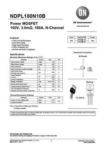
NDPL180N10B Power MOSFET www.onsemi.com 100V, 3.0m , 180A, N-Channel VDSS RDS(on) Max ID Max Features 3.0m @ 15V Ultra Low On-Resistance 100V 180A 3.5m @ 10V Low Gate Charge High Speed Switching 100% Avalanche Test Pb-Free and RoHS Compliance Electrical Connection Specifications N-Channel Absolute Maximum Ratings at Ta = 25 C Unit
ndba180n10b.pdf
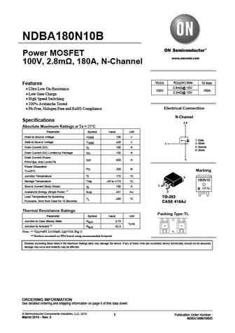
NDBA180N10B Power MOSFET www.onsemi.com 100V, 2.8m , 180A, N-Channel VDSS RDS(on) Max ID Max Features 2.8m @ 15V Ultra Low On-Resistance 100V 180A 3.3m @ 10V Low Gate Charge High Speed Switching 100% Avalanche Tested Electrical Connection Pb-Free, Halogen Free and RoHS Compliance N-Channel Specifications 2,4 Absolute Maximum Ratings at
fmb80n10t2 fmc80n10t2 fmi80n10t2.pdf
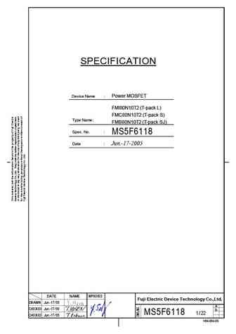
SPECIFICATION Device Name Power MOSFET FMI80N10T2 (T-pack L) FMC80N10T2 (T-pack S) Type Name FMB80N10T2 (T-pack SJ) Spec. No. MS5F6118 Date Jun.-17-2005 NAME DATE APPROVED Fuji Electric Device Technology Co.,Ltd. DRAWN Jun.-17-'05 a CHECKED Jun.-17-'05 b MS5F6118 1 / 22 CHECKED Jun.-17-'05 H04-004-05 This m aterial and the inform ation herein is the p roperty of Fuji E
jcs80n10i.pdf
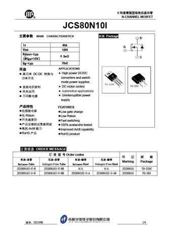
N N-CHANNEL MOSFET JCS80N10I MAIN CHARACTERISTICS Package ID 80A VDSS 100V Rdson-typ - 9.5m (@Vgs=10V Qg-typ 70nC APPLICATIONS High power DC/DC DC/DC converters and switch mode power supplies DC motor control Automotive ap
brcs080n10shzc.pdf
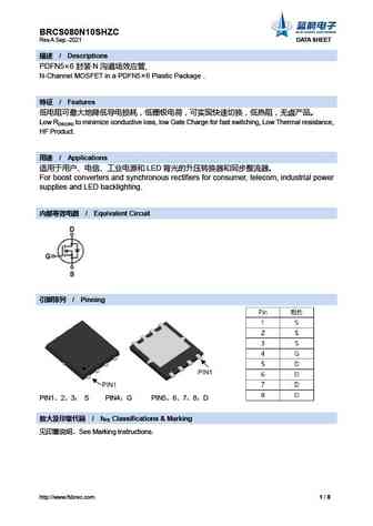
BRCS080N10SHZC Rev.A Sep.-2021 DATA SHEET / Descriptions PDFN5 6 N N-Channel MOSFET in a PDFN5 6 Plastic Package . / Features Low RDS(ON) to minimize conductive loss, low Gate Charge for fast switching, Low Thermal resistance
br80n10.pdf
BR80N10(BRCS80N10R) Rev.C Feb.-2015 DATA SHEET / Descriptions TO-220 N MOS N-CHANNEL MOSFET in a TO-220 Plastic Package. / Features , , Low gate charge, low crss, fast switching. / Applications DC/DC These devices are well suited for hig
brcs080n10shdp.pdf
BRCS080N10SHDP Rev.A Jul.-2022 DATA SHEET / Descriptions TO-252 N N-CHANNEL MOSFET in a TO-252 Plastic Package. / Features R C DS(on) rss Low RDS(on),low gate charge, low Crss, fast switching, HF Product. / Applications DC
brcs080n10shra.pdf
BRCS080N10SHRA Rev.B Sep.-2022 DATA SHEET / Descriptions TO-220 N N-CHANNEL MOSFET in a TO-220 Plastic Package. / Features , Ultra Low On-Resistance,fast switching. / Applications PFC . These de
brb80n10.pdf
BRB80N10(BRCS80N10B) Rev.C Feb.-2015 DATA SHEET / Descriptions TO-263 N MOS N-CHANNEL MOSFET in a TO-252 Plastic Package. / Features , , Low gate charge, low crss, fast switching. / Applications DC/DC These devices are well suited for hi
brcs080n10shbd.pdf
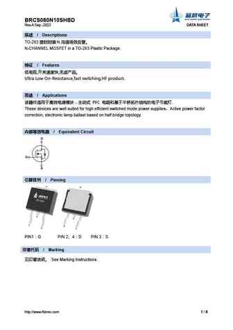
BRCS080N10SHBD Rev.A Sep.-2022 DATA SHEET / Descriptions TO-263 N N-CHANNEL MOSFET in a TO-263 Plastic Package. / Features , , Ultra Low On-Resistance,fast switching,HF product. / Applications PFC
ftk80n10p.pdf
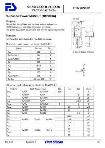
SEMICONDUCTOR FTK80N10P TECHNICAL DATA N-Channel Power MOSFET (100V/80A) Purpose Suited for low voltage applications such as automotive, DC/DC Converters, and high efficiency switching for power management in portable and battery operated products Feature Low RDS(on),low gate charge,low Crss,fast switching. Absolute maximum ratings(Ta=25 ) Symbol Rating Unit 1.Gate 2.Drain
dhs180n10l dhs180n10lf dhs180n10li dhs180n10le dhs180n10lb dhs180n10ld.pdf
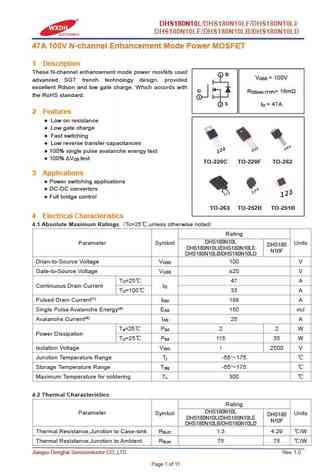
DHS180N10L/DHS180N10LF/DHS180N10LI/ DHS180N10LE/DHS180N10LB/DHS180N10LD 47A 100V N-channel Enhancement Mode Power MOSFET 1 Description These N-channel enhancement mode power mosfets used 2 D V = 100V DSS advanced SGT trench technology design, provided excellent Rdson and low gate charge. Which accords with G R = 18m DS(on) (TYP) the RoHS standard. 1 3 S I = 47A D 2 Features
dhs180n10ld.pdf
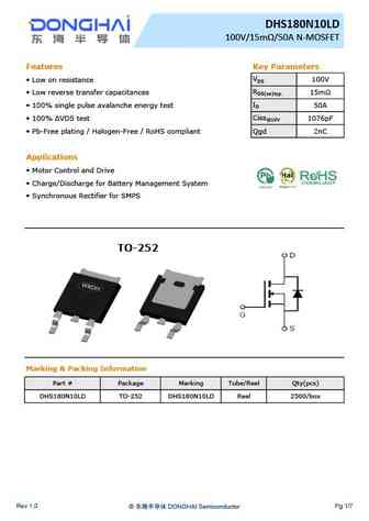
DHS180N10LD 100V/15m /50A N-MOSFET Features Key Parameters VDS Low on resistance 100V RDS(on)typ. Low reverse transfer capacitances 15m ID 100% single pulse avalanche energy test 50A Ciss@10V 100% VDS test 1076pF Pb-Free plating / Halogen-Free / RoHS compliant Qgd 2nC Applications Motor Control and Drive Charge/Discharge for Battery Management Sy
hyg080n10ls1d.pdf
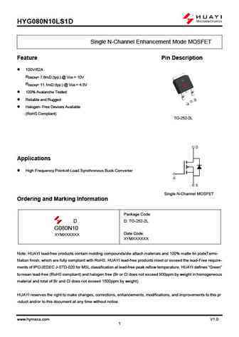
HYG080N10LS1D Single N-Channel Enhancement Mode MOSFET Feature Pin Description 100V/62A RDS(ON)= 7.6m (typ.) @ VGS = 10V RDS(ON)= 11.1m (typ.) @ VGS = 4.5V 100% Avalanche Tested Reliable and Rugged Halogen- Free Devices Available (RoHS Compliant) TO-252-2L Applications High Frequency Point-of-Load Synchronous Buck Converter Single N-Channel MOSF
ncep080n10f.pdf
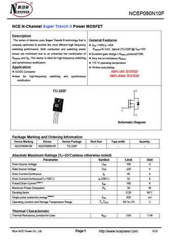
NCEP080N10F NCE N-Channel Super Trench II Power MOSFET Description The series of devices uses Super Trench II technology that is General Features uniquely optimized to provide the most efficient high frequency VDS =100V,ID =45A switching performance. Both conduction and switching power RDS(ON)=8.1m , typical (TO-220F)@ VGS=10V losses are minimized due to an extremely low
ncep080n10.pdf

NCEP080N10 NCE N-Channel Super Trench II Power MOSFET Description The series of devices uses Super Trench II technology that is General Features uniquely optimized to provide the most efficient high frequency VDS =100V,ID =75A switching performance. Both conduction and switching power RDS(ON)=7.4m , typical (TO-220)@ VGS=10V losses are minimized due to an extremely low co
ncep080n10a.pdf
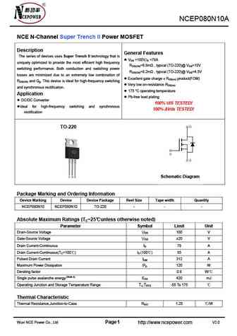
NCEP080N10A NCE N-Channel Super Trench II Power MOSFET Description General Features The series of devices uses Super Trench II technology that is VDS =100V,ID =78A uniquely optimized to provide the most efficient high frequency RDS(ON)=6.8m , typical (TO-220)@ VGS=10V switching performance. Both conduction and switching power RDS(ON)=8.2m , typical (TO-220)@ VGS=4.5V
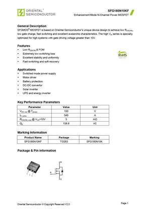

hrp180n10k.pdf
December 2014 BVDSS = 100 V RDS(on) typ =15 m HRP180N10K ID = 65 A 100V N-Channel Trench MOSFET TO-220 FEATURES Originative New Design Superior Avalanche Rugged Technology 1 2 3 Excellent Switching Characteristics 1.Gate 2. Drain 3. Source Unrivalled Gate Charge 85 nC (Typ.) Extended Safe Operating Area Lower RDS(ON) 15 m (Typ.)
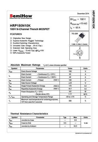
hrs180n10k.pdf
Oct 2016 BVDSS = 100 V RDS(on) typ = 15 HRS180N10K ID = 65 A 100V N-Channel Trench MOSFET TO-220F FEATURES Originative New Design Superior Avalanche Rugged Technology 1 2 3 Excellent Switching Characteristics 1.Gate 2. Drain 3. Source Unrivalled Gate Charge 85 nC (Typ.) Extended Safe Operating Area Lower RDS(ON) 15 (Typ.) @VGS=10V 100% Avalanche Tested
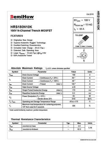
hrlo180n10k.pdf
Jan 2016 HRLO180N10K 100V N-Channel Trench MOSFET Features Key Parameters Parameter Value Unit High Dense Cell Design BVDSS 100 V Reliable and Rugged ID 9.3 A Advanced Trench Process Technology RDS(on), typ @10V 16 RDS(on), typ @4.5V 17 Application Package & Internal Circuit Power Management in Inverter System SOP-8 Synchronous Rectification Absolute Maximum Ratings
hrd180n10k hru180n10k.pdf
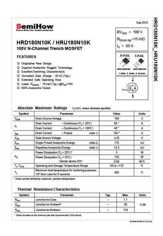
Sep 2015 BVDSS = 100 V RDS(on) typ =15 HRD180N10K / HRU180N10K ID = 65 A 100V N-Channel Trench MOSFET D-PAK I-PAK FEATURES 2 1 Originative New Design 1 3 2 3 Superior Avalanche Rugged Technology HRD180N10K HRU180N10K Excellent Switching Characteristics 1.Gate 2. Drain 3. Source Unrivalled Gate Charge 85 nC (Typ.) Extended Safe Operating Area Lower RDS(ON)
hrlf180n10k.pdf
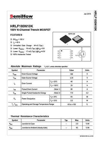
Jan 2016 HRLF180N10K 100V N-Channel Trench MOSFET 8DFN 5x6 FEATURES BVDSS = 100 V ID = 40 A 1 Unrivalled Gate Charge 94 nC (Typ.) Lower RDS(ON) 16 (Typ.) @VGS=10V Lower RDS(ON) 17 (Typ.) @VGS=4.5V 100% Avalanche Tested Absolute Maximum Ratings TJ=25 unless otherwise specified Symbol Parameter Value Units VDSS Drain-Source Voltage 100 V VGS Gate-Source Voltage
sl80n10.pdf
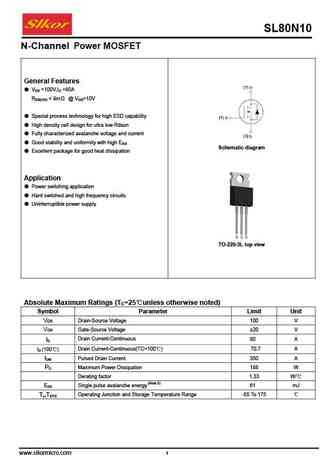
SL80N10 N-Channel Power MOSFET General Features VDS =100V,ID =80A RDS(ON)
wmu080n10hg2.pdf
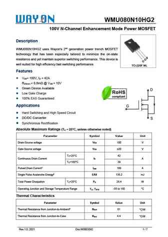
WMU080N10HG2 100V N-Channel Enhancement Mode Power MOSFET Description WMU080N10HG2 uses Wayon's 2nd generation power trench MOSFET technology that has been especially tailored to minimize the on-state S resistance and yet maintain superior switching performance. This device is GD well suited for high efficiency fast switching performance. TO-220F NL Features V = 100V, I =
wml080n10hg2.pdf
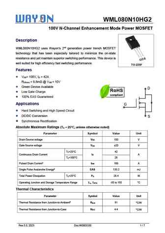
WML080N10HG2 100V N-Channel Enhancement Mode Power MOSFET Description WML080N10HG2 uses Wayon's 2nd generation power trench MOSFET technology that has been especially tailored to minimize the on-state resistance and yet maintain superior switching performance. This device is GDS well suited for high efficiency fast switching performance. TO-220F Features V = 100V, I = 42A
wmb080n10lg2.pdf
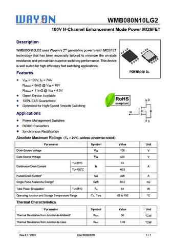
WMB080N10LG2 100V N-Channel Enhancement Mode Power MOSFET Description D D D D WMB080N10LG2 uses Wayon's 2nd generation power trench MOSFET D D D D technology that has been especially tailored to minimize the on-state G ss resistance and yet maintain superior switching performance. This device s ss G s is well suited for high efficiency fast switching applications. PDFN
wmo080n10hg2.pdf
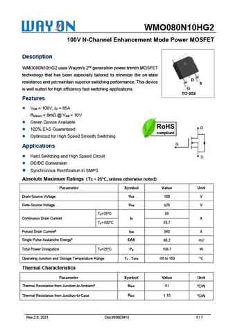
WMO080N10HG2 100V N-Channel Enhancement Mode Power MOSFET Description WMO080N10HG2 uses Wayon's 2nd generation power trench MOSFET technology that has been especially tailored to minimize the on-state D resistance and yet maintain superior switching performance. This device S G is well suited for high efficiency fast switching applications. TO-252 Features V = 100V, I =
fir80n10lg.pdf
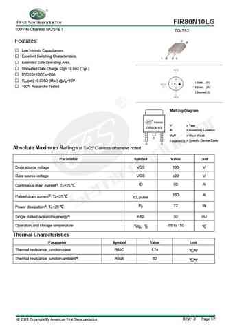
FIR80N10LG 100V N-Channel MOSFET TO-252 Features Low Intrinsic Capacitances. Excellent Switching Characteristics. Extended Safe Operating Area. Unrivalled Gate Charge Qg= 19.8nC (Typ.). BVDSS=100V,ID=80A RDS(on) 0.035 (Max) @VG=10V 1.Gate (G) 100% Avalanche Tested 2.Drain (D) 3.Sourse (S) Marking Diagram YAWW Y = Year FIR80N10L A = Assembly
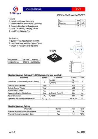
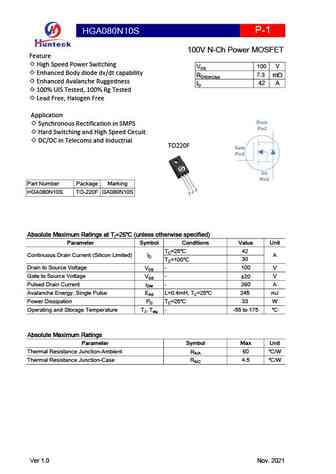
hga080n10a.pdf
P-1 HGA080N10A 100V N-Ch Power MOSFET Feature 100 V VDS High Speed Power Switching 7.6 RDS(on),typ VGS=10V mW Enhanced Body diode dv/dt capability 43.5 A ID (Sillicon Limited) Enhanced Avalanche Ruggedness 100% UIS Tested, 100% Rg Tested Lead Free, Halogen Free Application Synchronous Rectification in SMPS Drain Hard Switching and High Speed Circuit
hgd080n10a hgi080n10a.pdf
, P-1 HGD080N10A HGI080N10A 100V N-Ch Power MOSFET Feature 100 V VDS High Speed Power Switching 6.7 RDS(on),typ mW Enhanced Body diode dv/dt capability 88 A ID Enhanced Avalanche Ruggedness 100% UIS Tested, 100% Rg Tested Lead Free, Halogen Free Application Synchronous Rectification in SMPS Drain Hard Switching and High Speed Circuit DC/DC in
hga080n10al.pdf
HGA080N10AL P-1 100V N-Ch Power MOSFET Feature 100 V VDS High Speed Power Switching, Logic Level 7.1 RDS(on),typ VGS=10V mW Enhanced Body diode dv/dt capability 9.3 RDS(on),typ VGS=4.5V mW Enhanced Avalanche Ruggedness 45 A ID (Sillicon Limited) 100% UIS Tested, 100% Rg Tested Lead Free, Halogen Free Application Synchronous Rectification in SMPS Drain
hgs080n10sl.pdf
HGS080N10SL P-1 100V N-Ch Power MOSFET Feature 100 V VDS High Speed Power Switching,Logic level 7 RDS(on),typ VGS=10V mW Enhanced Body diode dv/dt capability 8.5 RDS(on),typ VGS=4.5V mW Enhanced Avalanche Ruggedness 14 A ID 100% UIS Tested, 100% Rg Tested Lead Free, Halogen Free Drain Application Synchronous Rectification in SMPS Hard Switching an
hgs080n10al.pdf

HGS080N10AL P-1 100V N-Ch Power MOSFET Feature 100 V VDS High Speed Power Switching,Logic level 7 RDS(on),typ VGS=10V mW Enhanced Body diode dv/dt capability 9.0 RDS(on),typ VGS=4.5V mW Enhanced Avalanche Ruggedness 14.4 A ID 100% UIS Tested, 100% Rg Tested Lead Free, Halogen Free Drain Application Synchronous Rectification in SMPS Hard Switching
hgd080n10al hgi080n10al.pdf
HGD080N10AL , P-1 HGI080N10AL 100V N-Ch Power MOSFET Feature 100 V VDS High Speed Power Switching, Logic Level 7.0 RDS(on),typ VGS=10V mW Enhanced Body diode dv/dt capability 9.1 RDS(on),typ VGS=4.5V mW Enhanced Avalanche Ruggedness 83 A ID (Sillicon Limited) 100% UIS Tested, 100% Rg Tested 70 A ID (Package Limited) Lead Free, Halogen Free Application
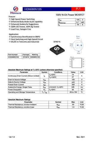
hgn080n10sl.pdf
HGN080N10SL P-1 100V N-Ch Power MOSFET Feature 100 V VDS High Speed Power Switching, Logic Level 6.1 RDS(on),typ VGS=10V mW Enhanced Body diode dv/dt capability 7.6 RDS(on),typ VGS=4.5V mW Enhanced Avalanche Ruggedness 74 A ID (Sillicon Limited) 100% UIS Tested, 100% Rg Tested 60 A ID (Package Limited) Lead Free, Halogen Free Application Synchronous Re
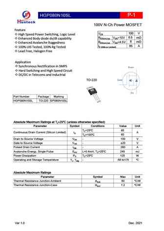
hgp080n10s.pdf
HGP080N10S P-1 100V N-Ch Power MOSFET Feature High Speed Power Switching 100 V VDS Enhanced Body diode dv/dt capability 7.1 RDS(on),typ mW Enhanced Avalanche Ruggedness 82 A ID 100% UIS Tested, 100% Rg Tested Lead Free, Halogen Free Application Drain Synchronous Rectification in SMPS Pin2 Hard Switching and High Speed Circuit DC/DC in Telecoms
hgn080n10al.pdf

HGN080N10AL P-1 100V N-Ch Power MOSFET Feature 100 V VDS High Speed Power Switching, Logic Level 6.5 RDS(on),typ VGS=10V mW Enhanced Body diode dv/dt capability 8.8 RDS(on),typ VGS=4.5V mW Enhanced Avalanche Ruggedness 74.4 A ID (Sillicon Limited) 100% UIS Tested, 100% Rg Tested 60 A ID (Package Limited) Lead Free, Halogen Free Application Synchronous
hgb080n10al hgp080n10al.pdf
HGB080N10AL , HGP080N10AL P-1 100V N-Ch Power MOSFET Feature 100 V VDS High Speed Power Switching, Logic Level 6.9 RDS(on),typ VGS=10V mW Enhanced Body diode dv/dt capability 9 RDS(on),typ VGS=4.5V mW Enhanced Avalanche Ruggedness 7.1 RDS(on),typ VGS=10V mW 100% UIS Tested, 100% Rg Tested 9.3 RDS(on),typ VGS=4.5V mW Lead Free, Halogen Free 85 A ID (Sillico
hgn080n10a.pdf
P-1 HGN080N10A 100V N-Ch Power MOSFET Feature 100 V VDS High Speed Power Switching 6.8 RDS(on),typ mW Enhanced Body diode dv/dt capability 76 A ID Enhanced Avalanche Ruggedness 100% UIS Tested, 100% Rg Tested Lead Free, Halogen Free Application Synchronous Rectification in SMPS Drain Hard Switching and High Speed Circuit DC/DC in Telecoms and I
hgb080n10a hgp080n10a.pdf
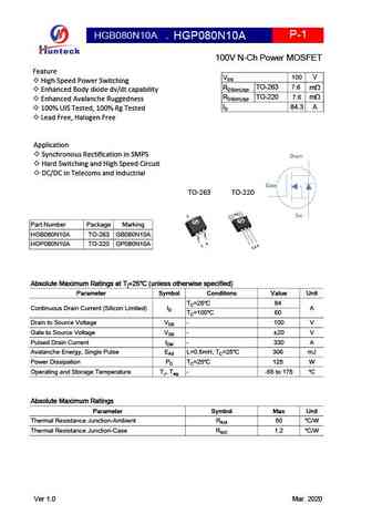
, P-1 HGB080N10A HGP080N10A 100V N-Ch Power MOSFET Feature 100 V VDS High Speed Power Switching TO-263 7.6 RDS(on),typ mW Enhanced Body diode dv/dt capability TO-220 7.6 RDS(on),typ mW Enhanced Avalanche Ruggedness 84.3 A ID 100% UIS Tested, 100% Rg Tested Lead Free, Halogen Free Application Synchronous Rectification in SMPS Drain Hard Switching
hgn080n10s.pdf
HGN080N10S P-1 100V N-Ch Power MOSFET Feature High Speed Power Switching 100 V VDS Enhanced Body diode dv/dt capability 6.7 RDS(on),typ mW Enhanced Avalanche Ruggedness 74 A ID 100% UIS Tested, 100% Rg Tested Lead Free, Halogen Free Application Drain Synchronous Rectification in SMPS Pin2 Hard Switching and High Speed Circuit DC/DC in Telecoms
hga080n10s.pdf
HGA080N10S P-1 100V N-Ch Power MOSFET Feature High Speed Power Switching 100 V VDS Enhanced Body diode dv/dt capability 7.3 RDS(on),typ mW Enhanced Avalanche Ruggedness 42 A ID 100% UIS Tested, 100% Rg Tested Lead Free, Halogen Free Application Drain Synchronous Rectification in SMPS Pin2 Hard Switching and High Speed Circuit DC/DC in Telecoms
wsr80n10.pdf
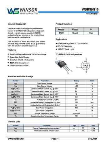
WSR80N10 N-Ch MOSFET General Description Product Summery The WSR80N10 is the highest performance ID BVDSS RDSON trench N-Ch MOSFET with extreme high cell density , which provide excellent RDSON 100V 10m 85A and gate charge for most of the synchronous buck converter applications . Applications The WSR80N10 meet the RoHS and Green Power Management in TV Converter. Pr
vbze80n10.pdf
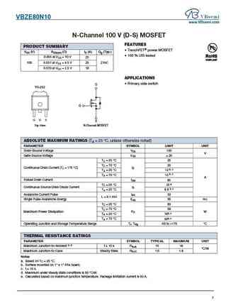
VBZE80N10 www.VBsemi.com N-Channel 100 V (D-S) MOSFET FEATURES PRODUCT SUMMARY TrenchFET power MOSFET VDS (V) RDS(on) ( )ID (A) Qg (Typ.) 100 % UIS tested 0.055 at VGS = 10 V 25 0.057 at VGS = 4.5 V 100 25 21nC 0.070 at VGS = 2.5 V 18 APPLICATIONS Primary side switch D TO-252 G G D S S N-Channel MOSFET Top View ABSOLUTE MAXIMUM RATINGS (TA = 25 C, unl
vbzm80n10.pdf
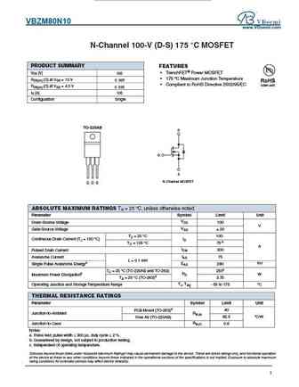
VBZM80N10 www.VBsemi.com N-Channel 100-V (D-S) 175 C MOSFET PRODUCT SUMMARY FEATURES VDS (V) TrenchFET Power MOSFET 100 175 C Maximum Junction Temperature RDS(on) ( ) at VGS = 10 V 0.009 Compliant to RoHS Directive 2002/95/EC RDS(on) ( ) at VGS = 4.5 V 0.020 ID (A) 100 Configuration Single TO-220AB D G S N-Channel MOSFET G D S ABSOLUTE MAXIMUM RATIN
utt80n10.pdf
UTT80N10 www.VBsemi.tw N-Channel 100-V (D-S) 175 C MOSFET FEATURES PRODUCT SUMMARY TrenchFET Power MOSFET VDS (V) RDS(on) ( )ID (A) 175 C Maximum Junction Temperature 0.0085 at VGS = 10 V 100 100 Compliant to RoHS Directive 2002/95/EC 0.010 at VGS = 6 V 85 TO-220AB D G S N-Channel MOSFET G D S ABSOLUTE MAXIMUM RATINGS TA = 25 C, unless otherwise not
s80n10r s80n10s s80n10rn s80n10rp.pdf
S80N10R/S/RN/RP SI-TECH SEMICONDUCTOR CO.,LTD N-Channel Power MOSFET Features Applications VDS=80V,ID=100A DC Motor Control Rds(on)(typ)=6.3m @Vgs=10V DC-DC Converters 100% Avalanche Tested BMS 100% Rg Tested SMPS Lead-Free (RoHS Compliant) Automotive Environment Internal Circuit and Pin Description D D G G G G G D D D
hms80n10ka.pdf
HMS80N10KA N-Channel Super Trench Power MOSFET Description The HMS80N10AL uses Super Trench technology that is uniquely optimized to provide the most efficient high frequency switching performance. Both conduction and switching power losses are minimized due to an extremely low combination of RDS(ON) and Qg. This device is ideal for high-frequency switching and synchronous rectif
hms80n10.pdf
HMS80N10 N-Channel Super Trench Power MOSFET Description The HMS80N10 uses Super Trench technology that is uniquely optimized to provide the most efficient high frequency switching performance. Both conduction and switching power losses are minimized due to an extremely low combination of RDS(ON) and Qg. This device is ideal for high-frequency switching and synchronous rectificat
hms80n10al.pdf
HMS80N10AL N-Channel Super Trench Power MOSFET Description The uses Super Trench technology that is uniquely optimized to provide the most efficient high frequency switching performance. Both conduction and switching power losses are minimized due to an extremely low combination of RDS(ON) and Qg. This device is ideal for high-frequency switching and synchronous rectif
hms80n10d.pdf
HMS80N10D N-Channel Super Trench Power MOSFET Description The HMS80N10D uses Super Trench technology that is uniquely optimized to provide the most efficient high frequency switching performance. Both conduction and switching power losses are minimized due to an extremely low combination of RDS(ON) and Qg. This device is ideal for high-frequency switching and synchronous rectific
sfp080n100ac2 sfb077n100ac2.pdf
SFP080N100AC2,SFB077N100AC2 N-MOSFET 100V, 6.5m , 110A Features Product Summary Low On-Resistance VDS 100V Fast Switching RDS(on) typ. 6.5m 100% Avalanche Tested Repetitive Avalanche Allowed up to Tjmax ID 110A Lead-Free, RoHS Compliant 100% DVDS Tested Applications Power management for inverter systems 100% Avalanche Tested Synchronous rectification SFP08
mpg180n10p mpg180n10s.pdf
100V N-Channel Power MOSFET DESCRIPTION The MPG180N10P uses advanced trench technology to provide excellent R , low gate charge. It can be used in DS(ON) a wide variety of applications. KEY CHARACTERISTICS V = 100V,I = 180A R
ipi180n10n3.pdf
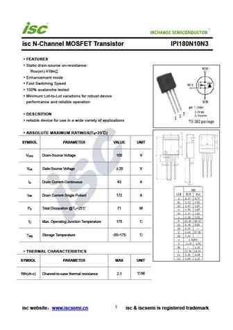
INCHANGE Semiconductor isc N-Channel MOSFET Transistor IPI180N10N3 FEATURES Static drain-source on-resistance RDS(on) 18m Enhancement mode Fast Switching Speed 100% avalanche tested Minimum Lot-to-Lot variations for robust device performance and reliable operation DESCRITION reliable device for use in a wide variety of applications ABSOLUTE MAXIMUM RATINGS(T
ipd180n10n3.pdf
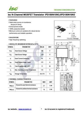
isc N-Channel MOSFET Transistor IPD180N10N3,IIPD180N10N3 FEATURES Static drain-source on-resistance RDS(on) 18m Enhancement mode 100% avalanche tested Minimum Lot-to-Lot variations for robust device performance and reliable operation DESCRITION High frequency switching ABSOLUTE MAXIMUM RATINGS(T =25 ) a SYMBOL PARAMETER VALUE UNIT V Drain-Source Voltage 100
sth80n10lf7.pdf
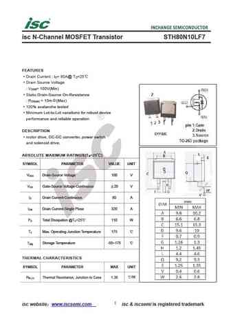
isc N-Channel MOSFET Transistor STH80N10LF7 FEATURES Drain Current I = 80A@ T =25 D C Drain Source Voltage V = 100V(Min) DSS Static Drain-Source On-Resistance R = 10m (Max) DS(on) 100% avalanche tested Minimum Lot-to-Lot variations for robust device performance and reliable operation DESCRIPTION motor drive, DC-DC converter, power switch and solenoid drive.
ixtp80n10t.pdf
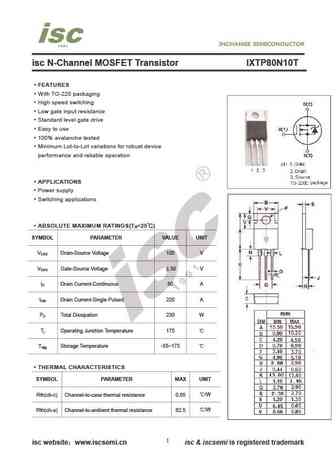
isc N-Channel MOSFET Transistor IXTP80N10T FEATURES With TO-220 packaging High speed switching Low gate input resistance Standard level gate drive Easy to use 100% avalanche tested Minimum Lot-to-Lot variations for robust device performance and reliable operation APPLICATIONS Power supply Switching applications ABSOLUTE MAXIMUM RATINGS(T =25 ) a SYMBOL P
ixfa180n10t2.pdf
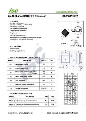
INCHANGE Semiconductor isc N-Channel MOSFET Transistor IXFA180N10T2 FEATURES With TO-263( D2PAK ) packaging High speed switching Low gate input resistance Standard level gate drive Easy to use 100% avalanche tested Minimum Lot-to-Lot variations for robust device performance and reliable operation APPLICATIONS Power supply Switching applications ABSOLUTE MAX
ipp180n10n3.pdf
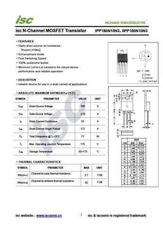
INCHANGE Semiconductor isc N-Channel MOSFET Transistor IPP180N10N3 IIPP180N10N3 FEATURES Static drain-source on-resistance RDS(on) 18m Enhancement mode Fast Switching Speed 100% avalanche tested Minimum Lot-to-Lot variations for robust device performance and reliable operation DESCRITION reliable device for use in a wide variety of applications ABSOLUTE
ipa180n10n3.pdf
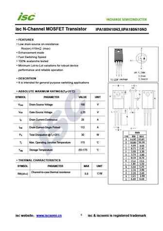
isc N-Channel MOSFET Transistor IPA180N10N3,IIPA180N10N3 FEATURES Low drain-source on-resistance RDS(on) 18m (max) Enhancement mode Fast Switching Speed 100% avalanche tested Minimum Lot-to-Lot variations for robust device performance and reliable operation DESCRITION It is intended for general purpose switching applications ABSOLUTE MAXIMUM RATINGS(T =25 )
fdpf680n10t.pdf
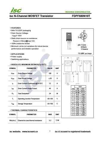
isc N-Channel MOSFET Transistor FDPF680N10T FEATURES With TO-220F packaging Drain Source Voltage- V 100V DSS Static drain-source on-resistance RDS(on) 68m @V =10V GS 100% avalanche tested Minimum Lot-to-Lot variations for robust device performance and reliable operation APPLICATIONS Power supply Switching applications ABSOLUTE MAXIMUM RATINGS(T =2
stp80n10f7.pdf
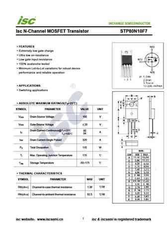
INCHANGE Semiconductor Isc N-Channel MOSFET Transistor STP80N10F7 FEATURES Extremely low gate charge Ultra low on-resistance Low gate input resistance 100% avalanche tested Minimum Lot-to-Lot variations for robust device performance and reliable operation APPLICATIONS Switching applications ABSOLUTE MAXIMUM RATINGS(T =25 ) a SYMBOL PARAMETER VALUE UNIT V Drain-
ap280n10mp.pdf
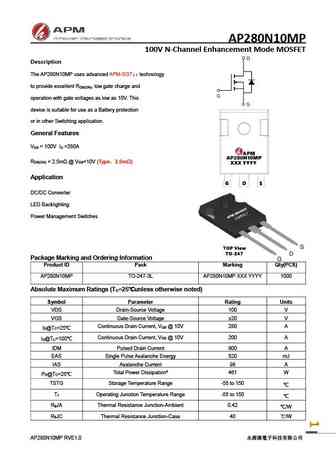
AP280N10MP 100V N-Channel Enhancement Mode MOSFET Description The AP280N10MP uses advanced APM-SGT technology to provide excellent R , low gate charge and DS(ON) operation with gate voltages as low as 10V. This device is suitable for use as a Battery protection or in other Switching application. General Features V = 100V I =280A DS D R
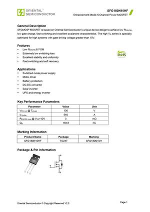
apg80n10nf.pdf
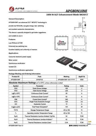
APG80N10NF 100V N-SGT Enhancement Mode MOSFET General Description APG80N10NF use advanced SGT MOSFET technology to provide low RDS(ON), low gate charge, fast switching and excellent avalanche characteristics. This device is specially designed to get better ruggedness and suitable to use in Features Low RDS(on) & FOM Extremely low switching loss Excellent stability and uni
apg80n10p apg80n10t.pdf
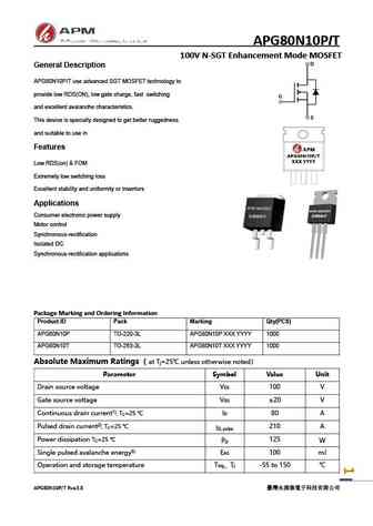
APG80N10PIT 100V N-SGT Enhancement Mode MOSFET General Description APG80N10P/T use advanced SGT MOSFET technology to provide low RDS(ON), low gate charge, fast switching and excellent avalanche characteristics. This device is specially designed to get better ruggedness and suitable to use in Features Low RDS(on) & FOM Extremely low switching loss Excellent stability and u
ap180n10mp.pdf
AP180N10MP 100V N-Channel Enhancement Mode MOSFET Description The AP180N10MP uses advanced APM-SGT technology to provide excellent R , low gate charge and DS(ON) operation with gate voltages as low as 10V. This device is suitable for use as a Battery protection or in other Switching application. General Features V = 100V I =180A DS D R
ap80n10p ap80n10t.pdf
AP80N10PIT 100V N-Channel Enhancement Mode MOSFET Description The AP80N10P/T uses advanced APM-SGT technology to provide excellent R , low gate charge and DS(ON) operation with gate voltages as low as 10V. This device is suitable for use as a Battery protection or in other Switching application. General Features V = 100V I =80A DS D R
Другие IGBT... 2SK1623, 2SK2158-T1B, 30N06L, 30N06-TO220, 30N06-TO252, 30N20, 30P06, 70N06L-TQ2, CS150N03A8, AF2301PWL, AF4502CSLA, AFN3404S23RG, AFN4172WSS8, AFP2307AS23, AM20P06-135, AM2319P-T1, AM2336N-T1
Параметры MOSFET. Взаимосвязь и компромиссы
History: IPU105N03LG | 3SK63 | JMSL1006PGS | JMSL1008AE | DG2N60-220F | NP55N04SUG | DH025N03I
🌐 : EN ES РУ

Список транзисторов
Обновления
MOSFET: CS95118 | CS85105A | CS75N45 | CS72N12 | CS55N50 | CS48N75A | CS40N27 | MSQ60P04D | MSQ40P07D | MSQ30P40D | MSQ30P15 | MSQ30P07D | MSQ100N03D | MSHM60P14 | MSHM40N085 | MSHM30N46
Popular searches
c5149 datasheet | m1830m mosfet | pkch2bb mosfet | 2024ont | 2n1306 transistor | 2sa750 datasheet | 2sa940 transistor datasheet | 2sb549