NCEP065N85. Аналоги и основные параметры
Наименование производителя: NCEP065N85
Тип транзистора: MOSFET
Полярность: N
Предельные значения
Pd ⓘ - Максимальная рассеиваемая мощность: 120 W
|Vds|ⓘ - Максимально допустимое напряжение сток-исток: 85 V
|Vgs|ⓘ - Максимально допустимое напряжение затвор-исток: 20 V
|Id| ⓘ - Максимально допустимый постоянный ток стока: 90 A
Tj ⓘ - Максимальная температура канала: 175 °C
Электрические характеристики
tr ⓘ - Время нарастания: 11 ns
Cossⓘ - Выходная емкость: 483 pf
RDSonⓘ - Сопротивление сток-исток открытого транзистора: 0.0065 Ohm
Тип корпуса: TO220
Аналог (замена) для NCEP065N85
- подборⓘ MOSFET транзистора по параметрам
NCEP065N85 даташит
ncep065n85 ncep065n85d.pdf

NCEP065N85,NCEP065N85D NCE N-Channel Super Trench II Power MOSFET Description The series of devices uses Super Trench II technology that is General Features uniquely optimized to provide the most efficient high frequency VDS =85V,ID =90A switching performance. Both conduction and switching power RDS(ON)=5.9m , typical (TO-220)@ VGS=10V losses are minimized due to an extre
ncep065n85.pdf
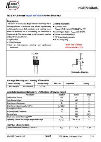
NCEP065N85 NCE N-Channel Super Trench II Power MOSFET Description The series of devices uses Super Trench II technology that is General Features uniquely optimized to provide the most efficient high frequency VDS =85V,ID =90A switching performance. Both conduction and switching power RDS(ON)=5.7m , typical (TO-220)@ VGS=10V losses are minimized due to an extremely low com
ncep065n85d.pdf
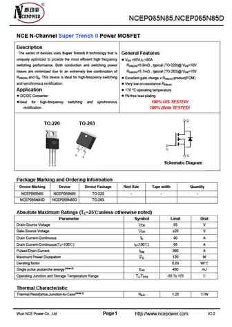
NCEP065N85,NCEP065N85D NCE N-Channel Super Trench II Power MOSFET Description The series of devices uses Super Trench II technology that is General Features uniquely optimized to provide the most efficient high frequency VDS =85V,ID =90A switching performance. Both conduction and switching power RDS(ON)=5.9m , typical (TO-220)@ VGS=10V losses are minimized due to an extre
ncep065n12agu.pdf
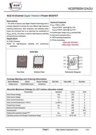
NCEP065N12AGU NCE N-Channel Super Trench II Power MOSFET Description General Features The series of devices uses Super Trench II technology that is V =120V,I =100A DS D uniquely optimized to provide the most efficient high frequency R =5.6m , typical @ V =10V DS(ON) GS switching performance. Both conduction and switching power R =6.9m , typical @ V =4.5V DS(ON) GS losses ar
Другие MOSFET... NCEP045N10 , NCEP045N10D , NCEP050N85 , NCEP050N85D , NCEP055N85 , NCEP055N85D , NCEP058N85 , NCEP058N85D , 5N65 , NCEP068N10AG , NCEP068N10AK , NCEP068N10G , NCEP072N10 , NCEP12T12 , NCEP12T12D , NCEP1520 , NCEP1545G .
🌐 : EN ES РУ

Список транзисторов
Обновления
MOSFET: AUB062N08BG | AUB060N08AG | AUB056N10 | AUB056N08BGL | AUB050N085 | AUB050N055 | AUB045N12 | AUB045N10BT | AUB039N10 | AUB034N10 | AUB033N08BG | AUB026N085 | AUA062N08BG | AUA060N08AG | AUA056N08BGL | AUA039N10
Popular searches
irfp460 характеристики | k2837 datasheet | k389 transistor | mje15032g equivalent | nsd134 | 60r190p datasheet | cs30n20 datasheet | go42n10