FDD86102LZ datasheet, аналоги, основные параметры
Наименование производителя: FDD86102LZ 📄📄
Тип транзистора: MOSFET
Полярность: N
Предельные значения
Pd ⓘ - Максимальная рассеиваемая мощность: 54 W
|Vds|ⓘ - Максимально допустимое напряжение сток-исток: 100 V
|Vgs|ⓘ - Максимально допустимое напряжение затвор-исток: 20 V
|Id| ⓘ - Максимально допустимый постоянный ток стока: 42 A
Tj ⓘ - Максимальная температура канала: 150 °C
Электрические характеристики
RDSonⓘ - Сопротивление сток-исток открытого транзистора: 0.0225 Ohm
📄📄 Копировать
Аналог (замена) для FDD86102LZ
- подборⓘ MOSFET транзистора по параметрам
FDD86102LZ даташит
fdd86102lz.pdf
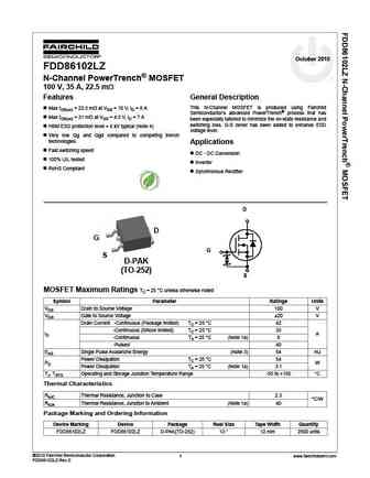
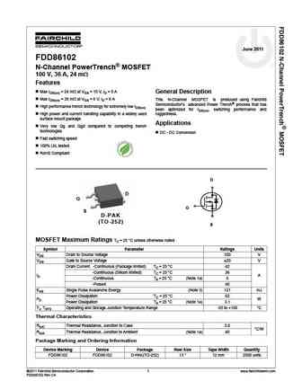
October 2010 FDD86102LZ N-Channel PowerTrench MOSFET 100 V, 35 A, 22.5 m Features General Description This N-Channel MOSFET is produced using Fairchild Max rDS(on) = 22.5 m at VGS = 10 V, ID = 8 A Semiconductor s advanced PowerTrench process that has Max rDS(on) = 31 m at VGS = 4.5 V, ID = 7 A been especially tailored to minimize the on-state resistance and switching
fdd86102lz.pdf

Is Now Part of To learn more about ON Semiconductor, please visit our website at www.onsemi.com Please note As part of the Fairchild Semiconductor integration, some of the Fairchild orderable part numbers will need to change in order to meet ON Semiconductor s system requirements. Since the ON Semiconductor product management systems do not have the ability to manage part nomenclatur
fdd86102lz.pdf
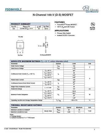
FDD86102LZ www.VBsemi.tw N-Channel 100-V (D-S) MOSFET FEATURES PRODUCT SUMMARY TrenchFET Power MOSFET VDS (V) RDS(on) ( ) ID (A)a Qg (Typ.) 100 % Rg and UIS Tested 0.0185 at VGS = 10 V 100 60 38 nC APPLICATIONS Primary Side Switch Isolated DC/DC Converter TO-252 D G S G D S Top View N-Channel MOSFET ABSOLUTE MAXIMUM RATINGS (TA = 25 C, unless
fdd86102lz.pdf
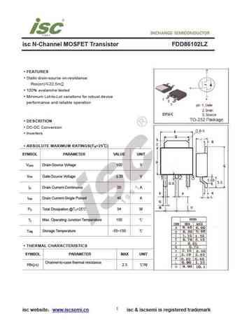
isc N-Channel MOSFET Transistor FDD86102LZ FEATURES Static drain-source on-resistance RDS(on) 22.5m 100% avalanche tested Minimum Lot-to-Lot variations for robust device performance and reliable operation DESCRITION DC-DC Conversion Inverters ABSOLUTE MAXIMUM RATINGS(T =25 ) a SYMBOL PARAMETER VALUE UNIT V Drain-Source Voltage 100 V DSS V Gate-Source Volta


Другие IGBT... FDD8447LF085, FDD8451, FDD8453LZ, FDD8453LZF085, FDD850N10L, STT02N07, FDD86102, STT01N20, IRLB4132, STT01L10, FDD86250, FDD86326, FDD8647L, FDD8770, FDD8778, FDD8780, FDD8782
Параметры MOSFET. Взаимосвязь и компромиссы
🌐 : EN ES РУ

Список транзисторов
Обновления
MOSFET: CS95118 | CS85105A | CS75N45 | CS72N12 | CS55N50 | CS48N75A | CS40N27 | MSQ60P04D | MSQ40P07D | MSQ30P40D | MSQ30P15 | MSQ30P07D | MSQ100N03D | MSHM60P14 | MSHM40N085 | MSHM30N46
Popular searches
2n3905 | mj15023 | tip36c transistor | 2sc3320 | 2sc2078 | ac127 transistor | a42 transistor | bc547c