FDS9945. Аналоги и основные параметры
Наименование производителя: FDS9945
Тип транзистора: MOSFET
Полярность: N
Предельные значения
Pd ⓘ
- Максимальная рассеиваемая мощность: 2 W
|Vds|ⓘ - Максимально допустимое напряжение сток-исток: 60 V
|Vgs|ⓘ - Максимально допустимое напряжение затвор-исток: 20 V
|Id| ⓘ - Максимально допустимый постоянный ток стока: 3.5 A
Tj ⓘ - Максимальная температура канала: 175 °C
Электрические характеристики
tr ⓘ -
Время нарастания: 4.3 ns
Cossⓘ - Выходная емкость: 48 pf
RDSonⓘ - Сопротивление сток-исток открытого транзистора: 0.1 Ohm
Тип корпуса: SO-8
Аналог (замена) для FDS9945
- подборⓘ MOSFET транзистора по параметрам
FDS9945 даташит
..1. Size:73K fairchild semi
fds9945.pdf 
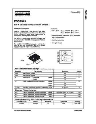
February 2001 FDS9945 60V N-Channel PowerTrench MOSFET General Description Features 3.5 A, 60 V. R = 0.100 @ V = 10 V DS(ON) GS These N Channel Logic Level MOSFET have been R = 0.200 @ V = 4.5V DS(ON) GS designed specifically to improve the overall efficiency of DC/DC converters using either synchronous or Optimized for use in switching DC/DC converters co
..2. Size:169K onsemi
fds9945.pdf 
Is Now Part of To learn more about ON Semiconductor, please visit our website at www.onsemi.com ON Semiconductor and the ON Semiconductor logo are trademarks of Semiconductor Components Industries, LLC dba ON Semiconductor or its subsidiaries in the United States and/or other countries. ON Semiconductor owns the rights to a number of patents, trademarks, copyrights, trade secrets, and oth
0.1. Size:913K cn vbsemi
fds9945-nl.pdf 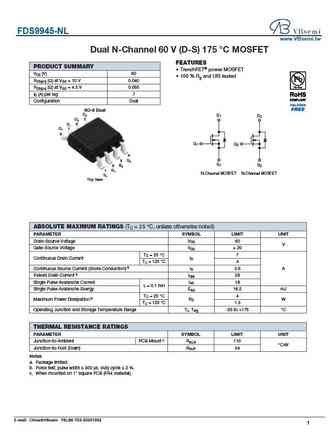
FDS9945-NL www.VBsemi.tw Dual N-Channel 60 V (D-S) 175 C MOSFET FEATURES PRODUCT SUMMARY TrenchFET power MOSFET VDS (V) 60 100 % Rg and UIS tested RDS(on) ( ) at VGS = 10 V 0.040 RDS(on) ( ) at VGS = 4.5 V 0.055 ID (A) per leg 7 Configuration Dual SO-8 Dual D2 D1 D2 D2 5 D1 6 D1 7 8 G1 G2 4 G2 3 3 S1 S2 S2 S2 2 2 G G1 1 1 N-Channel MOSFET N-Chann
9.1. Size:162K fairchild semi
fds9934c.pdf 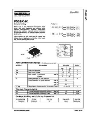
March 2006 FDS9934C Complementary Features These dual N- and P-Channel enhancement mode Q1 6.5 A, 20 V. RDS(ON) = 30 m @ VGS = 4.5 V power field effect transistors are produced using RDS(ON) = 43 m @ VGS = 2.5 V. Fairchild Semiconductor s advanced PowerTrench process that has been especially tailored to minimize on-state ressitance and yet maintain superior switching perf
9.2. Size:339K fairchild semi
fds9958.pdf 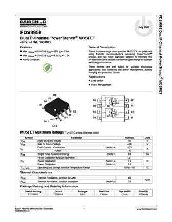
July 2007 FDS9958 tm Dual P-Channel PowerTrench MOSFET -60V, -2.9A, 105m Features General Description Max rDS(on) =105m at VGS = -10V, ID = -2.9A These P-channel logic level specified MOSFETs are produced using Fairchild Semiconductor s advanced PowerTrench Max rDS(on) =135m at VGS = -4.5V, ID = -2.5A process that has been especially tailored to minimize the RoHS
9.3. Size:116K fairchild semi
fds9926a.pdf 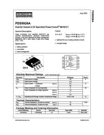
July 2003 FDS9926A Dual N-Channel 2.5V Specified PowerTrench MOSFET Features General Description These N-Channel 2.5V specified MOSFETs use 6.5 A, 20 V. RDS(ON) = 30 m @ VGS = 4.5 V Fairchild Semiconductor s advanced PowerTrench RDS(ON) = 43 m @ VGS = 2.5 V. process. It has been optimized for power management applications with a wide range of gate drive voltage Optimized
9.4. Size:292K fairchild semi
fds9933bz.pdf 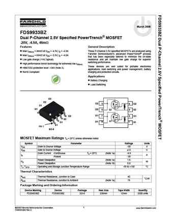
March 2008 FDS9933BZ tm Dual P-Channel 2.5V Specified PowerTrench MOSFET -20V, -4.9A, 46m Features General Description Max rDS(on) = 46m at VGS = -4.5V, ID = -4.9A These P-Channel 2.5V specified MOSFETs are produced using Fairchild Semiconductor s advanced PowerTrench process Max rDS(on) = 69m at VGS = -2.5V, ID = -4.0A that has been especially tailored to minimize
9.5. Size:367K fairchild semi
fds9933.pdf 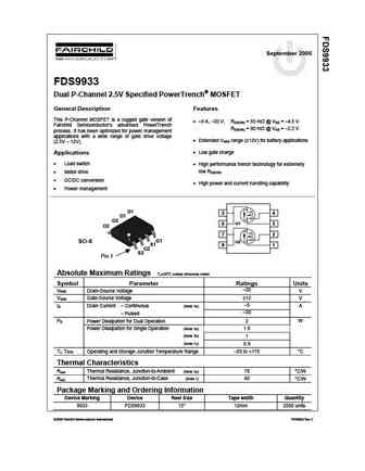
September 2006 FDS9933 Dual P-Channel 2.5V Specified PowerTrench MOSFET General Description Features This P-Channel MOSFET is a rugged gate version of 5 A, 20 V, RDS(ON) = 55 m @ VGS = 4.5 V Fairchild Semiconductor s advanced PowerTrench RDS(ON) = 90 m @ VGS = 2.5 V process. It has been optimized for power management applications with a wide range of ga
9.6. Size:63K fairchild semi
fds9933a.pdf 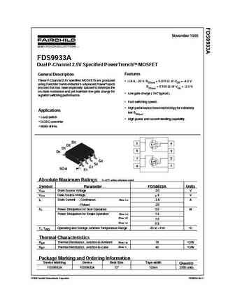
November 1998 FDS9933A Dual P-Channel 2.5V Specified PowerTrench MOSFET Features General Description These P-Channel 2.5V specified MOSFETs are produced -3.8 A, -20 V. RDS(on) = 0.075 @ VGS = -4.5 V using Fairchild Semiconductor's advanced PowerTrench RDS(on) = 0.105 @ VGS = -2.5 V. process that has been especially tailored to minimize the on-state resistance and yet ma
9.7. Size:549K fairchild semi
fds9958 f085.pdf 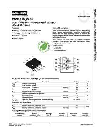
November 2008 FDS9958_F085 Dual P-Channel PowerTrench MOSFET -60V, -2.9A, 105m Features General Description Max rDS(on) =105m at VGS = -10V, ID = -2.9A These P-channel logic level specified MOSFETs are produced using Fairchild Semiconductor s advanced PowerTrench Max rDS(on) =135m at VGS = -4.5V, ID = -2.5A process that has been especially tailored to minimize the o
9.8. Size:73K fairchild semi
fds9953a.pdf 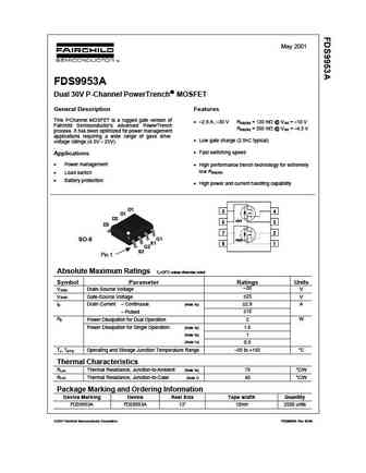
May 2001 FDS9953A Dual 30V P-Channel PowerTrench MOSFET General Description Features This P MOSFET is a rugged gate version of -Channel 2.9 A, 30 V R = 130 m @ V = 10 V DS(ON) GS Fairchild Semiconductor s advanced PowerTrench R = 200 m @ V = 4.5 V DS(ON) GS process. It has been optimized for power management applications requiring a wide range of g
9.9. Size:272K onsemi
fds9934c.pdf 
Is Now Part of To learn more about ON Semiconductor, please visit our website at www.onsemi.com Please note As part of the Fairchild Semiconductor integration, some of the Fairchild orderable part numbers will need to change in order to meet ON Semiconductor s system requirements. Since the ON Semiconductor product management systems do not have the ability to manage part nomenclatur
9.10. Size:334K onsemi
fds9958.pdf 
Is Now Part of To learn more about ON Semiconductor, please visit our website at www.onsemi.com Please note As part of the Fairchild Semiconductor integration, some of the Fairchild orderable part numbers will need to change in order to meet ON Semiconductor s system requirements. Since the ON Semiconductor product management systems do not have the ability to manage part nomenclatur
9.11. Size:854K cn vbsemi
fds9926a.pdf 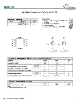
FDS9926A www.VBsemi.tw Dual N-Channel 20-V (D-S) MOSFET FEATURES PRODUCT SUMMARY Halogen-free According to IEC 61249-2-21 VDS (V) RDS(on) ( )ID (A) Definition 0.025 at VGS = 4.5 V 7.1 TrenchFET Power MOSFET 20 0.035 at VGS = 2.5 V 6.0 100 % Rg Tested Compliant to RoHS Directive 2002/95/EC SO-8 D1 D2 S1 1 D1 8 G1 2 D1 7 S2 3 D2 6 G1 G2 G2 4 D2
9.12. Size:1522K cn vbsemi
fds9933a.pdf 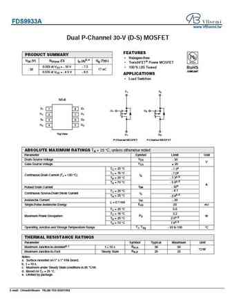
FDS9933A www.VBsemi.tw Dual P-Channel 30-V (D-S) MOSFET FEATURES PRODUCT SUMMARY Halogen-free VDS (V) RDS(on) ( ) ID (A)d, e Qg (Typ.) TrenchFET Power MOSFET 0.029 at VGS = - 10 V - 7.3 100 % UIS Tested RoHS - 30 17 nC COMPLIANT 0.039 at VGS = - 4.5 V - 6.3 APPLICATIONS Load Switches S1 S2 SO-8 S1 1 D1 8 G1 G2 G1 2 D1 7 S2 3 D2 6 G2 4 D2 5 Top Vie
Другие MOSFET... SDU06N60
, FDS9400A
, FDS9431A
, FDS9431AF085
, FDS9926A
, FDS9933BZ
, FDS9934C
, SDU05N04
, IRFZ44N
, FDS9953A
, FDS9958
, FDS9958F085
, FDSS2407
, FDT3612
, SDU04N65
, FDT3N40
, SDU04N60
.
