NCEP031N85M datasheet, аналоги, основные параметры
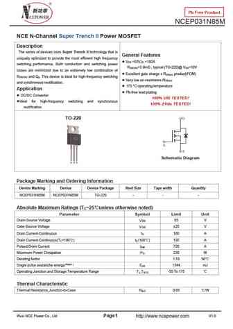
Наименование производителя: NCEP031N85M
Тип транзистора: MOSFET
Полярность: N
Предельные значения
Pd ⓘ
- Максимальная рассеиваемая мощность: 230 W
|Vds|ⓘ - Максимально допустимое напряжение сток-исток: 85 V
|Vgs|ⓘ - Максимально допустимое напряжение затвор-исток: 20 V
|Id| ⓘ - Максимально допустимый постоянный ток стока: 180 A
Tj ⓘ - Максимальная температура канала: 175 °C
Электрические характеристики
tr ⓘ -
Время нарастания: 15 ns
Cossⓘ - Выходная емкость: 1350 pf
RDSonⓘ - Сопротивление сток-исток открытого транзистора: 0.0031 Ohm
Тип корпуса: TO-220
Аналог (замена) для NCEP031N85M
- подборⓘ MOSFET транзистора по параметрам
NCEP031N85M даташит
..1. Size:997K ncepower
ncep031n85m.pdf 

Pb Free Product NCEP031N85M NCE N-Channel Super Trench II Power MOSFET Description The series of devices uses Super Trench II technology that is General Features uniquely optimized to provide the most efficient high frequency V =85V,I =180A DS D switching performance. Both conduction and switching power R =2.9m , typical (TO-220)@ V =10V DS(ON) GS losses are minimized due to a
8.1. Size:1515K ncepower
ncep039n10m.pdf 

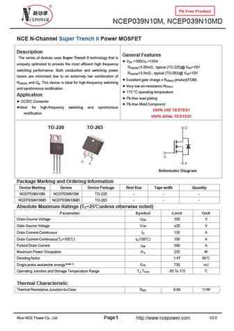
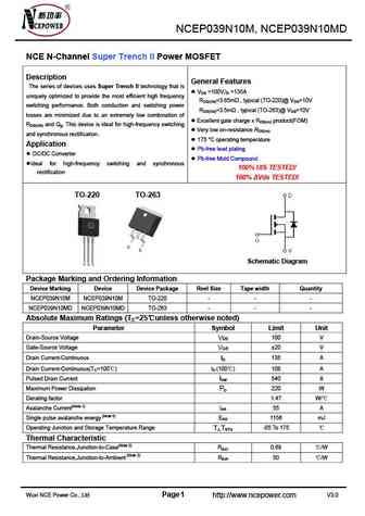
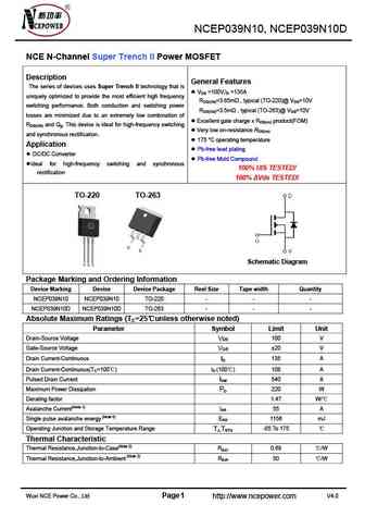
Pb Free Product NCEP039N10M, NCEP039N10MD NCE N-Channel Super Trench II Power MOSFET Description General Features The series of devices uses Super Trench II technology that is V =100V,I =135A DS D uniquely optimized to provide the most efficient high frequency R =3.65m , typical (TO-220)@ V =10V DS(ON) GS switching performance. Both conduction and switching power R =3.5m , t
8.2. Size:1810K ncepower
ncep039n10d.pdf 

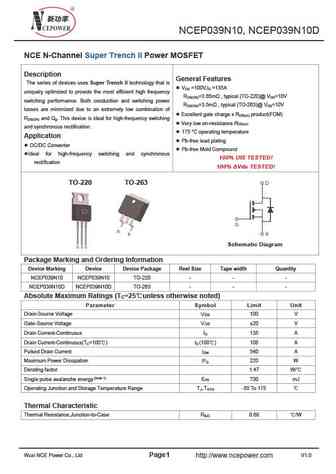
NCEP039N10, NCEP039N10D NCE N-Channel Super Trench II Power MOSFET Description General Features The series of devices uses Super Trench II technology that is V =100V,I =135A DS D uniquely optimized to provide the most efficient high frequency R =3.65m , typical (TO-220)@ V =10V DS(ON) GS switching performance. Both conduction and switching power R =3.5m , typical (TO-263)@ V
8.3. Size:679K ncepower
ncep036n10msl.pdf 

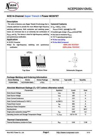
NCEP036N10MSL NCE N-Channel Super Trench II Power MOSFET Description The series of devices uses Super Trench II technology that is General Features uniquely optimized to provide the most efficient high frequency V =100V,I =215A DS D switching performance. Both conduction and switching power R =3.0m , typical@ V =10V DS(ON) GS losses are minimized due to an extremely low combinat
8.4. Size:1386K ncepower
ncep035n60ag.pdf 

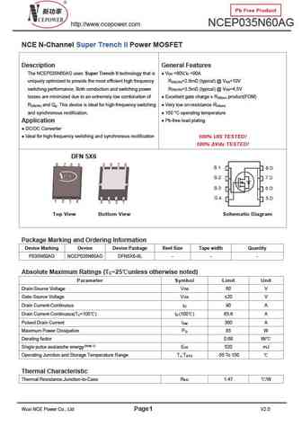
Pb Free Product http //www.ncepower.com NCEP035N60AG NCE N-Channel Super Trench II Power MOSFET Description General Features The NCEP035N60AG uses Super Trench II technology that is V =60V,I =90A DS D uniquely optimized to provide the most efficient high frequency R =2.8m (typical) @ V =10V DS(ON) GS switching performance. Both conduction and switching power R =3.5m (typical) @
8.5. Size:397K ncepower
ncep035n10m.pdf 

NCEP035N10M, NCEP035N10MD NCE N-Channel Super Trench II Power MOSFET Description General Features The series of devices uses Super Trench II technology that is VDS =100V,ID =150A uniquely optimized to provide the most efficient high frequency RDS(ON)=3.0m , typical (TO-220)@ VGS=10V switching performance. Both conduction and switching power RDS(ON)=2.8m , typical (TO
8.6. Size:931K ncepower
ncep030n60agu.pdf 

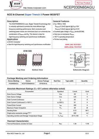
Pb Free Product http //www.ncepower.com NCEP030N60AGU NCE N-Channel Super Trench II Power MOSFET Description General Features The NCEP030N60AGU uses Super Trench II technology that V =60V,I =95A DS D is uniquely optimized to provide the most efficient high R =2.2m (typical) @ V =10V DS(ON) GS frequency switching performance. Both conduction and R =3.0m (typical) @ V =4.5V DS(ON
8.7. Size:314K ncepower
ncep039n10f.pdf 

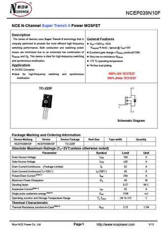
NCEP039N10F NCE N-Channel Super Trench II Power MOSFET Description The series of devices uses Super Trench II technology that is General Features uniquely optimized to provide the most efficient high frequency VDS =100V,ID =62A switching performance. Both conduction and switching power RDS(ON)=4.4m , typical @ VGS=10V losses are minimized due to an extremely low combinati
8.8. Size:1095K ncepower
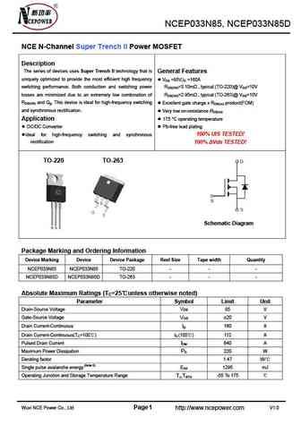
ncep033n85d.pdf 

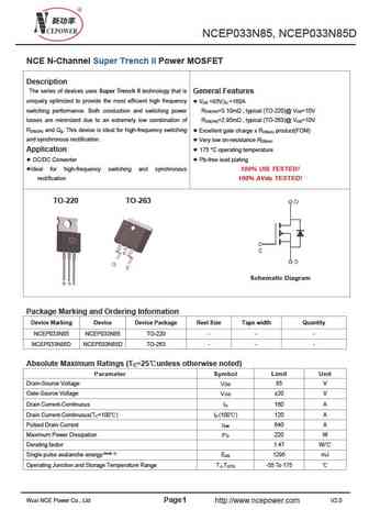
NCEP033N85, NCEP033N85D NCE N-Channel Super Trench II Power MOSFET Description The series of devices uses Super Trench II technology that is General Features uniquely optimized to provide the most efficient high frequency V =85V,I =160A DS D switching performance. Both conduction and switching power R =3.10m , typical (TO-220)@ V =10V DS(ON) GS losses are minimized due to an ext
8.9. Size:500K ncepower
ncep030n12.pdf 

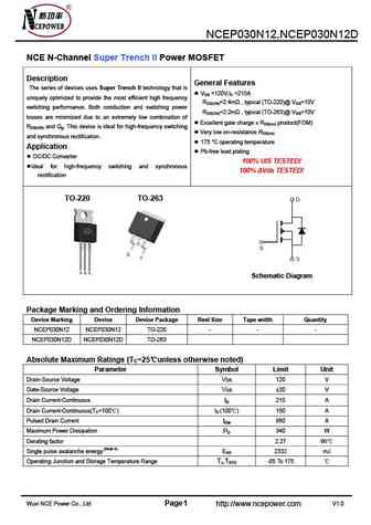
NCEP030N12,NCEP030N12D NCE N-Channel Super Trench II Power MOSFET Description General Features The series of devices uses Super Trench II technology that is VDS =120V,ID =215A uniquely optimized to provide the most efficient high frequency RDS(ON)=2.4m , typical (TO-220)@ VGS=10V switching performance. Both conduction and switching power RDS(ON)=2.2m , typical (TO-26
8.10. Size:758K ncepower
ncep030n85gu.pdf 

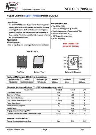
http //www.ncepower.com NCEP030N85GU NCE N-Channel Super Trench II Power MOSFET Description General Features The NCEP030N85GU uses Super Trench II technology that is V =85V,I =140A DS D uniquely optimized to provide the most efficient high frequency R =2.65m (typical) @ V =10V DS(ON) GS switching performance. Both conduction and switching power Excellent gate charge x R pro
8.11. Size:414K ncepower
ncep035n85 ncep035n85d.pdf 

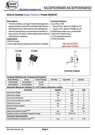
NCEP035N85,NCEP035N85D http //www.ncepower.com NCE N-Channel Super Trench II Power MOSFET Description General Features The series of devices uses Super Trench II technology that is VDS =85V,ID =150A uniquely optimized to provide the most efficient high frequency RDS(ON)=3.3m , typical (TO-220)@ VGS=10V switching performance. Both conduction and switching power RDS(ON)=3.1m
8.12. Size:402K ncepower
ncep033n10.pdf 

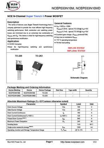
NCEP033N10, NCEP033N10D NCE N-Channel Super Trench II Power MOSFET Description General Features The series of devices uses Super Trench II technology that is VDS =100V,ID =160A uniquely optimized to provide the most efficient high frequency RDS(ON)=2.9m , typical (TO-220)@ VGS=10V switching performance. Both conduction and switching power RDS(ON)=2.7m , typical (TO-2
8.13. Size:1515K ncepower
ncep039n10md.pdf 

Pb Free Product NCEP039N10M, NCEP039N10MD NCE N-Channel Super Trench II Power MOSFET Description General Features The series of devices uses Super Trench II technology that is V =100V,I =135A DS D uniquely optimized to provide the most efficient high frequency R =3.65m , typical (TO-220)@ V =10V DS(ON) GS switching performance. Both conduction and switching power R =3.5m , t
8.14. Size:729K ncepower
ncep035n60k.pdf 

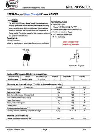
http //www.ncepower.com NCEP035N60K NCE N-Channel Super Trench II Power MOSFET Description General Features The NCEP035N60K uses Super Trench II technology that is V =60V,I =130A DS D uniquely optimized to provide the most efficient high frequency R =2.8m (typical) @ V =10V DS(ON) GS switching performance. Both conduction and switching power Excellent gate charge x R produc
8.15. Size:717K ncepower
ncep035n60ak.pdf 

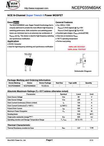
http //www.ncepower.com NCEP035N60AK NCE N-Channel Super Trench II Power MOSFET Description General Features The NCEP035N60AK uses Super Trench II technology that is V =60V,I =130A DS D uniquely optimized to provide the most efficient high frequency R =2.8m (typical) @ V =10V DS(ON) GS switching performance. Both conduction and switching power R =3.5m (typical) @ V =4.5V DS(ON)
8.16. Size:414K ncepower
ncep035n85d.pdf 

NCEP035N85,NCEP035N85D http //www.ncepower.com NCE N-Channel Super Trench II Power MOSFET Description General Features The series of devices uses Super Trench II technology that is VDS =85V,ID =150A uniquely optimized to provide the most efficient high frequency RDS(ON)=3.3m , typical (TO-220)@ VGS=10V switching performance. Both conduction and switching power RDS(ON)=3.1m
8.17. Size:500K ncepower
ncep030n12 ncep030n12d.pdf 

NCEP030N12,NCEP030N12D NCE N-Channel Super Trench II Power MOSFET Description General Features The series of devices uses Super Trench II technology that is VDS =120V,ID =215A uniquely optimized to provide the most efficient high frequency RDS(ON)=2.4m , typical (TO-220)@ VGS=10V switching performance. Both conduction and switching power RDS(ON)=2.2m , typical (TO-26
8.18. Size:1095K ncepower
ncep033n85.pdf 

NCEP033N85, NCEP033N85D NCE N-Channel Super Trench II Power MOSFET Description The series of devices uses Super Trench II technology that is General Features uniquely optimized to provide the most efficient high frequency V =85V,I =160A DS D switching performance. Both conduction and switching power R =3.10m , typical (TO-220)@ V =10V DS(ON) GS losses are minimized due to an ext
8.19. Size:414K ncepower
ncep035n85.pdf 

NCEP035N85,NCEP035N85D http //www.ncepower.com NCE N-Channel Super Trench II Power MOSFET Description General Features The series of devices uses Super Trench II technology that is VDS =85V,ID =150A uniquely optimized to provide the most efficient high frequency RDS(ON)=3.3m , typical (TO-220)@ VGS=10V switching performance. Both conduction and switching power RDS(ON)=3.1m
8.20. Size:500K ncepower
ncep030n12d.pdf 

NCEP030N12,NCEP030N12D NCE N-Channel Super Trench II Power MOSFET Description General Features The series of devices uses Super Trench II technology that is VDS =120V,ID =215A uniquely optimized to provide the most efficient high frequency RDS(ON)=2.4m , typical (TO-220)@ VGS=10V switching performance. Both conduction and switching power RDS(ON)=2.2m , typical (TO-26
8.21. Size:338K ncepower
ncep039n10m ncep039n10md.pdf 

NCEP039N10M, NCEP039N10MD NCE N-Channel Super Trench II Power MOSFET Description General Features The series of devices uses Super Trench II technology that is VDS =100V,ID =135A uniquely optimized to provide the most efficient high frequency RDS(ON)=3.65m , typical (TO-220)@ VGS=10V switching performance. Both conduction and switching power RDS(ON)=3.5m , typical (
8.22. Size:346K ncepower
ncep035n12.pdf 

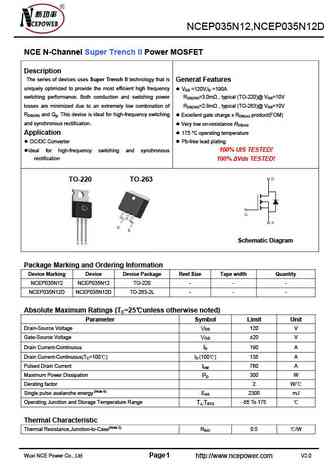
NCEP035N12,NCEP035N12D NCE N-Channel Super Trench II Power MOSFET Description The series of devices uses Super Trench II technology that is General Features uniquely optimized to provide the most efficient high frequency VDS =120V,ID =190A switching performance. Both conduction and switching power RDS(ON)=3.0m , typical (TO-220)@ VGS=10V losses are minimized due to an ext
8.23. Size:777K ncepower
ncep035n72gu.pdf 

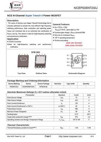
NCEP035N72GU NCE N-Channel Super Trench II Power MOSFET Description The series of devices uses Super Trench II technology that is General Features uniquely optimized to provide the most efficient high frequency V =72V,I =120A DS D switching performance. Both conduction and switching power R =2.4m , typical @ V =10V DS(ON) GS losses are minimized due to an extremely low combinat
8.24. Size:309K ncepower
ncep035n12vd.pdf 

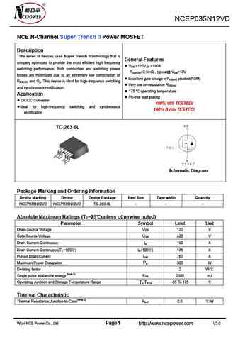
NCEP035N12VD NCE N-Channel Super Trench II Power MOSFET Description The series of devices uses Super Trench II technology that is General Features uniquely optimized to provide the most efficient high frequency VDS =120V,ID =190A switching performance. Both conduction and switching power RDS(ON)=2.5m , typical@ VGS=10V losses are minimized due to an extremely low combin
8.25. Size:346K ncepower
ncep035n12d.pdf 

NCEP035N12,NCEP035N12D NCE N-Channel Super Trench II Power MOSFET Description The series of devices uses Super Trench II technology that is General Features uniquely optimized to provide the most efficient high frequency VDS =120V,ID =190A switching performance. Both conduction and switching power RDS(ON)=3.0m , typical (TO-220)@ VGS=10V losses are minimized due to an ext
8.26. Size:346K ncepower
ncep035n12 ncep035n12d.pdf 

NCEP035N12,NCEP035N12D NCE N-Channel Super Trench II Power MOSFET Description The series of devices uses Super Trench II technology that is General Features uniquely optimized to provide the most efficient high frequency VDS =120V,ID =190A switching performance. Both conduction and switching power RDS(ON)=3.0m , typical (TO-220)@ VGS=10V losses are minimized due to an ext
8.27. Size:402K ncepower
ncep033n10m.pdf 

NCEP033N10M, NCEP033N10MD NCE N-Channel Super Trench II Power MOSFET Description General Features The series of devices uses Super Trench II technology that is VDS =100V,ID =160A uniquely optimized to provide the most efficient high frequency RDS(ON)=2.9m , typical (TO-220)@ VGS=10V switching performance. Both conduction and switching power RDS(ON)=2.7m , typical (TO
8.28. Size:402K ncepower
ncep033n10d.pdf 

NCEP033N10, NCEP033N10D NCE N-Channel Super Trench II Power MOSFET Description General Features The series of devices uses Super Trench II technology that is VDS =100V,ID =160A uniquely optimized to provide the most efficient high frequency RDS(ON)=2.9m , typical (TO-220)@ VGS=10V switching performance. Both conduction and switching power RDS(ON)=2.7m , typical (TO-2
8.29. Size:701K ncepower
ncep033n85m.pdf 

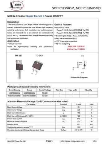
NCEP033N85M, NCEP033N85MD NCE N-Channel Super Trench II Power MOSFET Description The series of devices uses Super Trench II technology that is General Features uniquely optimized to provide the most efficient high frequency V =85V,I =160A DS D switching performance. Both conduction and switching power R =3.10m , typical (TO-220)@ V =10V DS(ON) GS losses are minimized due to an e
8.30. Size:402K ncepower
ncep033n10 ncep033n10d.pdf 

NCEP033N10, NCEP033N10D NCE N-Channel Super Trench II Power MOSFET Description General Features The series of devices uses Super Trench II technology that is VDS =100V,ID =160A uniquely optimized to provide the most efficient high frequency RDS(ON)=2.9m , typical (TO-220)@ VGS=10V switching performance. Both conduction and switching power RDS(ON)=2.7m , typical (TO-2
8.31. Size:1810K ncepower
ncep039n10.pdf 

NCEP039N10, NCEP039N10D NCE N-Channel Super Trench II Power MOSFET Description General Features The series of devices uses Super Trench II technology that is V =100V,I =135A DS D uniquely optimized to provide the most efficient high frequency R =3.65m , typical (TO-220)@ V =10V DS(ON) GS switching performance. Both conduction and switching power R =3.5m , typical (TO-263)@ V
8.32. Size:361K ncepower
ncep035n72.pdf 

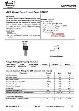
NCEP035N72 NCE N-Channel Super Trench II Power MOSFET Description The series of devices uses Super Trench II technology that is General Features uniquely optimized to provide the most efficient high frequency VDS =72V,ID =140A switching performance. Both conduction and switching power RDS(ON)=3.3m , typical @ VGS=10V losses are minimized due to an extremely low combinat
8.33. Size:992K ncepower
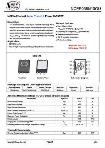
ncep038n10gu.pdf 

http //www.ncepower.com NCEP038N10GU NCE N-Channel Super Trench II Power MOSFET Description General Features The NCEP038N10GU uses Super Trench II technology that is V =100V,I =135A DS D uniquely optimized to provide the most efficient high frequency R =3.45m (Typ.) @ V =10V DS(ON) GS switching performance. Both conduction and switching power Excellent gate charge x R produ
8.34. Size:815K ncepower
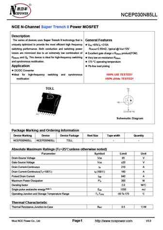
ncep030n85ll.pdf 

NCEP030N85LL NCE N-Channel Super Trench II Power MOSFET Description The series of devices uses Super Trench II technology that is General Features uniquely optimized to provide the most efficient high frequency V =85V,I =210A DS D switching performance. Both conduction and switching power R =2.65m , typical @ V =10V DS(ON) GS losses are minimized due to an extremely low combinat
8.35. Size:716K ncepower
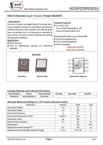
ncep030n30gu.pdf 

http //www.ncepower.com NCEP030N30GU NCE N-Channel Super Trench II Power MOSFET Description General Features The series of devices uses Super Trench II technology that is V =30V,I =65A DS D uniquely optimized to provide the most efficient high frequency R =2.65m (typical) @ V =10V DS(ON) GS switching performance. Both conduction and switching power R =4m (typical) @ V =4.5V
8.36. Size:332K ncepower
ncep033n85 ncep033n85d.pdf 

NCEP033N85, NCEP033N85D NCE N-Channel Super Trench II Power MOSFET Description The series of devices uses Super Trench II technology that is General Features uniquely optimized to provide the most efficient high frequency VDS =85V,ID =160A switching performance. Both conduction and switching power RDS(ON)=3.10m , typical (TO-220)@ VGS=10V losses are minimized due to an ex
8.37. Size:338K ncepower
ncep039n10 ncep039n10d.pdf 

NCEP039N10, NCEP039N10D NCE N-Channel Super Trench II Power MOSFET Description General Features The series of devices uses Super Trench II technology that is VDS =100V,ID =135A uniquely optimized to provide the most efficient high frequency RDS(ON)=3.65m , typical (TO-220)@ VGS=10V switching performance. Both conduction and switching power RDS(ON)=3.5m , typical (TO
8.38. Size:326K ncepower
ncep035n85gu.pdf 

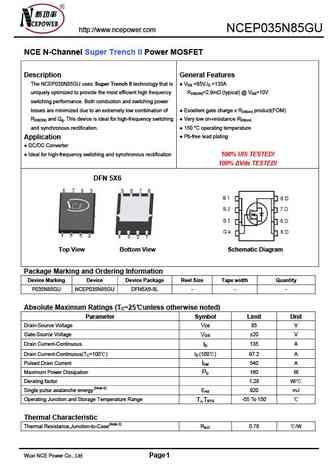
http //www.ncepower.com NCEP035N85GU NCE N-Channel Super Trench II Power MOSFET Description General Features The NCEP035N85GU uses Super Trench II technology that is VDS =85V,ID =135A uniquely optimized to provide the most efficient high frequency RDS(ON)=2.9m (typical) @ VGS=10V switching performance. Both conduction and switching power losses are minimized due to an extremel
Другие IGBT... NCEP02T11D, NCEP02T11T, NCEP030N12, NCEP030N12D, NCEP030N30GU, NCEP030N60AGU, NCEP030N85GU, NCEP030N85LL, 13N50, NCEP033N10, NCEP033N10D, NCEP033N10M, NCEP033N85M, NCEP035N10M, NCEP035N12, NCEP035N12D, NCEP035N12VD
