NCEP058N85M datasheet, аналоги, основные параметры
Наименование производителя: NCEP058N85M
Тип транзистора: MOSFET
Полярность: N
Предельные значения
Pd ⓘ - Максимальная рассеиваемая мощность: 125 W
|Vds|ⓘ - Максимально допустимое напряжение сток-исток: 85 V
|Vgs|ⓘ - Максимально допустимое напряжение затвор-исток: 20 V
|Id| ⓘ - Максимально допустимый постоянный ток стока: 95 A
Tj ⓘ - Максимальная температура канала: 175 °C
Электрические характеристики
tr ⓘ - Время нарастания: 12 ns
Cossⓘ - Выходная емкость: 540 pf
RDSonⓘ - Сопротивление сток-исток открытого транзистора: 0.0058 Ohm
Тип корпуса: TO-220
Аналог (замена) для NCEP058N85M
- подборⓘ MOSFET транзистора по параметрам
NCEP058N85M даташит
ncep058n85m.pdf
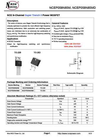
NCEP058N85M, NCEP058N85MD NCE N-Channel Super Trench II Power MOSFET Description The series of devices uses Super Trench II technology that is General Features uniquely optimized to provide the most efficient high frequency V =85V,I =95A DS D switching performance. Both conduction and switching power R =5.4m , typical (TO-220)@ V =10V DS(ON) GS losses are minimized due to an ext
ncep058n85.pdf

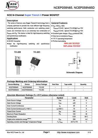
NCEP058N85, NCEP058N85D NCE N-Channel Super Trench II Power MOSFET Description The series of devices uses Super Trench II technology that is General Features uniquely optimized to provide the most efficient high frequency VDS =85V,ID =95A switching performance. Both conduction and switching power RDS(ON)=5.4m , typical (TO-220)@ VGS=10V losses are minimized due to an extr
ncep058n85gu.pdf
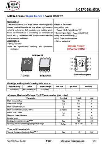
NCEP058N85GU NCE N-Channel Super Trench II Power MOSFET Description The series of devices uses Super Trench II technology that is General Features uniquely optimized to provide the most efficient high frequency VDS =85V,ID =90A switching performance. Both conduction and switching power RDS(ON)=4.8m , typical@ VGS=10V losses are minimized due to an extremely low combinatio
ncep058n85d.pdf

NCEP058N85, NCEP058N85D NCE N-Channel Super Trench II Power MOSFET Description The series of devices uses Super Trench II technology that is General Features uniquely optimized to provide the most efficient high frequency VDS =85V,ID =95A switching performance. Both conduction and switching power RDS(ON)=5.4m , typical (TO-220)@ VGS=10V losses are minimized due to an extr
Другие IGBT... NCEP055N10U, NCEP055N12, NCEP055N12AG, NCEP055N12D, NCEP055N12G, NCEP055N30GU, NCEP055N60GU, NCEP058N85GU, IRFP460, NCEP060N10, NCEP060N10D, NCEP060N10F, NCEP060N10G, NCEP060N60G, NCEP063N10AGU, NCEP063N10GU, NCEP063N85G
🌐 : EN ES РУ

Список транзисторов
Обновления
MOSFET: RM50P30DF | CRTT095N12N | CRSS028N10N | CRST030N10N | CRJQ80N65F | ASDM20N20KQ | ASDM20N100Q | ASDM12N65F | ASDM100R750PKQ | ASDM100R160NKQ | ASDM100R090NP | ASDM100R066NQ | ASDM100R045NQ | ASDM100N34KQ | ASDM100N15KQ | FTF30P35D
Popular searches
irf640 | irf840 | irf740 | c945 transistor | irf640n | 2n3904 | bc547 datasheet | k3797 mosfet