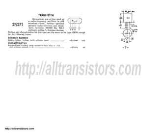
2N37 datasheet, аналоги, основные параметры
Наименование производителя: 2N37 📄📄
Тип материала: Ge
Полярность: PNP
Предельные значения
Максимальная рассеиваемая мощность (Pc): 0.05 W
Макcимально допустимое напряжение коллектор-база (Ucb): 20 V
Макcимально допустимое напряжение коллектор-эмиттер (Uce): 20 V
Макcимальный постоянный ток коллектора (Ic): 0.008 A
Предельная температура PN-перехода (Tj): 50 °C
Электрические характеристики
Граничная частота коэффициента передачи тока (ft): 0.4 MHz
Статический коэффициент передачи тока (hFE): 15
Корпус транзистора: TO22
📄📄 Копировать
Аналоги (замена) для 2N37
- подборⓘ биполярного транзистора по параметрам
2N37 даташит
2n3791 2n3792.pdf
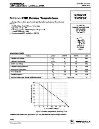
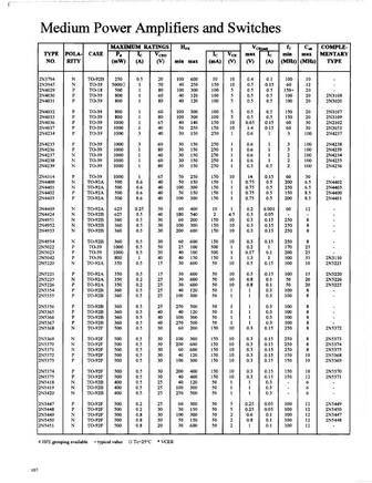
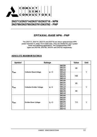
Order this document MOTOROLA by 2N3791/D SEMICONDUCTOR TECHNICAL DATA 2N3791 Silicon PNP Power Transistors 2N3792 . . . designed for medium speed switching and amplifier applications. These devices feature 10 AMPERE Total Switching Time @ 3.0 A [ 1.0 s (typ) POWER TRANSISTORS hFE (min) = 50 @ 1.0 A PNP SILICON Low VCE(sat) = 0.5 V (typ) @ IC = 5.0 A, IB = 0.5 A 60
2n3771re.pdf
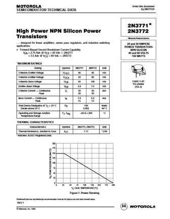
Order this document MOTOROLA by 2N3771/D SEMICONDUCTOR TECHNICAL DATA * 2N3771 High Power NPN Silicon Power 2N3772 Transistors *Motorola Preferred Device . . . designed for linear amplifiers, series pass regulators, and inductive switching 20 and 30 AMPERE applications. POWER TRANSISTORS Forward Biased Second Breakdown Current Capability NPN SILICON IS/b = 3.75 Adc @ VCE = 4
2n3715 2n3716.pdf
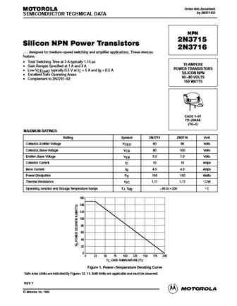
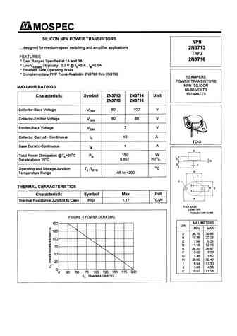
Order this document MOTOROLA by 2N3715/D SEMICONDUCTOR TECHNICAL DATA NPN 2N3715 Silicon NPN Power Transistors 2N3716 . . . designed for medium speed switching and amplifier applications. These devices feature Total Switching Time at 3 A typically 1.15 s 10 AMPERE Gain Ranges Specified at 1 A and 3 A POWER TRANSISTORS Low VCE(sat) typically 0.5 V at IC = 5 A and
2n3773 2n6609.pdf
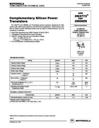
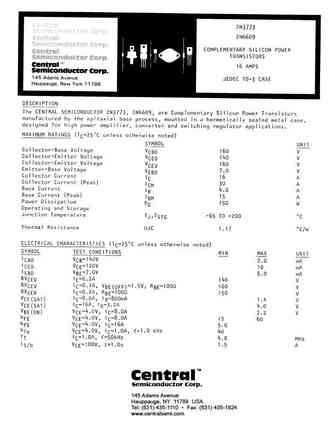
Order this document MOTOROLA by 2N3773/D SEMICONDUCTOR TECHNICAL DATA NPN 2N3773* Complementary Silicon Power PNP 2N6609 Transistors The 2N3773 and 2N6609 are PowerBase power transistors designed for high *Motorola Preferred Device power audio, disk head positioners and other linear applications. These devices can also be used in power switching circuits such as relay or solenoid d
2n3771.pdf
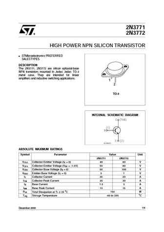
2N3771 2N3772 HIGH POWER NPN SILICON TRANSISTOR STMicroelectronics PREFERRED SALESTYPES DESCRIPTION The 2N3771, 2N3772 are silicon epitaxial-base NPN transistors mounted in Jedec Jedec TO-3 metal case. They are intended for linear amplifiers and inductive switching applications. 1 2 TO-3 INTERNAL SCHEMATIC DIAGRAM ABSOLUTE MAXIMUM RATINGS Symbol Parameter Value Unit 2N3771
2n3771 2n3772.pdf

2N3771 2N3772 HIGH POWER NPN SILICON TRANSISTOR STMicroelectronics PREFERRED SALESTYPES DESCRIPTION The 2N3771, 2N3772 are silicon epitaxial-base NPN transistors mounted in Jedec Jedec TO-3 metal case. They are intended for linear amplifiers and inductive switching applications. 1 2 TO-3 INTERNAL SCHEMATIC DIAGRAM ABSOLUTE MAXIMUM RATINGS Symbol Parameter Value Unit 2N3771
2n3700hr.pdf
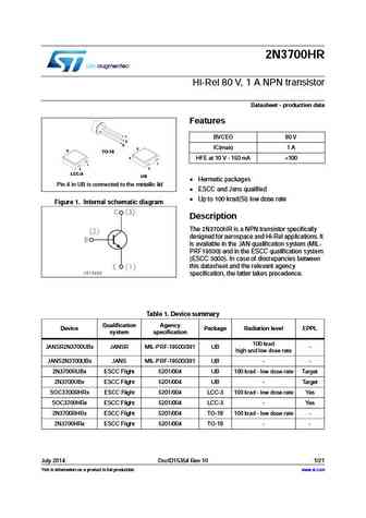
2N3700HR Hi-Rel 80 V, 1 A NPN transistor Datasheet - production data Features 1 BVCEO 80 V 2 3 IC(max) 1 A 3 3 TO-18 4 HFE at 10 V - 150 mA >100 1 1 2 2 LCC-3 UB Hermetic packages Pin 4 in UB is connected to the metallic lid ESCC and Jans qualified Up to 100 krad(Si) low dose rate Figure 1. Internal schematic diagram Description The 2N3700HR is a NPN tr
2n3773.pdf
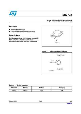
2N3773 High power NPN transistor Features High power dissipation Low collector-emitter saturation voltage Description The device is a planar NPN transistor mounted in 1 TO-3 metal case. It is intended for linear 2 amplifiers and inductive switching applications. TO-3 Figure 1. Internal schematic diagram Table 1. Device summary Order code Marking Package Packaging 2N3773
2n3700.pdf
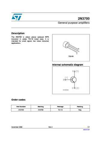
2N3700 General purpose amplifiers Description The 2N3700 is silicon planar epitaxial NPN transistor in Jedec TO-18 metal case. It is intended for small signal, low noise industrial applications. TO-18 Internal schematic diagram Order codes Part Number Marking Package Packing 2N3700 2N3700 TO-18 Bag November 2006 Rev 2 1/7 www.st.com 7 Electrical ratings 2N3700 1 Electrical ratin
2n3703.pdf
2N3703 PNP General Purpose Amplifier This device designed for use as general purpose amplifier and switches requiring collector currents to 300mA. Sourced from Process 66. TO-92 1 1. Emitter 2. Collector 3. Base PNP Epitaxial Silicon Transistor Absolute Maximum Ratings* Ta=25 C unless otherwise noted Symbol Parameter Value Units VCEO Collector-Emitter Voltage -30 V VCBO
2n3702.pdf
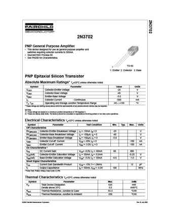
2N3702 PNP General Purpose Amplifier This device designed for use as general purpose amplifier and switches requiring collector currents to 300mA. Sourced from Process 68. See PN200 for Characteristics. TO-92 1 1. Emitter 2. Collector 3. Base PNP Epitaxial Silicon Transistor Absolute Maximum Ratings* Ta=25 C unless otherwise noted Symbol Parameter Value Units VCEO Co
2n3704.pdf

2N3704 NPN General Purpose Amplifier This device designed for use as general purpose amplifier and switches requiring collector currents to 300mA. Sourced from Process 10. See PN100 for characteristics. TO-92 1 1. Emitter 2. Collector 3. Base NPN Epitaxial Silicon Transistor Absolute Maximum Ratings* Ta=25 C unless otherwise noted Symbol Parameter Value Units VCEO Co
2n3724 2n3725-a.pdf
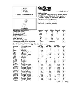
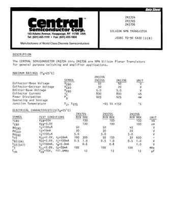
2N3724 2N3725 www.centralsemi.com 2N3725A DESCRIPTION NPN SILICON TRANSISTOR The CENTRAL SEMICONDUCTOR 2N3724, 2N3725, 2N3725A types are Silicon NPN Planar Epitaxial Transistors designed for high voltage, high current, high speed switching applications. MARKING FULL PART NUMBER TO-39 CASE MAXIMUM RATINGS (TA=25 C) SYMBOL 2N3724 2N3725 2N3725A UNITS Collector-Base Voltage VCB
2n3726 2n3727.pdf
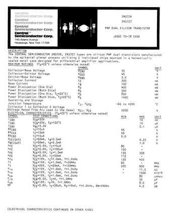
TM Central Semiconductor Corp. 145 Adams Avenue Hauppauge, NY 11788 USA Tel (631) 435-1110 Fax (631) 435-1824 www.centralsemi.com
2n3707 2n3708 2n3709 2n3710 2n3711.pdf
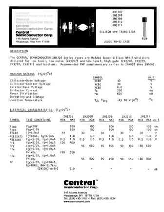
TM Central Semiconductor Corp. 145 Adams Avenue Hauppauge, NY 11788 USA Tel (631) 435-1110 Fax (631) 435-1824 www.centralsemi.com
2n3789 2n3790 2n3791 2n3792.pdf
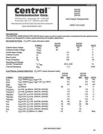
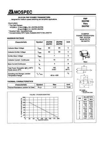
DATA SHEET 2N3789 2N3790 2N3791 2N3792 PNP POWER TRANSISTORS JEDEC TO-3 CASE DESCRIPTION The CENTRAL SEMICONDUCTOR 2N3789 Series types are silicon power transistors manufactured by the epitaxial planar process and designed for medium speed switching and amplifier applications. MAXIMUM RATINGS (TC=25 C unless otherwise noted) 2N3789 2N3790 SYMBOL 2N3791 2N3792 UNITS Col
2n3713 2n3714 2n3715 2n3716.pdf
145 Adams Avenue, Hauppauge, NY 11788 USA Tel (631) 435-1110 Fax (631) 435-1824
2n3700 2n3701.pdf
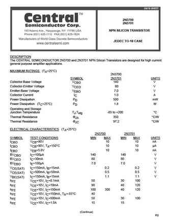
DATA SHEET 2N3700 2N3701 NPN SILICON TRANSISTOR JEDEC TO-18 CASE DESCRIPTION The CENTRAL SEMICONDUCTOR 2N3700 and 2N3701 NPN Silicon Transistors are designed for high current general purpose amplifier applications. MAXIMUM RATINGS (TA=25 C) 2N3700 SYMBOL 2N3701 UNITS Collector-Base Voltage VCBO 140 V Collector-Emitter Voltage VCEO 80 V Emitter-Base Voltage VEBO 7.0 V
2n3773 2n6609.pdf
TM Central Semiconductor Corp. 145 Adams Avenue Hauppauge, NY 11788 USA Tel (631) 435-1110 Fax (631) 435-1824 www.centralsemi.com
2n3704 2n3705 2n3706.pdf
145 Adams Avenue, Hauppauge, NY 11788 USA Tel (631) 435-1110 Fax (631) 435-1824
2n3773g.pdf
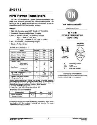
2N3773 NPN Power Transistors The 2N3773 is a PowerBaset power transistor designed for high power audio, disk head positioners and other linear applications. This device can also be used in power switching circuits such as relay or solenoid drivers, DC-DC converters or inverters. http //onsemi.com Features High Safe Operating Area (100% Tested) 150 W @ 100 V 16 A NPN Completely
2n3771 2n3772.pdf
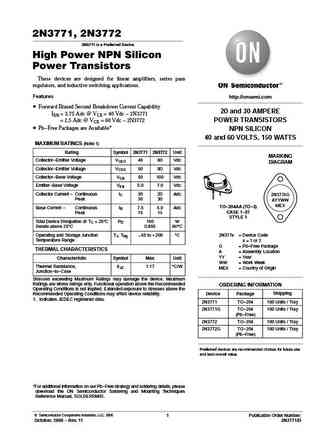
2N3771, 2N3772 2N3771 is a Preferred Device High Power NPN Silicon Power Transistors These devices are designed for linear amplifiers, series pass regulators, and inductive switching applications. Features http //onsemi.com Forward Biased Second Breakdown Current Capability 20 and 30 AMPERE IS/b = 3.75 Adc @ VCE = 40 Vdc - 2N3771 = 2.5 Adc @ VCE = 60 Vdc - 2N3772 POWER TRANSISTO
2n3771g.pdf

2N3771, 2N3772 2N3771 is a Preferred Device High Power NPN Silicon Power Transistors These devices are designed for linear amplifiers, series pass regulators, and inductive switching applications. Features http //onsemi.com Forward Biased Second Breakdown Current Capability 20 and 30 AMPERE IS/b = 3.75 Adc @ VCE = 40 Vdc - 2N3771 = 2.5 Adc @ VCE = 60 Vdc - 2N3772 POWER TRANSISTO
2n3772g.pdf

2N3771, 2N3772 2N3771 is a Preferred Device High Power NPN Silicon Power Transistors These devices are designed for linear amplifiers, series pass regulators, and inductive switching applications. Features http //onsemi.com Forward Biased Second Breakdown Current Capability 20 and 30 AMPERE IS/b = 3.75 Adc @ VCE = 40 Vdc - 2N3771 = 2.5 Adc @ VCE = 60 Vdc - 2N3772 POWER TRANSISTO
2n3773 2n6609.pdf
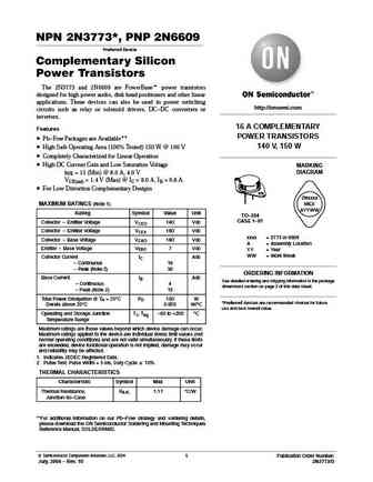
NPN 2N3773*, PNP 2N6609 Preferred Device Complementary Silicon Power Transistors The 2N3773 and 2N6609 are PowerBaset power transistors designed for high power audio, disk head positioners and other linear applications. These devices can also be used in power switching http //onsemi.com circuits such as relay or solenoid drivers, DC-DC converters or inverters. 16 A COMPLEMENTARY Feat
2n3772.pdf
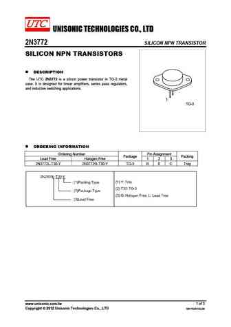
UNISONIC TECHNOLOGIES CO., LTD 2N3772 SILICON NPN TRANSISTOR SILICON NPN TRANSISTORS DESCRIPTION The UTC 2N3772 is a silicon power transistor in TO-3 metal case. It is designed for linear amplifiers, series pass regulators, and inductive switching applications. 1 TO-3 ORDERING INFORMATION Ordering Number Pin Assignment Package Packing Lead Free Halogen Free 1 2 3 2N3
2n3773.pdf
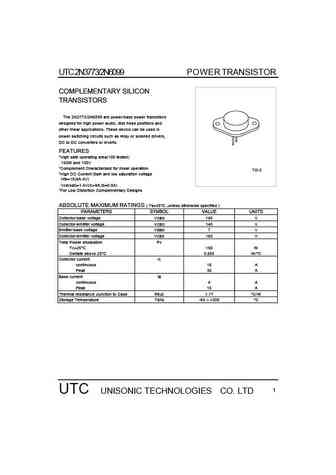
UTC 2N3773/2N6099 P O W E R TRANSISTOR COMPLEMENTARY SILICON TRANSISTORS The 2N3773/2N6099 are power-base power transistors designed for high power audio, disk head positions and other linear applications. These device can be used in power switching circuits such as relay or solened drivers, DC to DC converters or inverts. FEATURES *High safe operating area(100 tested) 150W and 100V
2n3713-2n3714-2n3715-2n3716-2n3789-2n3790-2n3791-2n3792.pdf
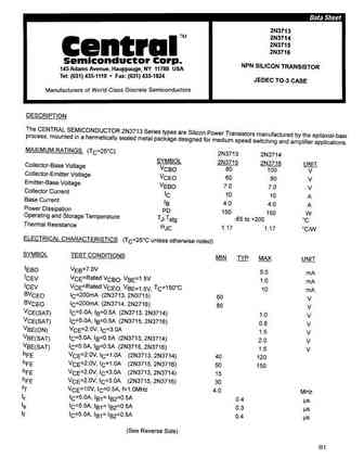
2N3713/2N3714/2N3715/2N3716 - NPN 2N3789/2N3790/2N3791/2N3792 - PNP EPITAXIAL-BASE NPN - PNP The 2N3713, 2N3714, 2N3715 and 2N3716 are silicon epitaxial-base NPN power transistor in Jedec TO-3 metal case. They are inteded for use in power linear and switching applications. The complementary PNP types are 2N3789, 2N3790, 2N3791 and 2N3792 respectively. ABSOLUTE MAXIMUM RATINGS Symbol Rat
2n3724l.pdf

INCH-POUND The documentation and process conversion measures necessary to comply with this document shall be MIL-PRF-19500/728C completed by 25 January 2011. 25 October 2010 MIL-PRF-19500/728B SUPERSEDING 16 December 2007 PERFORMANCE SPECIFICATION SHEET * SEMICONDUCTOR DEVICE, TRANSISTOR, NPN, SILICON, SWITCHING, TYPES 2N3724, 2N3724L, 2N3724UB, 2N3725, 2N3725L, 2N3725UB,
2n3725ub.pdf

INCH-POUND The documentation and process conversion measures necessary to comply with this document shall be MIL-PRF-19500/728C completed by 25 January 2011. 25 October 2010 MIL-PRF-19500/728B SUPERSEDING 16 December 2007 PERFORMANCE SPECIFICATION SHEET * SEMICONDUCTOR DEVICE, TRANSISTOR, NPN, SILICON, SWITCHING, TYPES 2N3724, 2N3724L, 2N3724UB, 2N3725, 2N3725L, 2N3725UB,
2n3724ub.pdf
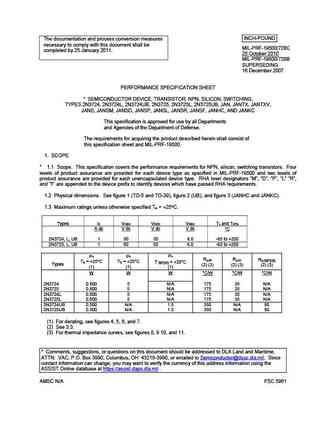
INCH-POUND The documentation and process conversion measures necessary to comply with this document shall be MIL-PRF-19500/728C completed by 25 January 2011. 25 October 2010 MIL-PRF-19500/728B SUPERSEDING 16 December 2007 PERFORMANCE SPECIFICATION SHEET * SEMICONDUCTOR DEVICE, TRANSISTOR, NPN, SILICON, SWITCHING, TYPES 2N3724, 2N3724L, 2N3724UB, 2N3725, 2N3725L, 2N3725UB,
2n3768.pdf
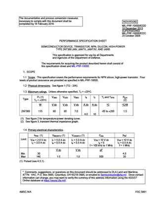
The documentation and process conversion measures necessary to comply with this document shall be INCH-POUND completed by 18 February 2014. MIL-PRF-19500/622D 18 December 2013 SUPERSEDING MIL-PRF-19500/622C 25 October 2008 PERFORMANCE SPECIFICATION SHEET SEMICONDUCTOR DEVICE, TRANSISTOR, NPN, SILICON, HIGH-POWER TYPE 2N7368 JAN, JANTX, JANTXV, AND JANS This specification
2n3725l.pdf

INCH-POUND The documentation and process conversion measures necessary to comply with this document shall be MIL-PRF-19500/728C completed by 25 January 2011. 25 October 2010 MIL-PRF-19500/728B SUPERSEDING 16 December 2007 PERFORMANCE SPECIFICATION SHEET * SEMICONDUCTOR DEVICE, TRANSISTOR, NPN, SILICON, SWITCHING, TYPES 2N3724, 2N3724L, 2N3724UB, 2N3725, 2N3725L, 2N3725UB,
2n3716x.pdf
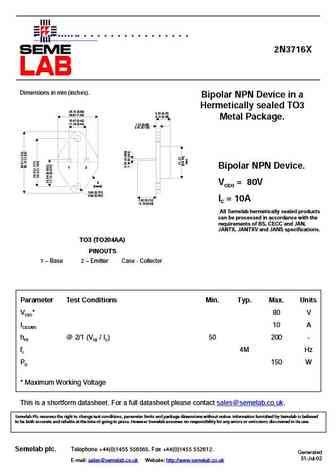
"2N3716X" 2N3716X Dimensions in mm (inches). Bipolar NPN Device in a Hermetically sealed TO3 25.15 (0.99) 6.35 (0.25) 26.67 (1.05) 9.15 (0.36) Metal Package. 10.67 (0.42) 11.18 (0.44) 1.52 (0.06) 3.43 (0.135) 1 2 Bipolar NPN Device. 3 VCEO = 80V (case) 3.84 (0.151) 4.09 (0.161) 7.92 (0.312) IC = 10A 12.70 (0.50) All Semelab hermetically sealed produ
2n3799.pdf
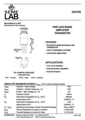
2N3799 SEME LAB MECHANICAL DATA Dimensions in mm (inches) PNP, LOW NOISE 5.84 (0.230) 5.31 (0.209) AMPLIFIER 4.95 (0.195) 4.52 (0.178) TRANSISTOR FEATURES SILICON PLANAR EPITAXIAL PNP TRANSISTOR 0.48 (0.019) 0.41 (0.016) CECC SCREENING OPTIONS dia. LOW NOISE AMPLIFIER 2.54 (0.100) Nom. APPLICATIONS 3 1 Low Level Amplifier 2 Instrumentation Amplifier
2n3714smd.pdf

2N3714SMD Dimensions in mm (inches). Bipolar NPN Device in a Hermetically sealed 0.89 (0.035) min. Ceramic Surface Mount 3.70 (0.146) 3.70 (0.146) 3.60 (0.142) 3.41 (0.134) 3.41 (0.134) Max. Package for High Reliability Applications 1 3 Bipolar NPN Device. 2 VCEO = 80V IC = 10A 9.67 (0.381) All Semelab hermetically sealed products 9.38 (0.369) 0.50 (0.020) 0.26 (
2n3790smd.pdf

2N3790SMD Dimensions in mm (inches). Bipolar PNP Device in a Hermetically sealed 0.89 (0.035) min. Ceramic Surface Mount 3.70 (0.146) 3.70 (0.146) 3.60 (0.142) 3.41 (0.134) 3.41 (0.134) Max. Package for High Reliability Applications 1 3 Bipolar PNP Device. 2 VCEO = 80V IC = 10A 9.67 (0.381) All Semelab hermetically sealed products 9.38 (0.369) 0.50 (0.020) 0.26 (
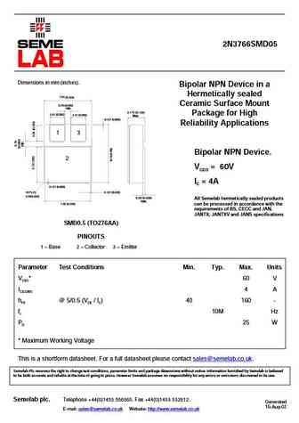
2n3766smd.pdf

2N3766SMD Dimensions in mm (inches). Bipolar NPN Device in a Hermetically sealed 0.89 (0.035) min. Ceramic Surface Mount 3.70 (0.146) 3.70 (0.146) 3.60 (0.142) 3.41 (0.134) 3.41 (0.134) Max. Package for High Reliability Applications 1 3 Bipolar NPN Device. 2 VCEO = 60V IC = 4A 9.67 (0.381) All Semelab hermetically sealed products 9.38 (0.369) 0.50 (0.020) 0.26 (0
2n3738.pdf
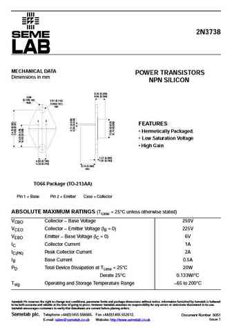
2N3738 MECHANICAL DATA POWER TRANSISTORS Dimensions in mm NPN SILICON 6.35 (0.250) 8.64 (0.340) 3.68 (0.145) rad. 3.61 (0.142) max. 4.08(0.161) rad. 1 2 FEATURES Hermetically Packaged. Low Saturation Voltage High Gain 1.27 (0.050) 1.91 (0.750) 4.83 (0.190) 5.33 (0.210) 9.14 (0.360) min. TO66 Package (TO-213AA) Pin 1 = Base Pin 2 = Emitter Case = Collector A
2n3715x.pdf

2N3715X Dimensions in mm (inches). Bipolar NPN Device in a Hermetically sealed TO3 25.15 (0.99) 6.35 (0.25) 26.67 (1.05) 9.15 (0.36) Metal Package. 10.67 (0.42) 11.18 (0.44) 1.52 (0.06) 3.43 (0.135) 1 2 Bipolar NPN Device. 3 VCEO = 60V (case) 3.84 (0.151) 4.09 (0.161) 7.92 (0.312) IC = 10A 12.70 (0.50) All Semelab hermetically sealed products can be processed in
2n3713smd.pdf

2N3713SMD Dimensions in mm (inches). Bipolar NPN Device in a Hermetically sealed 0.89 (0.035) min. Ceramic Surface Mount 3.70 (0.146) 3.70 (0.146) 3.60 (0.142) 3.41 (0.134) 3.41 (0.134) Max. Package for High Reliability Applications 1 3 Bipolar NPN Device. 2 VCEO = 60V IC = 10A 9.67 (0.381) All Semelab hermetically sealed products 9.38 (0.369) 0.50 (0.020) 0.26 (
2n3735csm4.pdf
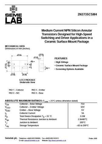
2N3735CSM4 Medium Current NPN Silicon Annular Transistors Designed for High-Speed Switching and Driver Applications in a Ceramic Surface Mount Package MECHANICAL DATA Dimensions in mm (inches) 1.40 0.15 5.59 0.13 (0.055 0.006) (0.22 0.005) 0.25 0.03 (0.01 0.001) FEATURES 0.23 rad. (0.009) High Voltage 3 2 Ceramic Surface Mount Package 0.23 4 1 min
2n3734.pdf
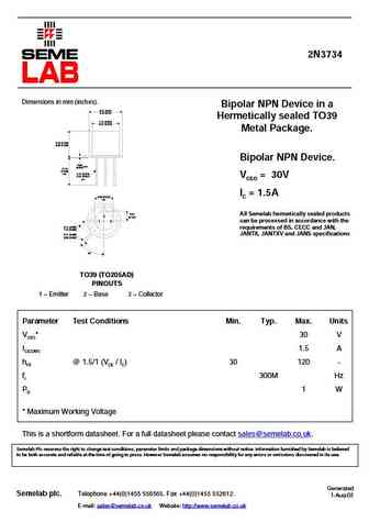
2N3734 Dimensions in mm (inches). Bipolar NPN Device in a 8.51 (0.34) 9.40 (0.37) Hermetically sealed TO39 7.75 (0.305) 8.51 (0.335) Metal Package. 6.10 (0.240) 6.60 (0.260) Bipolar NPN Device. 0.89 max. (0.035) 12.70 (0.500) min. 0.41 (0.016) 0.53 (0.021) VCEO = 30V dia. IC = 1.5A 5.08 (0.200) typ. 2.54 All Semelab hermetically sealed products 2 (0.100) 1
2n3789xsmd.pdf

2N3789XSMD Dimensions in mm (inches). Bipolar PNP Device in a Hermetically sealed 0.89 (0.035) min. Ceramic Surface Mount 3.70 (0.146) 3.70 (0.146) 3.60 (0.142) 3.41 (0.134) 3.41 (0.134) Max. Package for High Reliability Applications 1 3 Bipolar PNP Device. 2 VCEO = 60V IC = 10A 9.67 (0.381) All Semelab hermetically sealed products 9.38 (0.369) 0.50 (0.020) 0.26
2n3767smd05.pdf
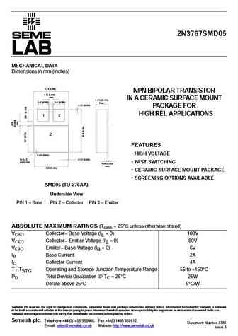
2N3767SMD05 MECHANICAL DATA Dimensions in mm (inches) 7.54 (0.296) NPN BIPOLAR TRANSISTOR 0.76 (0.030) min. IN A CERAMIC SURFACE MOUNT 3.175 (0.125) 2.41 (0.095) 2.41 (0.095) Max. 0.127 (0.005) PACKAGE FOR HIGH REL APPLICATIONS 1 3 2 FEATURES HIGH VOLTAGE 0.127 (0.005) 16 PLCS 0.127 (0.005) 0.50(0.020) FAST SWITCHING 0.50 (0.020) max. 7.26 (0.286) CER
2n3740r.pdf
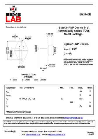
2N3740R Dimensions in mm (inches). Bipolar PNP Device in a Hermetically sealed TO66 6.35 (0.250) Metal Package. 8.64 (0.340) 3.68 (0.145) rad. 3.61 (0.142) max. 4.08(0.161) rad. Bipolar PNP Device. 1 2 VCEO = 60V IC = 4A All Semelab hermetically sealed products can be processed in accordance with the requirements of BS, CECC and JAN, JANTX, JANTXV and JANS speci
2n3789x.pdf
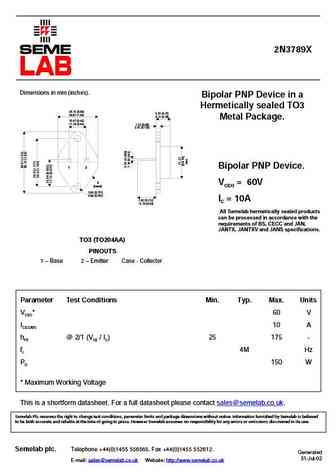
2N3789X Dimensions in mm (inches). Bipolar PNP Device in a Hermetically sealed TO3 25.15 (0.99) 6.35 (0.25) 26.67 (1.05) 9.15 (0.36) Metal Package. 10.67 (0.42) 11.18 (0.44) 1.52 (0.06) 3.43 (0.135) 1 2 Bipolar PNP Device. 3 VCEO = 60V (case) 3.84 (0.151) 4.09 (0.161) 7.92 (0.312) IC = 10A 12.70 (0.50) All Semelab hermetically sealed products can be processed in
2n3724.pdf

2N3724 Dimensions in mm (inches). Bipolar NPN Device in a 8.51 (0.34) 9.40 (0.37) Hermetically sealed TO39 7.75 (0.305) 8.51 (0.335) Metal Package. 6.10 (0.240) 6.60 (0.260) Bipolar NPN Device. 0.89 max. (0.035) 12.70 (0.500) min. 0.41 (0.016) 0.53 (0.021) VCEO = 30V dia. IC = 0.5A 5.08 (0.200) typ. 2.54 All Semelab hermetically sealed products 2 (0.100) 1
2n3716smd.pdf

2N3716SMD Dimensions in mm (inches). Bipolar NPN Device in a Hermetically sealed 0.89 (0.035) min. Ceramic Surface Mount 3.70 (0.146) 3.70 (0.146) 3.60 (0.142) 3.41 (0.134) 3.41 (0.134) Max. Package for High Reliability Applications 1 3 Bipolar NPN Device. 2 VCEO = 80V IC = 10A 9.67 (0.381) All Semelab hermetically sealed products 9.38 (0.369) 0.50 (0.020) 0.26 (
2n3790xsmd.pdf

2N3790XSMD Dimensions in mm (inches). Bipolar PNP Device in a Hermetically sealed 0.89 (0.035) min. Ceramic Surface Mount 3.70 (0.146) 3.70 (0.146) 3.60 (0.142) 3.41 (0.134) 3.41 (0.134) Max. Package for High Reliability Applications 1 3 Bipolar PNP Device. 2 VCEO = 80V IC = 10A 9.67 (0.381) All Semelab hermetically sealed products 9.38 (0.369) 0.50 (0.020) 0.26
2n3792smd.pdf

2N3792SMD Dimensions in mm (inches). Bipolar PNP Device in a Hermetically sealed 0.89 (0.035) min. Ceramic Surface Mount 3.70 (0.146) 3.70 (0.146) 3.60 (0.142) 3.41 (0.134) 3.41 (0.134) Max. Package for High Reliability Applications 1 3 Bipolar PNP Device. 2 VCEO = 80V IC = 10A 9.67 (0.381) All Semelab hermetically sealed products 9.38 (0.369) 0.50 (0.020) 0.26 (
2n3715smd.pdf

2N3715SMD Dimensions in mm (inches). Bipolar NPN Device in a Hermetically sealed 0.89 (0.035) min. Ceramic Surface Mount 3.70 (0.146) 3.70 (0.146) 3.60 (0.142) 3.41 (0.134) 3.41 (0.134) Max. Package for High Reliability Applications 1 3 Bipolar NPN Device. 2 VCEO = 60V IC = 10A 9.67 (0.381) All Semelab hermetically sealed products 9.38 (0.369) 0.50 (0.020) 0.26 (
2n3767smd.pdf
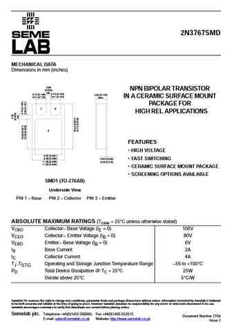
2N3767SMD MECHANICAL DATA Dimensions in mm (inches) NPN BIPOLAR TRANSISTOR IN A CERAMIC SURFACE MOUNT PACKAGE FOR HIGH REL APPLICATIONS FEATURES HIGH VOLTAGE FAST SWITCHING CERAMIC SURFACE
2n3791smd.pdf
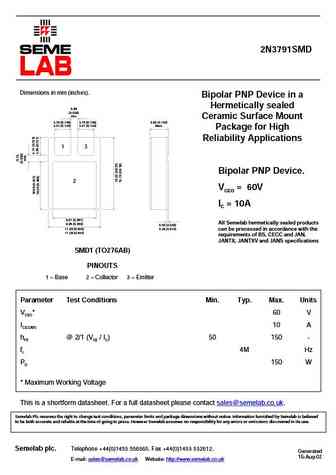
2N3791SMD Dimensions in mm (inches). Bipolar PNP Device in a Hermetically sealed 0.89 (0.035) min. Ceramic Surface Mount 3.70 (0.146) 3.70 (0.146) 3.60 (0.142) 3.41 (0.134) 3.41 (0.134) Max. Package for High Reliability Applications 1 3 Bipolar PNP Device. 2 VCEO = 60V IC = 10A 9.67 (0.381) All Semelab hermetically sealed products 9.38 (0.369) 0.50 (0.020) 0.26 (
2n3766smd05.pdf
2N3766SMD05 Dimensions in mm (inches). Bipolar NPN Device in a Hermetically sealed 7.54 (0.296) 0.76 (0.030) Ceramic Surface Mount min. 3.175 (0.125) 2.41 (0.095) Package for High 2.41 (0.095) Max. 0.127 (0.005) Reliability Applications 1 3 Bipolar NPN Device. 2 VCEO = 60V IC = 4A 0.127 (0.005) 16 PLCS 0.127 (0.005) 0.50(0.020) 0.50 (0.020) All Semelab herm
2n3741smd.pdf
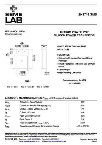
2N3741 SMD SEME LAB MECHANICAL DATA MEDIUM POWER PNP Dimensions in mm SILICON POWER TRANSISTOR LOW SATURATION VOLTAGE HIGH GAIN FEATURES Hermetically sealed Surface Mount Package. Small Footprint - efficient use of PCB space. Lightweight
2n3724a.pdf
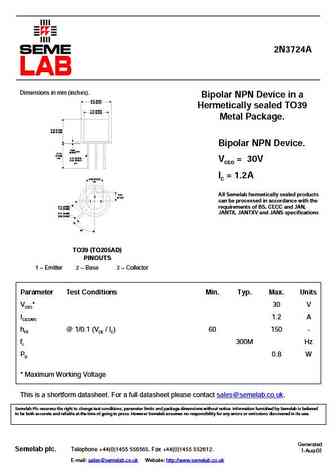
2N3724A Dimensions in mm (inches). Bipolar NPN Device in a 8.51 (0.34) 9.40 (0.37) Hermetically sealed TO39 7.75 (0.305) 8.51 (0.335) Metal Package. 6.10 (0.240) 6.60 (0.260) Bipolar NPN Device. 0.89 max. (0.035) 12.70 (0.500) min. 0.41 (0.016) 0.53 (0.021) VCEO = 30V dia. IC = 1.2A 5.08 (0.200) typ. 2.54 All Semelab hermetically sealed products 2 (0.100) 1
2n3772.pdf
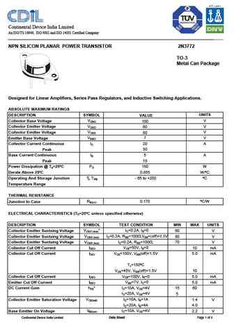
Continental Device India Limited An ISO/TS 16949, ISO 9001 and ISO 14001 Certified Company 2N3772 NPN SILICON PLANAR POWER TRANSISTOR TO-3 Metal Can Package Designed for Linear Amplifiers, Series Pass Regulators, and Inductive Switching Applications. ABSOLUTE MAXIMUM RATINGS DESCRIPTION SYMBOL UNITS VALUE Collector Base Voltage VCBO V 100 Collector Emitter Voltage VCEO V 60 Colle
2n3702 03.pdf
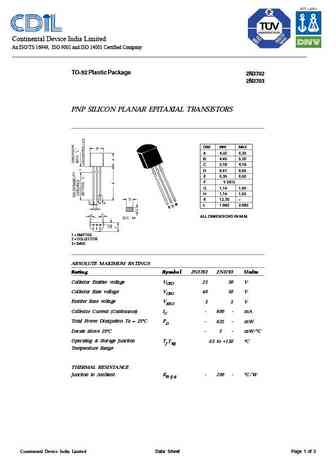
Continental Device India Limited An ISO/TS 16949, ISO 9001 and ISO 14001 Certified Company TO-92 Plastic Package 2N3702 2N3703 PNP SILICON PLANAR EPITAXIAL TRANSISTORS DIM MIN MAX A 4,32 5,33 B 4,45 5,20 C 3,18 4,19 D 0,41 0,55 E 0,35 0,50 F 5 DEG G 1,14 1,40 H 1,14 1,53 K 12,70 L 1.982 2.082 ALL DIMENSIONS IN M.M. 1 2 3 1 = EMITTER 2 = COLLECTOR 3 = BASE ABSOLUTE MAXI
2n3704 05.pdf
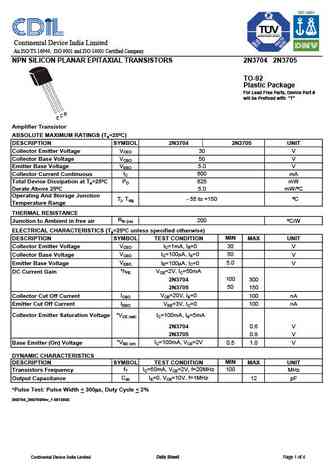
Continental Device India Limited An ISO/TS 16949, ISO 9001 and ISO 14001 Certified Company NPN SILICON PLANAR EPITAXIAL TRANSISTORS 2N3704 2N3705 TO-92 Plastic Package For Lead Free Parts, Device Part # will be Prefixed with "T" B C E Amplifier Transistor ABSOLUTE MAXIMUM RATINGS (Ta=25 C) DESCRIPTION SYMBOL 2N3704 2N3705 UNIT VCEO Collector Emitter Voltage 30 V Collector Base
2n3700 01.pdf
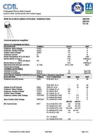
Continental Device India Limited An ISO/TS 16949, ISO 9001 and ISO 14001 Certified Company NPN SILICON PLANAR EPITAXIAL TRANSISTORS 2N3700 2N3701 TO-18 General purpose amplifier ABSOLUTE MAXIMUM RATINGS. DESCRIPTION SYMBOL VALUE UNIT Collector -Base Voltage VCBO 140 V Collector -Emitter Voltage VCEO 80 V Emitter -Base Voltage VEBO 7.0 V Collector Current IC 1.0 A Power Dissipation @
2n3773.pdf
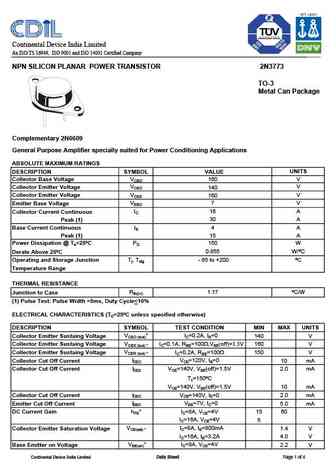
Continental Device India Limited An ISO/TS 16949, ISO 9001 and ISO 14001 Certified Company 2N3773 NPN SILICON PLANAR POWER TRANSISTOR TO-3 Metal Can Package Complementary 2N6609 General Purpose Amplifier specially suited for Power Conditioning Applications ABSOLUTE MAXIMUM RATINGS DESCRIPTION SYMBOL UNITS VALUE Collector Base Voltage VCBO 160 V Collector Emitter Voltage VCEO V 140
2n3773.pdf
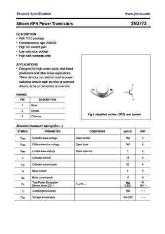
Product Specification www.jmnic.com Silicon NPN Power Transistors 2N3773 DESCRIPTION With TO-3 package Complement to type 2N6609 High DC current gain Low saturation voltage High safe operating area APPLICATIONS Designed for high power audio, disk head positioners and other linear applications. These devices can also be used in power switching circuits such as
2n3749 2n2880.pdf
TECHNICAL DATA PNP POWER SILICON TRANSISTOR Qualified per MIL-PRF-19500/315 Devices Qualified Level JAN 2N2880 2N3749 JANTX JANTXV MAXIMUM RATINGS Ratings Symbol Value Units Collector-Emitter Voltage 80 Vdc VCEO Collector-Base Voltage 110 Vdc VCBO Emitter-Base Voltage 8.0 Vdc VEBO Base Current I 0.5 Adc B Collector Current 5.0 Adc IC Total Power Dissipation
2n3735l.pdf
TECHNICAL DATA SHEET 6 Lake Street, Lawrence, MA 01841 1-800-446-1158 / (978) 620-2600 / Fax (978) 689-0803 Website http //www.microsemi.com NPN SILICON SWITCHING TRANSISTOR Qualified per MIL-PRF-19500/395 DEVICES LEVELS 2N3735 2N3735L JAN 2N3737 2N3737UB JANTX JANTXV JANS ABSOLUTE MAXIMUM RATINGS (TC = +25 C unless otherwise noted) Parameters / Test Conditions Symbol M
2n3740a.pdf
7516 Central Industrial Drive Riviera Beach, Florida 33404 PHONE (561) 842-0305 FAX (561) 845-7813 2N3740A APPLICATIONS Drivers Switches Medium-Power Amplifiers FEATURES Medium Power Low Saturation Voltage 0.6 VCE(sat) @ IC = 1.0 Amp High Gain Characteristics hFE @ IC = 250 mA 30-100 PNP Transistors Excellent Safe Area Limits Low Collector Cuto
2n3019 2n3057 2n3700.pdf
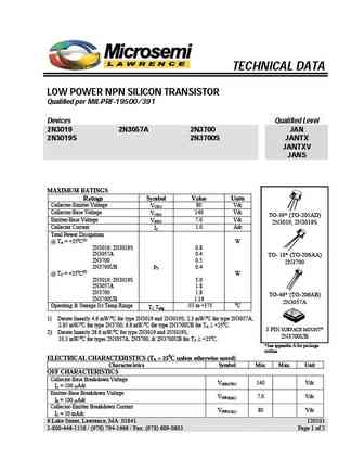
TECHNICAL DATA LOW POWER NPN SILICON TRANSISTOR Qualified per MIL-PRF-19500/391 Devices Qualified Level 2N3019 2N3057A 2N3700 JAN 2N3019S 2N3700S JANTX JANTXV JANS MAXIMUM RATINGS Ratings Symbol Value Units Collector-Emitter Voltage 80 Vdc VCEO Collector-Base Voltage 140 Vdc VCBO TO-39* (TO-205AD) Emitter-Base Voltage 7.0 Vdc VEBO 2N3019, 2N3019S Collector
2n3741a.pdf

7516 Central Industrial Drive Riviera Beach, Florida 33404 PHONE (561) 842-0305 FAX (561) 845-7813 2N3741A APPLICATIONS Drivers Switches Medium-Power Amplifiers FEATURES Medium Power Low Saturation Voltage 0.6 VCE(sat) @ IC = 1.0 Amp High Gain Characteristics hFE @ IC = 250 mA 30-100 PNP Transistors Excellent Safe Area Limits Low Collector Cuto
2n3737ub.pdf

TECHNICAL DATA SHEET 6 Lake Street, Lawrence, MA 01841 1-800-446-1158 / (978) 620-2600 / Fax (978) 689-0803 Website http //www.microsemi.com NPN SILICON SWITCHING TRANSISTOR Qualified per MIL-PRF-19500/395 DEVICES LEVELS 2N3735 2N3735L JAN 2N3737 2N3737UB JANTX JANTXV JANS ABSOLUTE MAXIMUM RATINGS (TC = +25 C unless otherwise noted) Parameters / Test Conditions Symbol M
2n3763l.pdf

TECHNICAL DATA PNP SWITCHING SILICON TRANSISTOR Qualified per MIL-PRF-19500/396 Devices Qualified Level JAN 2N3762 2N3763 2N3764 2N3765 JANTX 2N3762L 2N3763L JANTXV MAXIMUM RATINGS 2N3762* 2N3763* Ratings Symbol Unit 2N3764 2N3765 Collector-Emitter Voltage 40 60 Vdc VCEO Collector-Base Voltage 40 60 Vdc VCBO TO-39* (TO-205AD) Emitter-Base Voltage 5.0 Vdc VE
2n3719.pdf

7516 Central Industrial Drive Riviera Beach, Florida 33404 PHONE (561) 842-0305 FAX (561) 845-7813 2N3719 APPLICATIONS High-Speed Switching Medium-Current Switching High-Frequency Amplifiers FEATURES Collector-Emitter Sustaining Voltage Silicon PNP VCEO(SUS) = 40 Vdc (Min) - 2N3719 Power Transistors DC Current Gain hFE = 25-180 @ IC = 1.0 Adc Low Co
2n3743 2n4930 2n4931.pdf
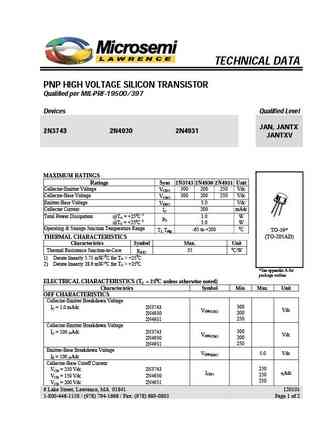
TECHNICAL DATA PNP HIGH VOLTAGE SILICON TRANSISTOR Qualified per MIL-PRF-19500/397 Devices Qualified Level JAN, JANTX 2N3743 2N4930 2N4931 JANTXV MAXIMUM RATINGS Ratings Sym 2N3743 2N4930 2N4931 Unit Collector-Emitter Voltage 300 200 250 Vdc VCEO Collector-Base Voltage 300 200 250 Vdc VCBO Emitter-Base Voltage 5.0 Vdc VEBO Collector Current 200 mAdc IC Total
2n3740.pdf
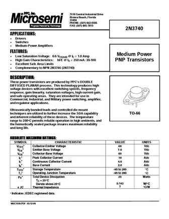
7516 Central Industrial Drive Riviera Beach, Florida 33404 PHONE (561) 842-0305 FAX (561) 845-7813 2N3740 APPLICATIONS Drivers Switches Medium-Power Amplifiers FEATURES Medium Power Low Saturation Voltage 0.6 VCE(sat) @ IC = 1.0 Amp High Gain Characteristics hFE @ IC = 250 mA 30-100 PNP Transistors Excellent Safe Area Limits Complementary to NP
2n3762 2n3763 2n3764 2n3765.pdf
TECHNICAL DATA PNP SWITCHING SILICON TRANSISTOR Qualified per MIL-PRF-19500/396 Devices Qualified Level JAN 2N3762 2N3763 2N3764 2N3765 JANTX 2N3762L 2N3763L JANTXV MAXIMUM RATINGS 2N3762* 2N3763* Ratings Symbol Unit 2N3764 2N3765 Collector-Emitter Voltage 40 60 Vdc VCEO Collector-Base Voltage 40 60 Vdc VCBO TO-39* (TO-205AD) Emitter-Base Voltage 5.0 Vdc VE
2n3720.pdf
7516 Central Industrial Drive Riviera Beach, Florida 33404 PHONE (561) 842-0305 FAX (561) 845-7813 2N3720 APPLICATIONS High-Speed Switching Medium-Current Switching High-Frequency Amplifiers FEATURES Collector-Emitter Sustaining Voltage Silicon PNP VCEO(SUS) = 60 Vdc (Min) - 2N3720 Power Transistors DC Current Gain hFE = 25-180 @ IC = 1.0 Adc Low Co
2n3762l.pdf

TECHNICAL DATA PNP SWITCHING SILICON TRANSISTOR Qualified per MIL-PRF-19500/396 Devices Qualified Level JAN 2N3762 2N3763 2N3764 2N3765 JANTX 2N3762L 2N3763L JANTXV MAXIMUM RATINGS 2N3762* 2N3763* Ratings Symbol Unit 2N3764 2N3765 Collector-Emitter Voltage 40 60 Vdc VCEO Collector-Base Voltage 40 60 Vdc VCBO TO-39* (TO-205AD) Emitter-Base Voltage 5.0 Vdc VE
2n3741.pdf

7516 Central Industrial Drive Riviera Beach, Florida 33404 PHONE (561) 842-0305 FAX (561) 845-7813 2N3741 APPLICATIONS Drivers Switches Medium-Power Amplifiers FEATURES Medium Power Low Saturation Voltage 0.6 VCE(sat) @ IC = 1.0 Amp High Gain Characteristics hFE @ IC = 250 mA 30-100 PNP Transistors Excellent Safe Area Limits Complementary to NP
2n3737.pdf
2N3737 Silicon NPN Transistor Data Sheet Description Applications General purpose Low power Semicoa Semiconductors offers NPN silicon transistor Screening and processing per MIL-PRF-19500 Appendix E JAN level (2N3737J) JANTX level (2N3737JX) JANTXV level (2N3737JV) JANS level (2N3737JS) QCI to the applicable level 100% die visual
2n3715 2n3716.pdf
NPN Power Silicon Transistor 2N3715 & 2N3716 Features Available in JAN, JANTX, and JANTXV per MIL-PRF-19500/408 TO-3 (TO-204AA) Package Maximum Ratings Ratings Symbol 2N3715 2N3716 Units Collector - Emitter Voltage VCEO 60 80 Vdc Collector - Base Voltage VCBO 80 100 Vdc Emitter - Base Voltage VEBO 7.0 Vdc Base Current IB 4.0 Adc Collector Current IC 10 Adc Total Power Diss
2n3766 2n3767.pdf
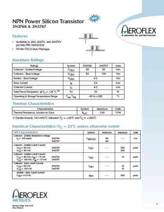
NPN Power Silicon Transistor 2N3766 & 2N3767 Features Available in JAN, JANTX, and JANTXV per MIL-PRF-19500/518 TO-66 (TO-213AA) Package Maximum Ratings Ratings Symbol 2N3766 2N3767 Units Collector - Emitter Voltage VCEO 60 80 Vdc Collector - Base Voltage VCBO 80 100 Vdc Emitter - Base Voltage VEBO 6.0 Vdc Base Current IB 2.0 Adc Collector Current IC 4.0 Adc Total Power Di
2n3403 2n3404 2n3405 2n3414 2n3415 2n3416 2n3417 2n3702 2n3703 2n3704 2n3705 2n3706 2n3707 2n3708 2n3709 2n3710.pdf

2n3711 2n3721 2n3827 2n3858 2n3858a 2n3859 2n3859a 2n3860 2n3877 2n3877a 2n3900 2n3900a 2n3901 2n3903 2n3904 2n3905.pdf
2n3773t3bl.pdf
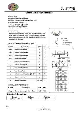
2N3773T3BL Silicon NPN Power Transistor DESCRIPTION Excellent Safe Operating Area High DC Current Gain-h =15(Min)@I = 8A FE C Low Saturation Voltage- V )= 1.4V(Max)@ I = 8A CE(sat C Complement to Type 2N6609 APPLICATIONS Designed for high power audio ,disk head positioners and other linear applications, which can also be used in power switching circuits such as relay or
2n3772.pdf
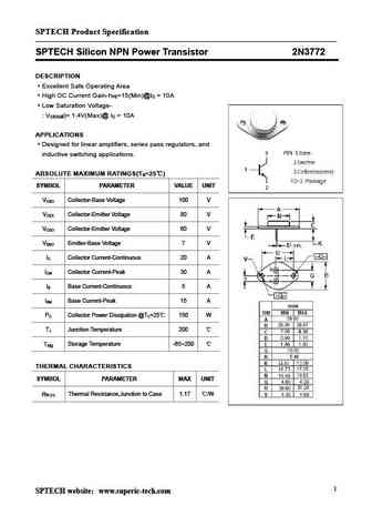
SPTECH Product Specification SPTECH Silicon NPN Power Transistor 2N3772 DESCRIPTION Excellent Safe Operating Area High DC Current Gain-h =15(Min)@I = 10A FE C Low Saturation Voltage- V )= 1.4V(Max)@ I = 10A CE(sat C APPLICATIONS Designed for linear amplifiers, series pass regulators, and inductive switching applications. ABSOLUTE MAXIMUM RATINGS(T =25 ) a SYMBOL PARAME
2n3771.pdf
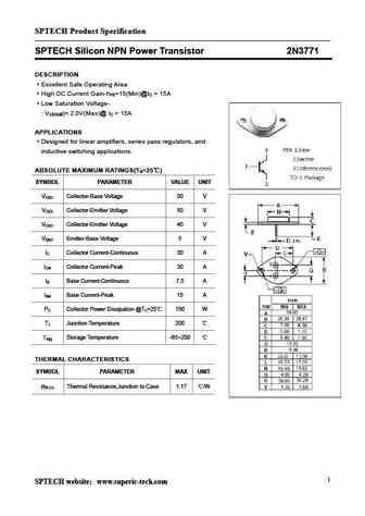
SPTECH Product Specification SPTECH Silicon NPN Power Transistor 2N3771 DESCRIPTION Excellent Safe Operating Area High DC Current Gain-h =15(Min)@I = 15A FE C Low Saturation Voltage- V )= 2.0V(Max)@ I = 15A CE(sat C APPLICATIONS Designed for linear amplifiers, series pass regulators, and inductive switching applications. ABSOLUTE MAXIMUM RATINGS(T =25 ) a SYMBOL PARAME
2n3773.pdf
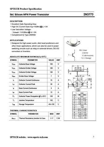
SPTECH Product Specification isc Silicon NPN Power Transistor 2N3773 DESCRIPTION Excellent Safe Operating Area High DC Current Gain-h =15(Min)@I = 8A FE C Low Saturation Voltage- V )= 1.4V(Max)@ I = 8A CE(sat C Complement to Type 2N6609 APPLICATIONS Designed for high power audio ,disk head positioners and other linear applications, which can also be used in power switch
2n3772.pdf
isc Silicon NPN Power Transistor 2N3772 DESCRIPTION Excellent Safe Operating Area High DC Current Gain-h =15(Min)@I = 10A FE C Low Saturation Voltage- V )= 1.4V(Max)@ I = 10A CE(sat C 100% avalanche tested Minimum Lot-to-Lot variations for robust device performance and reliable operation. APPLICATIONS Designed for linear amplifiers, series pass regulators, and inducti
2n3716.pdf
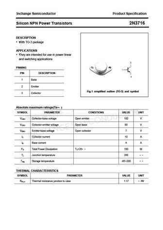
Inchange Semiconductor Product Specification Silicon NPN Power Transistors 2N3716 DESCRIPTION With TO-3 package APPLICATIONS They are intended for use in power linear and switching applications PINNING PIN DESCRIPTION 1 Base 2 Emitter Fig.1 simplified outline (TO-3) and symbol 3 Collector Absolute maximum ratings(Ta= ) SYMBOL PARAMETER CONDITIONS VALUE UNIT VCBO
2n3791 2n3792.pdf
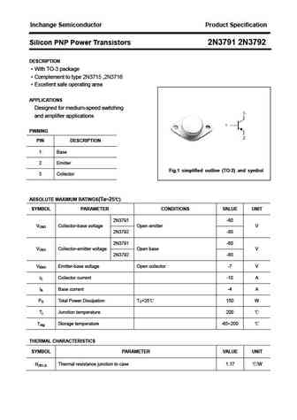
Inchange Semiconductor Product Specification Silicon PNP Power Transistors 2N3791 2N3792 DESCRIPTION With TO-3 package Complement to type 2N3715 ,2N3716 Excellent safe operating area APPLICATIONS Designed for medium-speed switching and amplifier applications PINNING PIN DESCRIPTION 1 Base 2 Emitter Fig.1 simplified outline (TO-3) and symbol 3 Collector ABSOLUTE M
2n3790.pdf
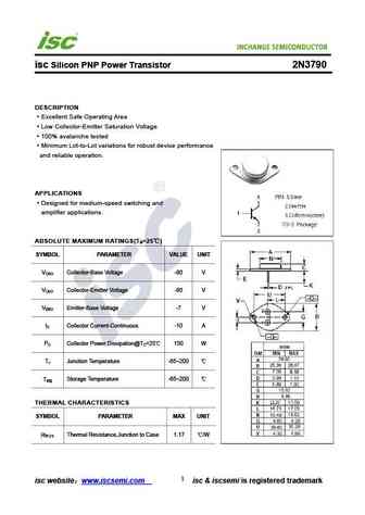
isc Silicon PNP Power Transistor 2N3790 DESCRIPTION Excellent Safe Operating Area Low Collector-Emitter Saturation Voltage 100% avalanche tested Minimum Lot-to-Lot variations for robust device performance and reliable operation. APPLICATIONS Designed for medium-speed switching and amplifier applications. ABSOLUTE MAXIMUM RATINGS(T =25 ) a SYMBOL PARAMETER VALUE UNIT V C
2n3771.pdf
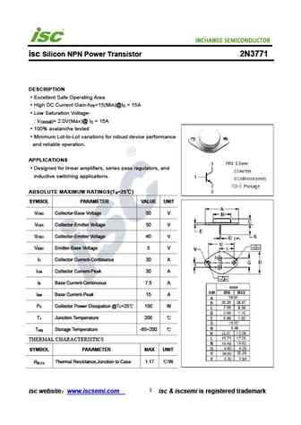
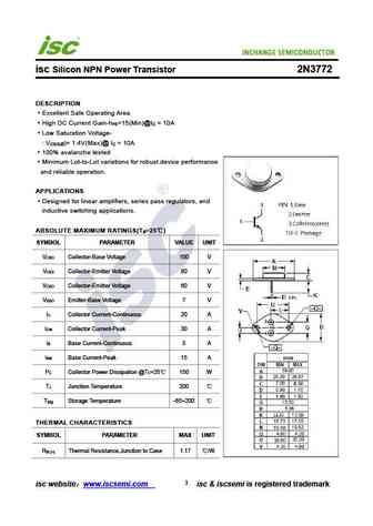
INCHANGE Semiconductor isc Silicon NPN Power Transistor 2N3771 DESCRIPTION Excellent Safe Operating Area High DC Current Gain-h =15(Min)@I = 15A FE C Low Saturation Voltage- V )= 2.0V(Max)@ I = 15A CE(sat C 100% avalanche tested Minimum Lot-to-Lot variations for robust device performance and reliable operation. APPLICATIONS Designed for linear amplifiers, series pass
2n3792.pdf

INCHANGE Semiconductor isc Silicon PNP Power Transistor 2N3792 DESCRIPTION Excellent Safe Operating Area Low Collector-Emitter Saturation Voltage 100% tested Minimum Lot-to-Lot variations for robust device performance and reliable operation. APPLICATIONS Designed for medium-speed switching and amplifier applications. ABSOLUTE MAXIMUM RATINGS(T =25 ) a SYMBOL PARAMETER V
2n3740a.pdf
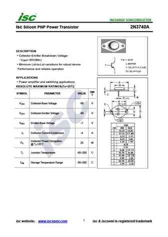
isc Silicon PNP Power Transistor 2N3740A DESCRIPTION Collector-Emitter Breakdown Voltage- V =-60V(Min) CEO Minimum Lot-to-Lot variations for robust device Performance and reliable operation APPLICATIONS Power amplifier and switching applications ABSOLUTE MAXIMUM RATINGS(Ta=25 ) UNI SYMBOL PARAMETER VALUE T V Collector-Base Voltage -60 V CBO V Collector-Emitter Voltage -
2n3715 2n3716.pdf
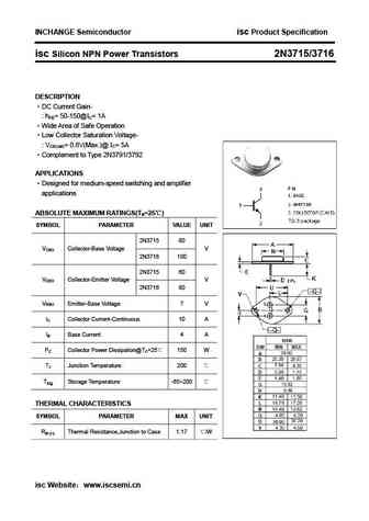
INCHANGE Semiconductor isc Product Specification isc Silicon NPN Power Transistors 2N3715/3716 DESCRIPTION DC Current Gain- hFE= 50-150@IC= 1A Wide Area of Safe Operation Low Collector Saturation Voltage- VCE(sat)= 0.8V(Max.)@ IC= 5A Complement to Type 2N3791/3792 APPLICATIONS Designed for medium-speed switching and amplifier applications ABSOLUTE MAXIMU
2n3741a.pdf

isc Silicon PNP Power Transistor 2N3741A DESCRIPTION Collector-Emitter Breakdown Voltage- V =-80V(Min) CEO Minimum Lot-to-Lot variations for robust device Performance and reliable operation APPLICATIONS Power amplifier and switching applications ABSOLUTE MAXIMUM RATINGS(Ta=25 ) UNI SYMBOL PARAMETER VALUE T V Collector-Base Voltage -80 V CBO V Collector-Emitter Voltage -
2n3773.pdf
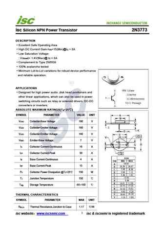
INCHANGE Semiconductor isc Silicon NPN Power Transistor 2N3773 DESCRIPTION Excellent Safe Operating Area High DC Current Gain-h =15(Min)@I = 8A FE C Low Saturation Voltage- V )= 1.4V(Max)@ I = 8A CE(sat C Complement to Type 2N6609 100% avalanche tested Minimum Lot-to-Lot variations for robust device performance and reliable operation. APPLICATIONS Designed for high
2n3714.pdf
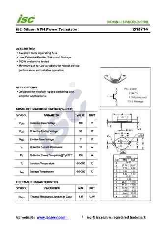
isc Silicon NPN Power Transistor 2N3714 DESCRIPTION Excellent Safe Operating Area Low Collector-Emitter Saturation Voltage 100% avalanche tested Minimum Lot-to-Lot variations for robust device performance and reliable operation. APPLICATIONS Designed for medium-speed switching and amplifier applications. ABSOLUTE MAXIMUM RATINGS(T =25 ) a SYMBOL PARAMETER VALUE UNIT V C
2n3713.pdf

isc Silicon NPN Power Transistor 2N3713 DESCRIPTION Excellent Safe Operating Area Low Collector-Emitter Saturation Voltage 100% avalanche tested Minimum Lot-to-Lot variations for robust device performance and reliable operation. APPLICATIONS Designed for medium-speed switching and amplifier applications. ABSOLUTE MAXIMUM RATINGS(T =25 ) a SYMBOL PARAMETER VALUE UNIT V C
2n3740 2n3741.pdf
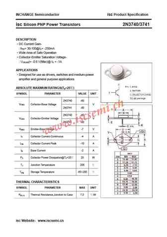
INCHANGE Semiconductor isc Product Specification isc Silicon PNP Power Transistors 2N3740/3741 DESCRIPTION DC Current Gain- hFE= 30-100@IC= -250mA Wide Area of Safe Operation Collector-Emitter Saturation Voltage- VCE(sat)= -0.6 V(Max)@ IC = -1A APPLICATIONS Designed for use as drivers, switches and medium-power amplifier and general purpose applications ABSOL
2n3772j.pdf
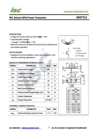
isc Silicon NPN Power Transistor 2N3772J DESCRIPTION J High DC Current Gain-h 100-150@I = 10A FE C Low Saturation Voltage- V )= 1.4V(Max)@ I = 10A CE(sat C Minimum Lot-to-Lot variations for robust device performance and reliable operation. APPLICATIONS Designed for linear amplifiers, series pass regulators, and inductive switching applications. ABSOLUTE MAXIMUM RATINGS(T
2n3789.pdf

isc Silicon PNP Power Transistor 2N3789 DESCRIPTION Excellent Safe Operating Area Low Collector-Emitter Saturation Voltage 100% avalanche tested Minimum Lot-to-Lot variations for robust device performance and reliable operation. APPLICATIONS Designed for medium-speed switching and amplifier applications. ABSOLUTE MAXIMUM RATINGS(T =25 ) a SYMBOL PARAMETER VALUE UNIT V C
Другие транзисторы: 2N3688, 2N3689, 2N369, 2N3690, 2N3691, 2N3692, 2N3693, 2N3694, 2SC5198, 2N370, 2N3700, 2N3700CSM, 2N3700DCSM, 2N3700UB, 2N3701, 2N3702, 2N3703
Параметры биполярного транзистора и их взаимосвязь
History: NB213HJ | 2N5742 | 2N362 | 2N3706 | DTA014YEB | 2SC3469F | 2N3594
🌐 : EN
ES
РУ

Список транзисторов
Обновления
BJT: ZDT6705 | GA1L4Z | GA1A4M | SBT42 | 2SA200-Y | 2SA200-O | 2SD882-Q | 2SD882-P | 2SD882-E | 2SC945-L | 2SC945-H | 2SC4226-R23 | 2SC3357-F | 2SC3357-E | 2SC3356-R26 | 2SC3356-R24 | 2SC3356-R23 | 2SB772-Q | 2SB772-P | 2SB772-E | 2SA1015-L
Popular searches
2sc2412 | 2sc372 | 2sd400 datasheet | k2645 | tip3055 equivalent | 3sk73 | 13n10 mosfet | 2n3565 transistor