MP11. Аналоги и основные параметры
Наименование производителя: MP11
Тип материала: Ge
Полярность: NPN
Предельные значения
Максимальная рассеиваемая мощность (Pc): 0.15 W
Макcимально допустимое напряжение коллектор-база (Ucb): 15 V
Макcимально допустимое напряжение коллектор-эмиттер (Uce): 15 V
Макcимально допустимое напряжение эмиттер-база (Ueb): 15 V
Макcимальный постоянный ток коллектора (Ic): 0.02 A
Предельная температура PN-перехода (Tj): 85 °C
Электрические характеристики
Граничная частота коэффициента передачи тока (ft): 1 MHz
Ёмкость коллекторного перехода (Cc): 60 pf
Статический коэффициент передачи тока (hFE): 25
Аналоги (замена) для MP11
- подборⓘ биполярного транзистора по параметрам
MP11 даташит
0.2. Size:562K fuji
fmp11n60e.pdf 
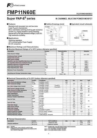
FMP11N60E FUJI POWER MOSFET Super FAP-E3 series N-CHANNEL SILICON POWER MOSFET Features Outline Drawings [mm] Equivalent circuit schematic Maintains both low power loss and low noise TO-220AB Lower R (on) characteristic DS More controllable switching dv/dt by gate resistance Drain(D) Smaller V ringing waveform during switching GS Narrow band of the gate threshold voltage (3.0 0.5V)
0.3. Size:623K fuji
fmp11n70e.pdf 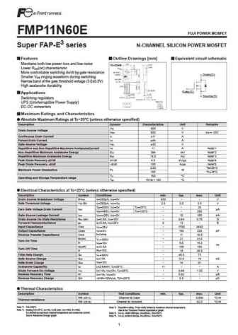
FMP11N60E FUJI POWER MOSFET Super FAP-E3 series N-CHANNEL SILICON POWER MOSFET Features Outline Drawings [mm] Equivalent circuit schematic Maintains both low power loss and low noise TO-220AB Lower R (on) characteristic DS More controllable switching dv/dt by gate resistance Drain(D) Smaller V ringing waveform during switching GS Narrow band of the gate threshold voltage (3.0 0.5V)
0.6. Size:340K trinnotech
tmp11n50sg tmpf11n50sg.pdf 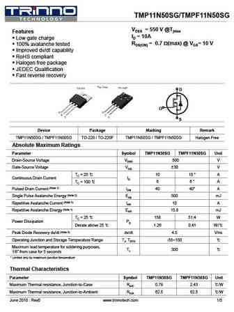
TMP11N50SG/TMPF11N50SG VDSS = 550 V @Tjmax Features ID = 10A Low gate charge RDS(ON) = 0.7 W(max) @ VGS= 10 V 100% avalanche tested Improved dv/dt capability RoHS compliant Halogen free package JEDEC Qualification Fast reverse recovery D G S Device Package Marking Remark TMP11N50SG / TMPF11N50SG TO-220 / TO-220F TMP11N50SG / TMPF11N50SG Halogen Fre
0.7. Size:353K trinnotech
tmp11n50 tmpf11n50.pdf 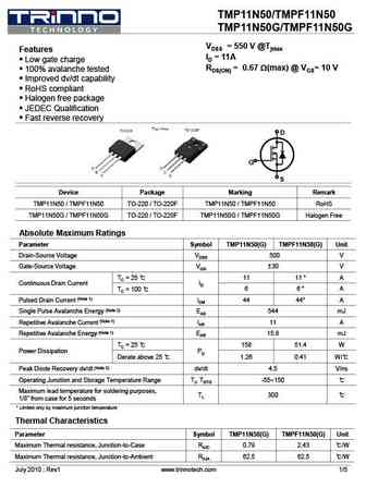
TMP11N50/TMPF11N50 TMP11N50G/TMPF11N50G VDSS = 550 V @Tjmax Features ID = 11A Low gate charge RDS(ON) = 0.67 W(max) @ VGS= 10 V 100% avalanche tested Improved dv/dt capability RoHS compliant Halogen free package JEDEC Qualification Fast reverse recovery D G S Device Package Marking Remark TMP11N50 / TMPF11N50 TO-220 / TO-220F TMP11N50 / TMPF11N50
0.8. Size:790K way-on
wmp119n10lg2.pdf 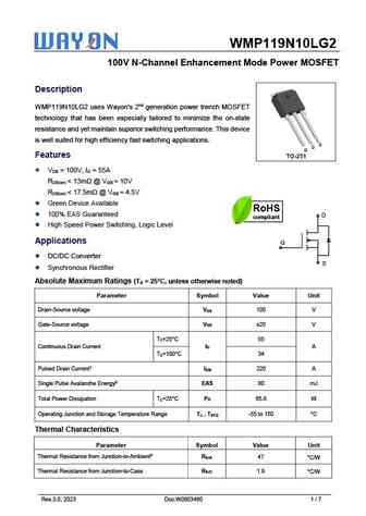
WMP119N10LG2 100V N-Channel Enhancement Mode Power MOSFET Description WMP119N10LG2 uses Wayon's 2nd generation power trench MOSFET technology that has been especially tailored to minimize the on-state resistance and yet maintain superior switching performance. This device is well suited for high efficiency fast switching applications. Features V = 100V, I = 55A DS D R
0.9. Size:674K way-on
wml11n80m3 wmn11n80m3 wmm11n80m3 wmo11n80m3 wmp11n80m3 wmk11n80m3.pdf 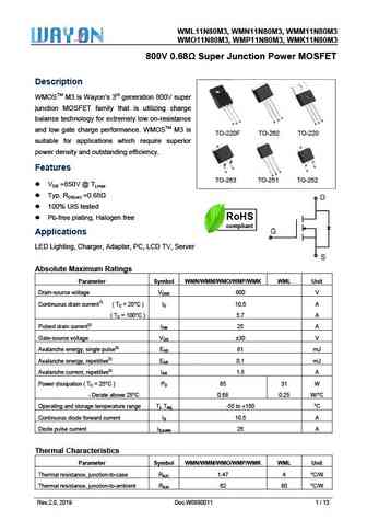
WML11N80M3, W 80M3, WM M3 WMN11N8 MM11N80M WMO1 80M3, WM M3 11N80M3, WMP11N8 MK11N80M 800V 0.68 S T V Super Junction Power MOSFET Descrip ption WMOSTM M3 is Wayo neration 800 M on s 3rd gen 0V super junction MOSFET fa that is utilizing charge M amily S balance te or extremely esistance D echnology fo y low on-re S S G D D G G G T and low ga charge perfo
0.10. Size:664K way-on
wml11n70sr wmk11n70sr wmm11n70sr wmn11n70sr wmp11n70sr wmo11n70sr.pdf 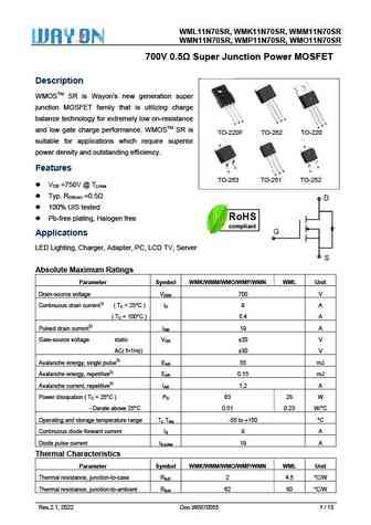
WML11N70SR, W 70SR, WM SR WMK11N7 MM11N70S WMN11N70SR, WMP11N7 MO11N70S 70SR, WM SR 700V 0.5 Su nction P uper Jun Power MOSFET Descrip ption WMOSTM SR is Wa new generation super ayon s w junction MOSFET fa that is utilizing charge M amily S balance te or extremely esistance echnology fo y low on-re D S D G G G S D G T and low ga charge performanc W
0.11. Size:665K way-on
wml11n65sr wmk11n65sr wmm11n65sr wmn11n65sr wmp11n65sr wmo11n65sr.pdf 
WML11N65SR, W 65SR, WM SR WMK11N6 MM11N65S WMN11N65SR, WMP11N6 MO11N65S 65SR, WM SR 650V 0.5 Su nction P uper Jun Power MOSFET Descrip ption WMOSTM SR is Wa new generation super ayon s w junction MOSFET fa that is utilizing charge M amily S balance te or extremely esistance echnology fo y low on-re D S D G G G S D G T and low ga charge performanc W
0.12. Size:540K cn minos
mp11p20.pdf 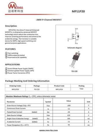
-200V P-Channel MOSFET Description MP11P20, the silicon P-channel Enhanced MOSFETs, is obtained by advanced MOSFET technology which reduce the conduction loss, improve switching performance and enhance the avalanche energy. The transistor is suitable device for SMPS, high speed switching and general purpose applications. Schematic diagram FEATURES Fast switching 100% avalanc
Другие транзисторы: MP101B, MP102, MP103, MP103A, MP104, MP1077, MP10A, MP10B, 2SC945, MP110, MP110B, 2SB1366F-Y, MP110BB, MP110BG, MP110BR, MP110G, MP110O