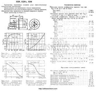
P30. Аналоги и основные параметры
Наименование производителя: P30
Тип материала: Ge
Полярность: PNP
Предельные значения
Максимальная рассеиваемая мощность (Pc): 0.03 W
Макcимально допустимое напряжение коллектор-база (Ucb): 12 V
Макcимальный постоянный ток коллектора (Ic): 0.1 A
Предельная температура PN-перехода (Tj): 75 °C
Электрические характеристики
Граничная частота коэффициента передачи тока (ft): 10 MHz
Ёмкость коллекторного перехода (Cc): 6 pf
Статический коэффициент передачи тока (hFE): 80
Аналоги (замена) для P30
- подборⓘ биполярного транзистора по параметрам
P30 даташит
asdm30p30ctd-r.pdf

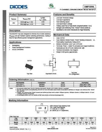
ASDM30P30CTD -30V P-Channel MOSFET Features Product Summary Low RDS(ON) Fast switching V -30 V DSS Green Device Available R 15 m DS(ON)-Typ. Application I -30 A D MB / VGA / Vcore POL Applications DFN3*3-8 P-MOSFET Absolute Maximum Ratings (T =25 C Unless Otherwise Noted) J Symbol Parameter Rating Unit VDSS Drain-Source Voltage -30 V VGSS Gate-
dmp3013sfv-13.pdf
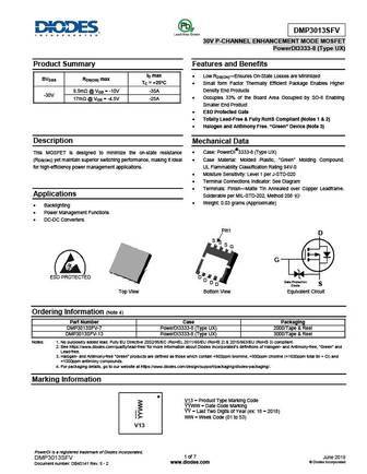
DMP3013SFV 30V P-CHANNEL ENHANCEMENT MODE MOSFET PowerDI3333-8 (Type UX) Product Summary Features and Benefits ID max Low RDS(ON) Ensures On-State Losses are Minimized BVDSS RDS(ON) max TC = +25 C Small form Factor Thermally Efficient Package Enables Higher Density End Products 9.5m @ VGS = -10V -35A -30V Occupies 33% of the Board Area Occupied by SO-8 En
dmp3010lpsq-13.pdf
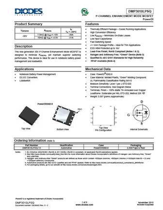
DMP3010LPSQ Green P-CHANNEL ENHANCEMENT MODE MOSFET PowerDI Product Summary Features ID Thermally Efficient Package Cooler Running Applications V(BR)DSS RDS(ON) TA = +25 C High Conversion Efficiency 7.5m @ VGS = -10V -36A Low RDS(ON) Minimizes On-State Losses -30V 10m @ VGS = -4.5V -31A Low Input Capacitance Fast Switching Speed
asdm30p30ctd.pdf
ASDM30P30CTD -30V P-Channel MOSFET Features Product Summary Low RDS(ON) Fast switching V -30 V DSS Green Device Available R 15 m DS(ON)-Typ. Application I -30 A D MB / VGA / Vcore POL Applications DFN3*3-8 P-MOSFET Absolute Maximum Ratings (T =25 C Unless Otherwise Noted) J Symbol Parameter Rating Unit VDSS Drain-Source Voltage -30 V VGSS Gate-
dmp3007sps-13.pdf

DMP3007SPS Green P-CHANNEL ENHANCEMENT MODE MOSFET POWERDI Product Summary Features and Benefits Low RDS(ON) Minimizes On-State Losses ID Max BVDSS RDS(ON) Max Small Form Factor Thermally Efficient Package Enables Higher TC = +25 C Density End Products 7m @ VGS = -10V -90A 100% Unclamped Inductive Switching Ensures More Reliability -30V ESD Pro
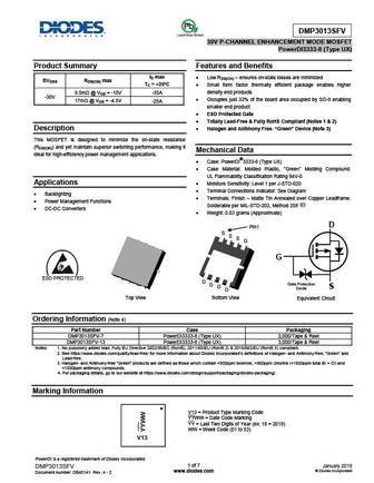
dp3080.pdf
DP3080 TO-252 Datasheet of DP3080 TO-252 18033419374 QQ 2171689052 Shenzhen Developer Microelectronics Co.,Ltd. 707-710 Address Unit 7-10,7/F.,west block, Skyworth Semiconductor design Building, The 4th on High-tech Zone, Nanshan
dmp3013sfv-7.pdf
DMP3013SFV 30V P-CHANNEL ENHANCEMENT MODE MOSFET PowerDI3333-8 (Type UX) Product Summary Features and Benefits ID max Low RDS(ON) ensures on-state losses are minimized BVDSS RDS(ON) max TC = +25 C Small form factor thermally efficient package enables higher density end products 9.5m @ VGS = -10V -35A -30V Occupies just 33% of the board area occupied b
mtp30p06v .pdf

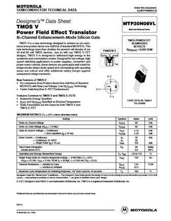
MOTOROLA Order this document SEMICONDUCTOR TECHNICAL DATA by MTP30P06V/D Designer's Data Sheet MTP30P06V TMOS V Motorola Preferred Device Power Field Effect Transistor P Channel Enhancement Mode Silicon Gate TMOS POWER FET TMOS V is a new technology designed to achieve an on resis- 30 AMPERES tance area product about one half that of standard MOSFETs. This 60 VOLTS new
tp3034re.pdf
MOTOROLA Order this document SEMICONDUCTOR TECHNICAL DATA by TP3034/D The RF Line NPN Silicon TP3034 RF Power Transistor The TP3034 is designed for 960 MHz cellular radio base stations in both analog and digital applications. It incoporates high value emitter ballast resistors, gold metallizations and offers a high degree of reliability and ruggedness. Specified 24 Volts, 960 MH
tp3061re.pdf
MOTOROLA Order this document SEMICONDUCTOR TECHNICAL DATA by TP3061/D The RF Line UHF Power Transistor TP3061 The TP3061 is designed for 960 MHz mobile base stations in both analog and digital applications. It incorporates high value emitter ballast resistors, gold metallizations and offers a high degree of reliability and ruggedness. Including double input and output matching network
mtp3055vlrev2a.pdf

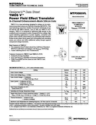
MOTOROLA Order this document SEMICONDUCTOR TECHNICAL DATA by MTP3055VL/D Designer's Data Sheet MTP3055VL TMOS V Motorola Preferred Device Power Field Effect Transistor N Channel Enhancement Mode Silicon Gate TMOS POWER FET TMOS V is a new technology designed to achieve an on resis- 12 AMPERES tance area product about one half that of standard MOSFETs. This 60 VOLTS
mtp30n06vl.pdf
MOTOROLA Order this document SEMICONDUCTOR TECHNICAL DATA by MTP30N06VL/D Designer's Data Sheet MTP30N06VL TMOS V Motorola Preferred Device Power Field Effect Transistor N Channel Enhancement Mode Silicon Gate TMOS POWER FET TMOS V is a new technology designed to achieve an on resis- 30 AMPERES tance area product about one half that of standard MOSFETs. This 60 VOLTS
tp3069re.pdf
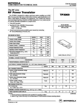
MOTOROLA Order this document SEMICONDUCTOR TECHNICAL DATA by TP3069/D The RF Line RF Power Transistor TP3069 The TP3069 is designed for cellular radio base station amplifiers up to 960 MHz. It incorporates high value emitter ballast resistors, gold metallizations and offers a high degree of reliability and ruggedness. The TP3069 also features input and output matching networks and hig
tp3024br.pdf
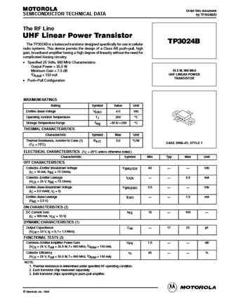
MOTOROLA Order this document SEMICONDUCTOR TECHNICAL DATA by TP3024B/D The RF Line UHF Linear Power Transistor TP3024B The TP3024B is a balanced transistor designed specifically for use in cellular radio systems. This device permits the design of a Class AB push pull, high gain, broadband amplifier having a high degree of linearity without the need for complicated biasing circuitry.
tp3005re.pdf

MOTOROLA Order this document SEMICONDUCTOR TECHNICAL DATA by TP3005/D The RF Line UHF Power Transistor TP3005 The TP3005 is designed for 960 MHz base stations in both analog and digital applications. It incorporates high value emitter ballast resistors, gold metalliza- tions and offers a high degree of reliability and ruggedness. Specified 26 Volts, 960 MHz Characteristics Output
tp3021re.pdf
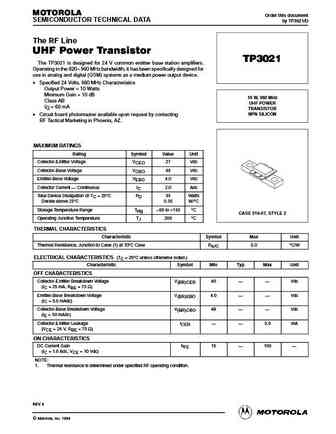
MOTOROLA Order this document SEMICONDUCTOR TECHNICAL DATA by TP3021/D The RF Line UHF Power Transistor TP3021 The TP3021 is designed for 24 V common emitter base station amplifiers. Operating in the 820 960 MHz bandwidth, it has been specifically designed for use in analog and digital (GSM) systems as a medium power output device. Specified 24 Volts, 960 MHz Characteristics Out
mtp3055vl.pdf
MOTOROLA Order this document SEMICONDUCTOR TECHNICAL DATA by MTP3055VL/D Designer's Data Sheet MTP3055VL TMOS V Motorola Preferred Device Power Field Effect Transistor N Channel Enhancement Mode Silicon Gate TMOS POWER FET TMOS V is a new technology designed to achieve an on resis- 12 AMPERES tance area product about one half that of standard MOSFETs. This 60 VOLTS
tp3006re.pdf
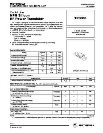
MOTOROLA Order this document SEMICONDUCTOR TECHNICAL DATA by TP3006/D The RF Line NPN Silicon TP3006 RF Power Transistor The TP3006 is designed for cellular radio base station amplifiers up to 960 MHz. It incorporates high value emitter ballast resistors, gold metallizations and offers a high degree of reliability and ruggedness. The TP3006 also features input and output matching net
tp3008re.pdf
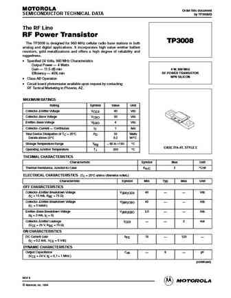
MOTOROLA Order this document SEMICONDUCTOR TECHNICAL DATA by TP3008/D The RF Line RF Power Transistor TP3008 The TP3008 is designed for 960 MHz cellular radio base stations in both analog and digital applications. It incorporates high value emitter ballast resistors, gold metallizations and offers a high degree of reliability and ruggedness. Specified 24 Volts, 960 MHz Characteri
tp3022br.pdf
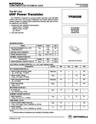
MOTOROLA Order this document SEMICONDUCTOR TECHNICAL DATA by TP3022B/D The RF Line UHF Power Transistor TP3022B The TP3022B is designed for common emitter operation in the 900 MHz mobile radio band. Use of gold metallization and silicon diffused ballast resistors results in a medium power output/driver transistor with state of the art ruggedness and reliability. Specifie
tp3007sr.pdf
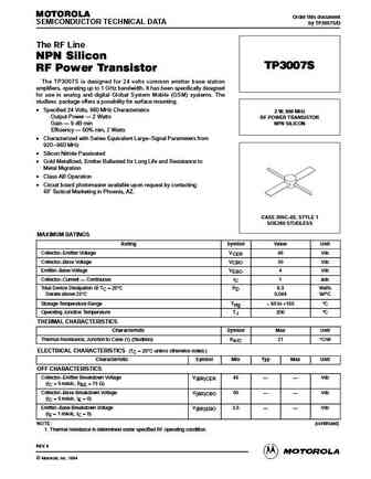
MOTOROLA Order this document SEMICONDUCTOR TECHNICAL DATA by TP3007S/D The RF Line NPN Silicon TP3007S RF Power Transistor The TP3007S is designed for 24 volts common emitter base station amplifiers, operating up to 1 GHz bandwidth. It has been specifically designed for use in analog and digital Global System Mobile (GSM) systems. The studless package offers a possibility for surface
mtp3055vrev2a.pdf

MOTOROLA Order this document SEMICONDUCTOR TECHNICAL DATA by MTP3055V/D Designer's Data Sheet MTP3055V TMOS V Motorola Preferred Device Power Field Effect Transistor N Channel Enhancement Mode Silicon Gate TMOS POWER FET TMOS V is a new technology designed to achieve an on resis- 12 AMPERES tance area product about one half that of standard MOSFETs. This 60 VOLTS
mtp3055v.pdf
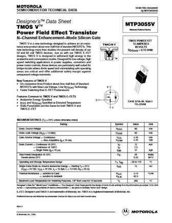
MOTOROLA Order this document SEMICONDUCTOR TECHNICAL DATA by MTP3055V/D Designer's Data Sheet MTP3055V TMOS V Motorola Preferred Device Power Field Effect Transistor N Channel Enhancement Mode Silicon Gate TMOS POWER FET TMOS V is a new technology designed to achieve an on resis- 12 AMPERES tance area product about one half that of standard MOSFETs. This 60 VOLTS
tp3032re.pdf
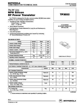
MOTOROLA Order this document SEMICONDUCTOR TECHNICAL DATA by TP3032/D The RF Line NPN Silicon TP3032 RF Power Transistor The TP3032 is designed for 26 volts, common emitter, 960 MHz base station amplifiers, for use in analog and digital systems. Specified 26 Volts, 960 MHz Characteristics Output Power 21 Watts Gain 7.5 dB min 21 W, 960 MHz RF POWER TRANSISTOR Sili
mtp30p06v.pdf
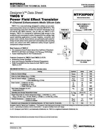
MOTOROLA Order this document SEMICONDUCTOR TECHNICAL DATA by MTP30P06V/D Designer's Data Sheet MTP30P06V TMOS V Motorola Preferred Device Power Field Effect Transistor P Channel Enhancement Mode Silicon Gate TMOS POWER FET TMOS V is a new technology designed to achieve an on resis- 30 AMPERES tance area product about one half that of standard MOSFETs. This 60 VOLTS new
irfp3077pbf.pdf
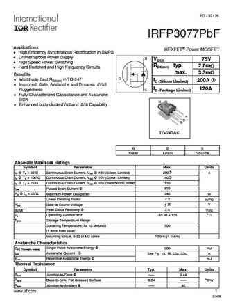
PD - 97126 IRFP3077PbF Applications HEXFET Power MOSFET l High Efficiency Synchronous Rectification in SMPS l Uninterruptible Power Supply D VDSS 75V l High Speed Power Switching RDS(on) typ. 2.8m l Hard Switched and High Frequency Circuits max. 3.3m Benefits G l Worldwide Best RDS(on) in TO-247 ID (Silicon Limited) 200A c l Improved Gate, Avalanche and Dynamic dV/d
irfp3006.pdf
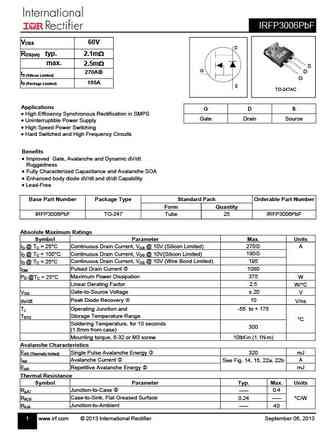
IRFP3006PbF VDSS 60V D RDS(on) typ. 2.1m max. 2.5m S G D 270A ID (Silicon Limited) G ID (Package Limited) 195A S TO-247AC Applications G D S High Efficiency Synchronous Rectification in SMPS Gate Drain Source Uninterruptible Power Supply High Speed Power Switching Hard Switched and High Frequency Circuits Benefits Improved
irgp30b60kd-e.pdf
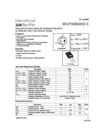
PD - 94388B IRGP30B60KD-E INSULATED GATE BIPOLAR TRANSISTOR WITH ULTRAFAST SOFT RECOVERY DIODE Features C VCES = 600V Low VCE (on) Non Punch Through IGBT Technology. Low Diode VF. 10 s Short Circuit Capability. IC = 30A, TC=100 C Square RBSOA. Ultrasoft Diode Reverse Recovery Characteristics. G tsc > 10 s, TJ=150 C Positive VCE (on) Temperature Coeffici
irgp30b120kd-e.pdf
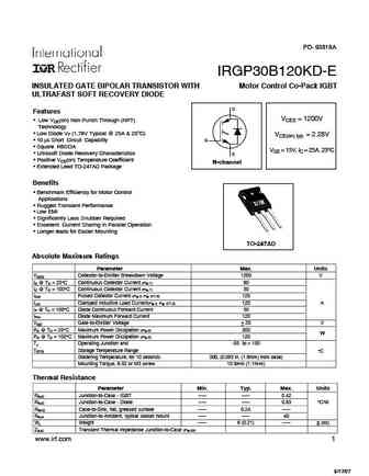
PD- 93818A IRGP30B120KD-E INSULATED GATE BIPOLAR TRANSISTOR WITH Motor Control Co-Pack IGBT ULTRAFAST SOFT RECOVERY DIODE C Features VCES = 1200V Low VCE(on) Non Punch Through (NPT) Technology Low Diode VF (1.76V Typical @ 25A & 25 C) VCE(on) typ. = 2.28V 10 s Short Circuit Capability G Square RBSOA VGE = 15V, IC = 25A, 25 C Ultrasoft Diode Recovery Ch
irlp3034pbf.pdf
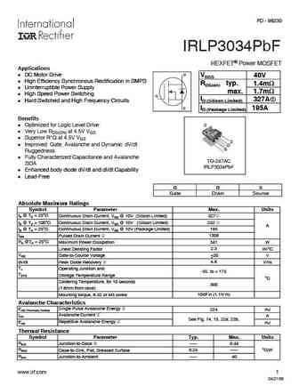
PD - 96230 IRLP3034PbF HEXFET Power MOSFET Applications D l DC Motor Drive VDSS 40V l High Efficiency Synchronous Rectification in SMPS RDS(on) typ. 1.4m l Uninterruptible Power Supply max. 1.7m l High Speed Power Switching G ID (Silicon Limited) 327A l Hard Switched and High Frequency Circuits S ID (Package Limited) 195A Benefits l Optimized for Logic Level Drive D
php30nq15t phb30nq15t.pdf
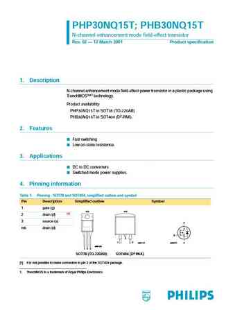
PHP30NQ15T; PHB30NQ15T N-channel enhancement mode field-effect transistor Rev. 02 12 March 2001 Product specification 1. Description N-channel enhancement mode field-effect power transistor in a plastic package using TrenchMOS 1 technology. Product availability PHP30NQ15T in SOT78 (TO-220AB) PHB30NQ15T in SOT404 (D2-PAK). 2. Features Fast switching Low on-state resistance.
phd3055e php3055e 4.pdf
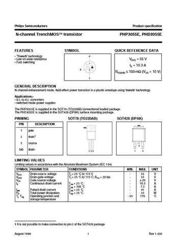
Philips Semiconductors Product specification N-channel TrenchMOS transistor PHP3055E, PHD3055E FEATURES SYMBOL QUICK REFERENCE DATA Trench technology d Low on-state resistance VDSS = 55 V Fast switching ID = 10.3 A g RDS(ON) 150 m (VGS = 10 V) s GENERAL DESCRIPTION N-channel enhancement mode, field-effect power transistor in a plastic envelope using tr
php3055e phd3055e.pdf
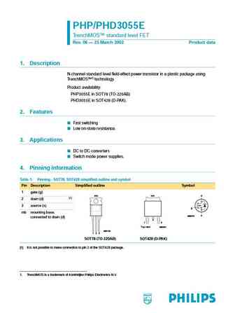
PHP/PHD3055E TrenchMOS standard level FET Rev. 06 25 March 2002 Product data 1. Description N-channel standard level field-effect power transistor in a plastic package using TrenchMOS 1 technology. Product availability PHP3055E in SOT78 (TO-220AB) PHD3055E in SOT428 (D-PAK). 2. Features Fast switching Low on-state resistance. 3. Applications DC to DC converters Switc
php3055l 2.pdf
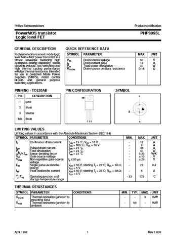
Philips Semiconductors Product specification PowerMOS transistor PHP3055L Logic level FET GENERAL DESCRIPTION QUICK REFERENCE DATA N-channel enhancement mode logic SYMBOL PARAMETER MAX. UNIT level field-effect power transistor in a plastic envelope featuring high VDS Drain-source voltage 60 V avalanche energy capability, stable ID Drain current (DC) 12 A blocking voltage, fast switch
phb30nq15t php30nq15t 1.pdf
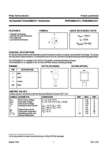
Philips Semiconductors Product specification N-channel TrenchMOS transistor PHP30NQ15T, PHB30NQ15T FEATURES SYMBOL QUICK REFERENCE DATA Trench technology d Very low on-state resistance VDSS = 150 V Fast switching Low thermal resistance ID = 29 A g RDS(ON) 63 m s GENERAL DESCRIPTION N-channel enhancement mode field-effect power transistor in a plastic
bsp304a.pdf

DISCRETE SEMICONDUCTORS DATA SHEET BSP304; BSP304A P-channel enhancement mode vertical D-MOS transistors 1995 Apr 07 Product specification File under Discrete Semiconductors, SC07 Philips Semiconductors Philips Semiconductors Product specification P-channel enhancement mode BSP304; BSP304A vertical D-MOS transistors FEATURES DESCRIPTION Direct interface to C-MOS, TTL etc. P-c
bsp304.pdf
DISCRETE SEMICONDUCTORS DATA SHEET BSP304; BSP304A P-channel enhancement mode vertical D-MOS transistors 1995 Apr 07 Product specification File under Discrete Semiconductors, SC07 Philips Semiconductors Philips Semiconductors Product specification P-channel enhancement mode BSP304; BSP304A vertical D-MOS transistors FEATURES DESCRIPTION Direct interface to C-MOS, TTL etc. P-c
php3055e 1.pdf
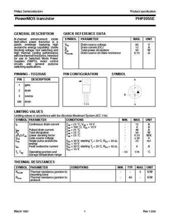
Philips Semiconductors Product specification PowerMOS transistor PHP3055E GENERAL DESCRIPTION QUICK REFERENCE DATA N-channel enhancement mode SYMBOL PARAMETER MAX. UNIT field-effect power transistor in a plastic envelope featuring high VDS Drain-source voltage 60 V avalanche energy capability, stable ID Drain current (DC) 12 A blocking voltage, fast switching and Ptot Total power dissi
phb3055e phd3055e php3055e 3.pdf
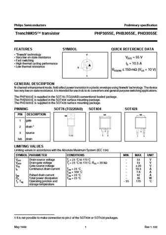
Philips Semiconductors Preliminary specification TrenchMOS transistor PHP3055E, PHB3055E, PHD3055E FEATURES SYMBOL QUICK REFERENCE DATA Trench technology d Very low on-state resistance VDSS = 55 V Fast switching High thermal cycling performance ID = 10.5 A Low thermal resistance g RDS(ON) 150 m (VGS = 10 V) s GENERAL DESCRIPTION N-channel enhance
stp30ne06.pdf

STP30NE06 STP30NE06FP N - CHANNEL 60V - 0.042 - 30A - TO-220/TO-220FP STripFET POWER MOSFET PRELIMINARY DATA TYPE VDSS RDS(on) ID STP30NE06 60 V
stp3020l.pdf
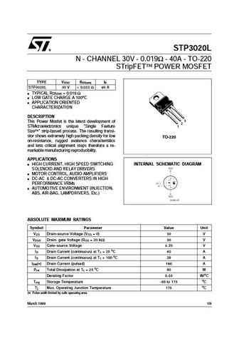
STP3020L N - CHANNEL 30V - 0.019 - 40A - TO-220 STripFET POWER MOSFET TYPE VDSS RDS(on) ID STP3020L 30 V
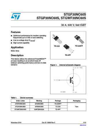
stgf30nc60s stgp30nc60s stgwf30nc60s.pdf
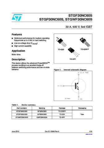
STGF30NC60S STGP30NC60S, STGWF30NC60S 30 A, 600 V, fast IGBT Features TAB Optimized performance for medium operating frequencies up to 5 kHz in hard switching Low on-voltage drop (VCE(sat)) 3 3 2 High current capability 2 1 1 TO-220 TO-220FP Application 1 1 1 3 Motor drive 2 1 TO-3PF Description This device utilizes the advanced PowerMESHTM process result
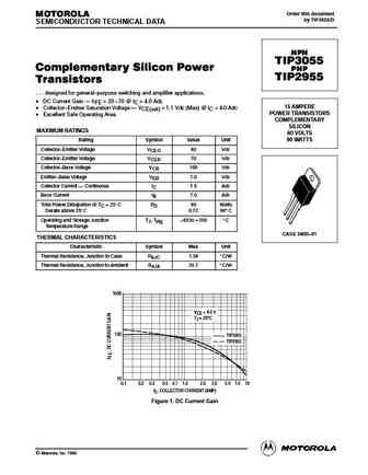
tip2955 tip3055.pdf
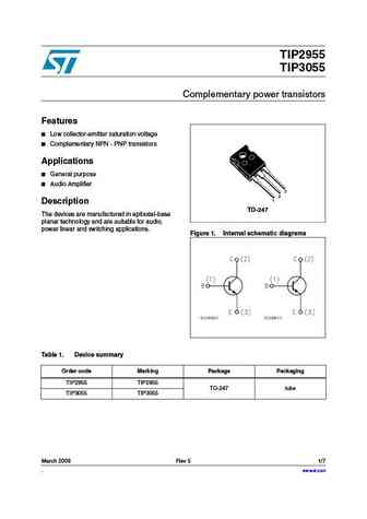
TIP2955 TIP3055 Complementary power transistors Features Low collector-emitter saturation voltage Complementary NPN - PNP transistors Applications General purpose Audio Amplifier 3 2 1 Description TO-247 The devices are manufactured in epitaxial-base planar technology and are suitable for audio, power linear and switching applications. Figure 1. Internal sche
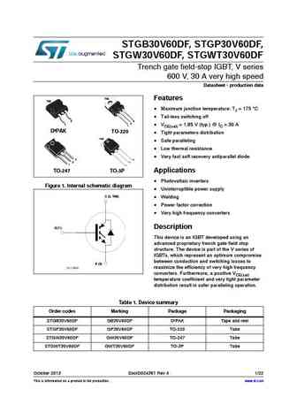
stgb30v60df stgp30v60df stgw30v60df stgwt30v60df.pdf

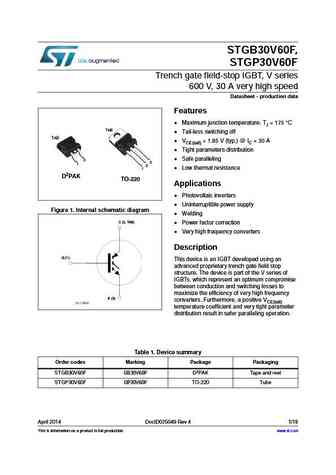
STGB30V60DF, STGP30V60DF, STGW30V60DF, STGWT30V60DF Trench gate field-stop IGBT, V series 600 V, 30 A very high speed Datasheet - production data TAB Features TAB Maximum junction temperature TJ = 175 C Tail-less switching off 3 3 2 1 VCE(sat) = 1.85 V (typ.) @ IC = 30 A 1 D PAK TO-220 Tight parameters distribution TAB Safe paralleling Low therma
stp30ns15lfp.pdf
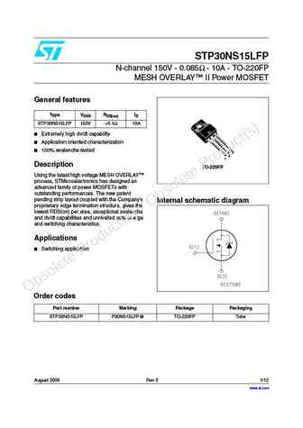
STP30NS15LFP N-channel 150V - 0.085 - 10A - TO-220FP MESH OVERLAY II Power MOSFET General features Type VDSS RDS(on) ID STP30NS15LFP 150V
stgb30nc60k stgp30nc60k.pdf
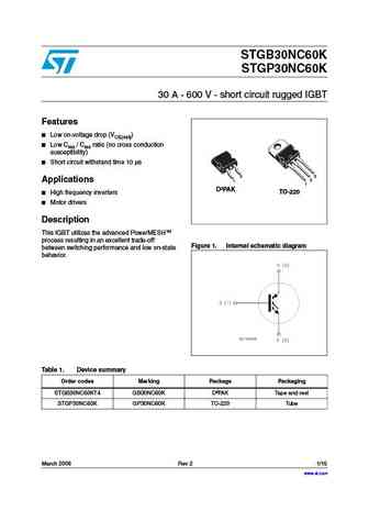
STGB30NC60K STGP30NC60K 30 A - 600 V - short circuit rugged IGBT Features Low on-voltage drop (VCE(sat)) Low Cres / Cies ratio (no cross conduction susceptibility) Short circuit withstand time 10 s 3 3 2 Applications 1 1 D PAK TO-220 High frequency inverters Motor drivers Description This IGBT utilizes the advanced PowerMESH process resulting in an
stp30nm30n.pdf
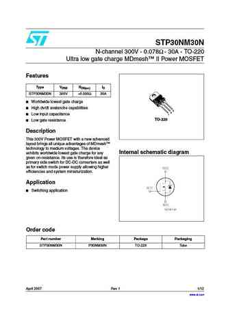
STP30NM30N N-channel 300V - 0.078 - 30A - TO-220 Ultra low gate charge MDmesh II Power MOSFET Features Type VDSS RDS(on) ID STP30NM30N 300V
tip29a-tip29c tip30a-tip30c.pdf
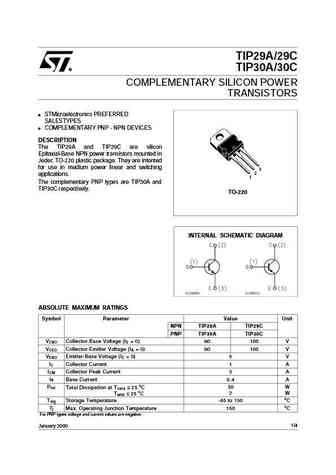
TIP29A/29C TIP30A/30C COMPLEMENTARY SILICON POWER TRANSISTORS STMicroelectronics PREFERRED SALESTYPES COMPLEMENTARY PNP - NPN DEVICES DESCRIPTION The TIP29A and TIP29C are silicon Epitaxial-Base NPN power transistors mounted in Jedec TO-220 plastic package. They are intented for use in medium power linear and switching 3 2 applications. 1 The complementary PNP types ar
stgp30h60df.pdf
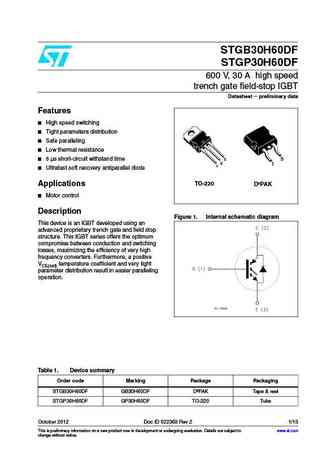
STGB30H60DF STGP30H60DF 600 V, 30 A high speed trench gate field-stop IGBT Datasheet - preliminary data Features High speed switching Tight parameters distribution Safe paralleling Low thermal resistance 6 s short-circuit withstand time 3 3 2 1 1 Ultrafast soft recovery antiparallel diode TO-220 Applications D PAK Motor control Description Fig
stp30ne06l.pdf
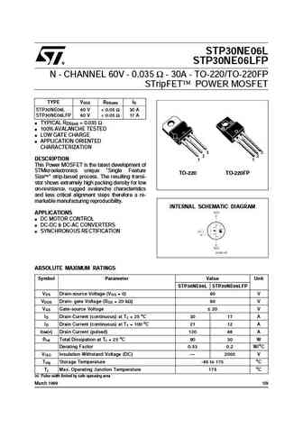
STP30NE06L STP30NE06LFP N - CHANNEL 60V - 0.035 - 30A - TO-220/TO-220FP STripFET POWER MOSFET TYPE VDSS RDS(on) ID STP30NE06L 60 V
stb30nf10 stp30nf10 stp30nf10fp.pdf
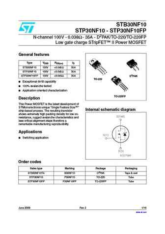
STB30NF10 STP30NF10 - STP30NF10FP N-channel 100V - 0.038 - 35A - D2PAK/TO-220/TO-220FP Low gate charge STripFET II Power MOSFET General features Type VDSS RDS(on) ID STB30NF10 100V
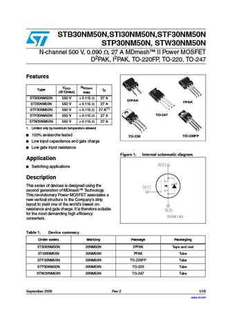
stb30nm60n stf30nm60n stp30nm60n stw30nm60n.pdf
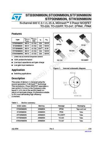
STB30NM60N,STI30NM60N,STF30NM60N STP30NM60N, STW30NM60N N-channel 600 V, 0.1 , 25 A, MDmesh II Power MOSFET TO-220, TO-220FP, TO-247, D2PAK, I2PAK Features RDS(on) VDSS @ Type ID PW TJmax max 3 3 1 2 1 STB30NM60N 650 V
stb300nh02l stp300nh02l.pdf

STB300NH02L STP300NH02L N-channel 24V - 120A - TO-220 / D2PAK STripFET Power MOSFET Preliminary Data Features Type VDSS RDS(on) Max ID STB300NH02L 24V
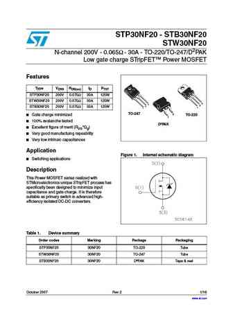
stp30nf20 stw30nf20.pdf
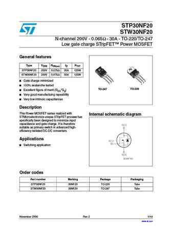
STP30NF20 STW30NF20 N-channel 200V - 0.065 - 30A - TO-220/TO-247 Low gate charge STripFET Power MOSFET General features Type VDSS RDS(on) ID PTOT STP30NF20 200V 0.075 30A 125W STW30NF20 200V 0.075 30A 125W Gate charge minimized 3 3 2 2 1 1 100% avalanche tested TO-220 TO-247 Excellent figure of merit (RDS*Qg) Very good manufactuing repeability Ver
stp30n05.pdf
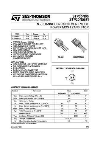
STP30N05 STP30N05FI N - CHANNEL ENHANCEMENT MODE POWER MOS TRANSISTOR TYPE VDSS RDS(on) ID STP30N05 50 V
stp30ne06l-fp.pdf

STP30NE06L STP30NE06LFP N - CHANNEL 60V - 0.035 - 30A - TO-220/TO-220FP STripFET POWER MOSFET TYPE VDSS RDS(on) ID STP30NE06L 60 V
stp30nf20 stb30nf20 stw30nf20.pdf

STP30NF20 - STB30NF20 STW30NF20 N-channel 200V - 0.065 - 30A - TO-220/TO-247/D2PAK Low gate charge STripFET Power MOSFET Features Type VDSS RDS(on) ID PTOT STP30NF20 200V 0.075 30A 125W STW30NF20 200V 0.075 30A 125W 3 3 2 2 STB30NF20 200V 0.075 30A 125W 1 1 TO-247 3 Gate charge minimized TO-220 1 100% avalanche tested D PAK Excellent figure of me
stb30nf10t4 stb30nf10 stp30nf10 stp30nf10fp.pdf

STB30NF10 STP30NF10 - STP30NF10FP N-channel 100V - 0.038 - 35A - D2PAK/TO-220/TO-220FP Low gate charge STripFET II Power MOSFET General features Type VDSS RDS(on) ID STB30NF10 100V
bsp30 bsp31 bsp32 bsp33.pdf
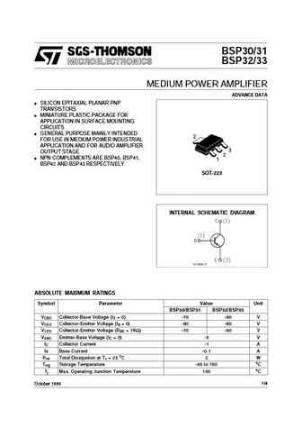
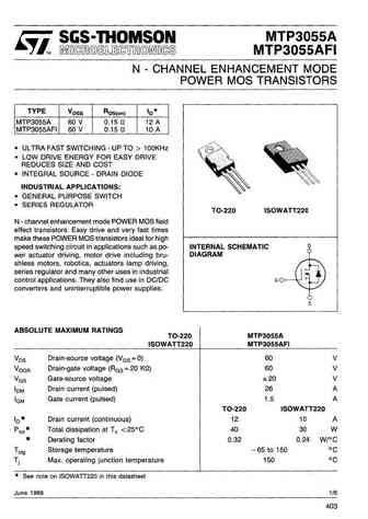
BSP30/31 BSP32/33 MEDIUM POWER AMPLIFIER ADVANCE DATA SILICON EPITAXIAL PLANAR PNP TRANSISTORS MINIATURE PLASTIC PACKAGE FOR APPLICATION IN SURFACE MOUNTING CIRCUITS GENERAL PURPOSE MAINLY INTENDED 2 FOR USE IN MEDIUM POWER INDUSTRIAL APPLICATION AND FOR AUDIO AMPLIFIER 3 OUTPUT STAGE 2 NPN COMPLEMENTS ARE BSP40, BSP41, 1 BSP42 AND BSP43 RESPECTIVELY SOT-223 INTERNAL SCH
stgp30nc60s.pdf
STGF30NC60S STGP30NC60S, STGWF30NC60S 30 A, 600 V, fast IGBT Features TAB Optimized performance for medium operating frequencies up to 5 kHz in hard switching Low on-voltage drop (VCE(sat)) 3 3 2 High current capability 2 1 1 TO-220 TO-220FP Application 1 1 1 3 Motor drive 2 1 TO-3PF Description This device utilizes the advanced PowerMESH process resul
stp30n06.pdf

STP30N06 STP30N06FI N - CHANNEL ENHANCEMENT MODE POWER MOS TRANSISTOR TYPE VDSS RDS(on) ID STP30N06 60 V
stb30nm50n sti30nm50n stf30nm50n stp30nm50n stw30nm50n.pdf
STB30NM50N,STI30NM50N,STF30NM50N STP30NM50N, STW30NM50N N-channel 500 V, 0.090 , 27 A MDmesh II Power MOSFET D2PAK, I2PAK, TO-220FP, TO-220, TO-247 Features RDS(on) VDSS Type ID (@Tjmax) max 3 3 1 2 1 STB30NM50N 550 V
stgp30m65df2.pdf
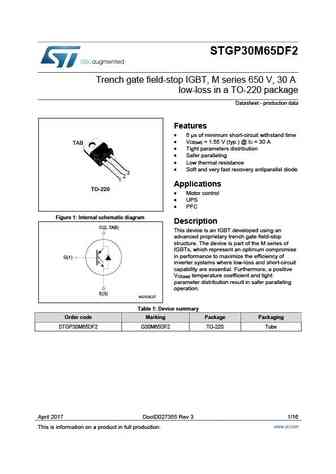
STGP30M65DF2 Trench gate field-stop IGBT, M series 650 V, 30 A low-loss in a TO-220 package Datasheet - production data Features 6 s of minimum short-circuit withstand time V = 1.55 V (typ.) @ I = 30 A CE(sat) C TAB Tight parameters distribution Safer paralleling Low thermal resistance Soft and very fast recovery antiparallel diode 3 2 1 Appl
stgb30h60df stgf30h60df stgp30h60df stgw30h60df.pdf
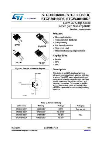
STGB30H60DF, STGF30H60DF, STGP30H60DF, STGW30H60DF 600 V, 30 A high speed trench gate field-stop IGBT Datasheet - production data Features TAB High speed switching Tight parameters distribution 3 1 3 Safe paralleling 2 1 D PAK Low thermal resistance TO-220FP Short circuit rated TAB Ultrafast soft recovery antiparallel diode Applications 3 3 I
stgp30v60df.pdf
STGB30V60DF, STGP30V60DF, STGW30V60DF, STGWT30V60DF Trench gate field-stop IGBT, V series 600 V, 30 A very high speed Datasheet - production data TAB Features TAB Maximum junction temperature TJ = 175 C Tail-less switching off 3 3 2 1 VCE(sat) = 1.85 V (typ.) @ IC = 30 A 1 D PAK TO-220 Tight parameters distribution TAB Safe paralleling Low therma
stb30n65m5 stf30n65m5 sti30n65m5 stp30n65m5 stw30n65m5.pdf
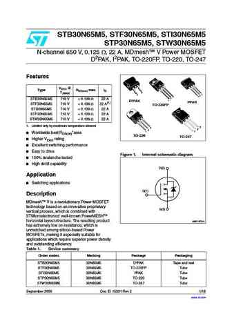
STB30N65M5, STF30N65M5, STI30N65M5 STP30N65M5, STW30N65M5 N-channel 650 V, 0.125 , 22 A, MDmesh V Power MOSFET D2PAK, I2PAK, TO-220FP, TO-220, TO-247 Features VDSS @ Type RDS(on) max ID TJMAX 3 3 1 2 3 1 2 STB30N65M5 710 V
stp300nh02l.pdf
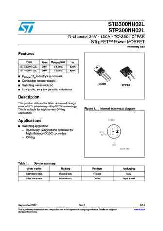
STB300NH02L STP300NH02L N-channel 24V - 120A - TO-220 / D2PAK STripFET Power MOSFET Preliminary Data Features Type VDSS RDS(on) Max ID STB300NH02L 24V
stgb30h60dfb stgp30h60dfb.pdf
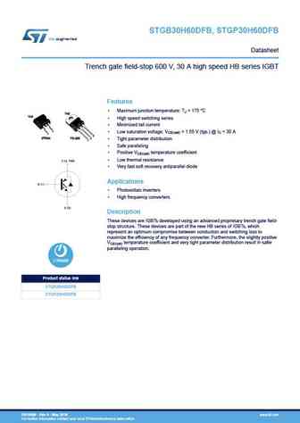
STGB30H60DFB, STGP30H60DFB Datasheet Trench gate field-stop 600 V, 30 A high speed HB series IGBT Features Maximum junction temperature TJ = 175 C TAB TAB High speed switching series Minimized tail current 3 Low saturation voltage VCE(sat) = 1.55 V (typ.) @ IC = 30 A 1 3 2 D PAK TO-220 2 Tight parameter distribution 1 Safe paralleling Positive V
stp30ne06-fp.pdf
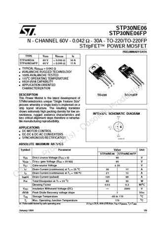
STP30NE06 STP30NE06FP N - CHANNEL 60V - 0.042 - 30A - TO-220/TO-220FP STripFET POWER MOSFET PRELIMINARY DATA TYPE VDSS RDS(on) ID STP30NE06 60 V
stb30nm60n sti30nm60n stf30nm60n stp30nm60n stw30nm60n.pdf

STB30NM60N,STI30NM60N,STF30NM60N STP30NM60N, STW30NM60N N-channel 600 V, 0.1 , 25 A, MDmesh II Power MOSFET TO-220, TO-220FP, TO-247, D2PAK, I2PAK Features RDS(on) VDSS @ Type ID PW TJmax max 3 3 1 2 1 STB30NM60N 650 V
stw30nm60nd stp30nm60nd stf30nm60nd sti30nm60nd stb30nm60nd.pdf
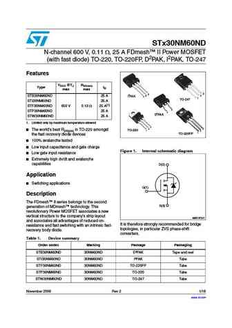
STx30NM60ND N-channel 600 V, 0.11 , 25 A FDmesh II Power MOSFET (with fast diode) TO-220, TO-220FP, D2PAK, I2PAK, TO-247 Features VDSS @TJ RDS(on) Type ID max max 3 3 2 2 2 STB30NM60ND 25 A I PAK 1 1 TO-247 STI30NM60ND 25 A STF30NM60ND 650 V 0.13 25 A(1) 3 STP30NM60ND 25 A 1 2 D PAK STW30NM60ND 25 A 1. Limited only by maximum temperature allowed 3 2 3 T
stf30nm60nd stp30nm60nd stw30nm60nd.pdf

STx30NM60ND N-channel 600 V, 0.11 , 25 A FDmesh II Power MOSFET (with fast diode) TO-220, TO-220FP, D2PAK, I2PAK, TO-247 Features VDSS @TJ RDS(on) Type ID max max 3 3 2 2 2 STB30NM60ND 25 A I PAK 1 1 TO-247 STI30NM60ND 25 A STF30NM60ND 650 V 0.13 25 A(1) 3 STP30NM60ND 25 A 1 2 D PAK STW30NM60ND 25 A 1. Limited only by maximum temperature allowed 3 2 3 T
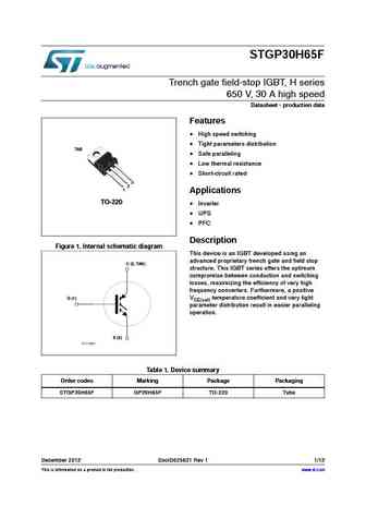
stgp30h65f.pdf
STGP30H65F Trench gate field-stop IGBT, H series 650 V, 30 A high speed Datasheet - production data Features High speed switching Tight parameters distribution TAB Safe paralleling Low thermal resistance Short-circuit rated 3 2 1 Applications TO-220 Inverter UPS PFC Description Figure 1. Internal schematic diagram This device is an IGBT deve
stp30nf20 stw30nf20 stb30nf20.pdf
STP30NF20 - STB30NF20 STW30NF20 N-channel 200V - 0.065 - 30A - TO-220/TO-247/D2PAK Low gate charge STripFET Power MOSFET Features Type VDSS RDS(on) ID PTOT STP30NF20 200V 0.075 30A 125W STW30NF20 200V 0.075 30A 125W 3 3 2 2 STB30NF20 200V 0.075 30A 125W 1 1 TO-247 3 Gate charge minimized TO-220 1 100% avalanche tested D PAK Excellent figure of me
stgp30v60f.pdf
STGB30V60F, STGP30V60F Trench gate field-stop IGBT, V series 600 V, 30 A very high speed Datasheet - production data Features Maximum junction temperature TJ = 175 C TAB Tail-less switching off TAB VCE(sat) = 1.85 V (typ.) @ IC = 30 A Tight parameters distribution Safe paralleling 3 3 1 2 1 Low thermal resistance D2PAK TO-220 Applications Ph
mtp3055e.pdf
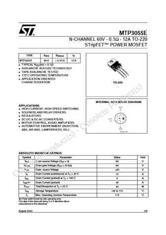
MTP3055E N-CHANNEL 60V - 0.1 - 12ATO-220 STripFET POWER MOSFET TYPE VDSS RDS(on) ID MTP3055E 60 V
fp302.pdf
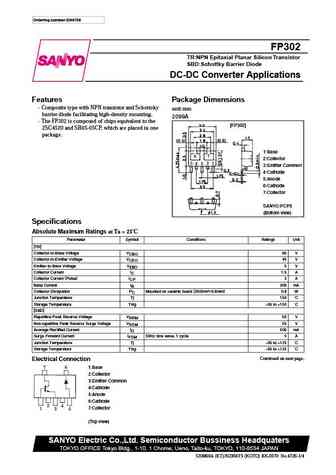
Ordering number EN4726 FP302 TR NPN Epitaxial Planar Silicon Transistor SBD Schottky Barrier Diode DC-DC Converter Applications Features Package Dimensions Composite type with NPN transistor and Schottoky unit mm barrier diode facilitating high-density mounting. 2099A The FP302 is composed of chips equivalent to the [FP302] 2SC4520 and SB05-05CP, which are placed in one pac
fp301.pdf
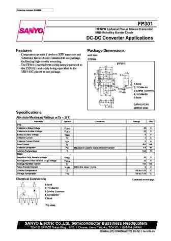
Ordering number EN4539 FP301 TR NPN Epitaxial Planar Silicon Transistor SBD Schottky Barrier Diode DC-DC Converter Applications Features Package Dimensions Composite type with 2 devices (NPN transistor and unit mm Schottoky barrier diode) contained in one package, 2099A facilitating high-density mounting. [FP301] The FP301 is formed with a chip being equivalent to the 2SD16
atp301.pdf
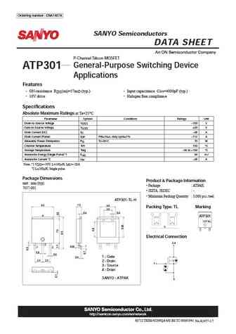
ATP301 Ordering number ENA1457A SANYO Semiconductors DATA SHEET P-Channel Silicon MOSFET General-Purpose Switching Device ATP301 Applications Features ON-resistance RDS(on)=57m (typ.) Input capacitance Ciss=4000pF (typ.) 10V drive Halogen free compliance Specifications at Ta=25 C Absolute Maximum Ratings Parameter Symbol Conditions Ratings Unit Drain-
fp304.pdf
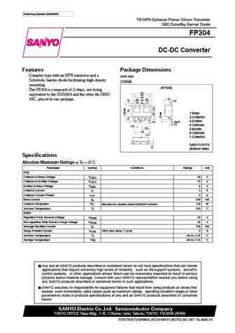
Ordering number ENN4926 TR NPN Epitaxial Planar Silicon Transistor SBD Schottky Barrier Diode FP304 DC-DC Converter Features Package Dimensions Complex type with an NPN transistor and a unit mm Schottoky barrier diode facilitating high-density 2099A mounting. [FP304] The FP304 is composed of 2 chips, one being 4.5 equivalent to the 2SD1620 and the other the SB07- 3.4 2.8
smp3003-dl-e.pdf
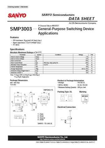
SMP3003 Ordering number ENA1655B SANYO Semiconductors DATA SHEET P-Channel Silicon MOSFET General-Purpose Switching Device SMP3003 Applications Features ON-resistance RDS(on)1=6.2m (typ.) Input capacitance Ciss=13400pF (typ.) 4V drive Specifications at Ta=25 C Absolute Maximum Ratings Parameter Symbol Conditions Ratings Unit Drain-to-Source Voltage VDSS --75
atp302.pdf
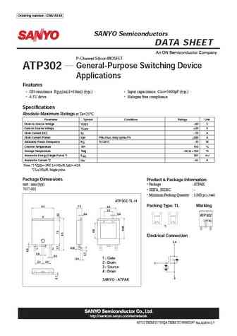
ATP302 Ordering number ENA1654A SANYO Semiconductors DATA SHEET P-Channel Silicon MOSFET General-Purpose Switching Device ATP302 Applications Features ON-resistance RDS(on)1=10m (typ.) Input capacitance Ciss=5400pF (typ.) 4.5V drive Halogen free compliance Specifications at Ta=25 C Absolute Maximum Ratings Parameter Symbol Conditions Ratings Unit Drai
fp303.pdf
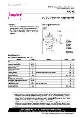
Ordering number ENN4657 TR NPN Epitaxial Planar Silicon Transistor SBD Schottky Barrier Diode FP303 DC-DC Converter Applications Features Package Dimensions Composite type with NPN transistor and Schottoky unit mm barrier diode facilitates high-density mounting. 2099A The FP303 is composed of chips equivalent to the [FP303] 2SD1623 and SB05-05CP, which are placed in one 4.5
smp3003.pdf

SMP3003 Ordering number ENA1655A SANYO Semiconductors DATA SHEET P-Channel Silicon MOSFET General-Purpose Switching Device SMP3003 Applications Features ON-resistance RDS(on)1=6.2m (typ.) Input capacitance Ciss=13400pF 4V drive Specifications at Ta=25 C Absolute Maximum Ratings Parameter Symbol Conditions Ratings Unit Drain-to-Source Voltage VDSS --75 V Gat
rjp30k3dpp-m0.pdf
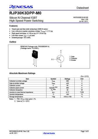
Preliminary Datasheet RJP30K3DPP-M0 R07DS0501EJ0100 Silicon N Channel IGBT Rev.1.00 High Speed Power Switching Jul 05, 2011 Features Trench gate and thin wafer technology (G6H-II series) Low collector to emitter saturation voltage VCE(sat) = 1.1V typ High speed switching tr = 90 ns typ, tf = 250 ns typ Low leak current ICES = 1 A max Isolated package
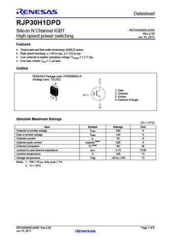
rjp30h1dpd.pdf

Preliminary Datasheet RJP30H1DPD R07DS0465EJ0200 Silicon N Channel IGBT Rev.2.00 High speed power switching Jun 15, 2011 Features Trench gate and thin wafer technology (G6H-II series) High speed switching tr = 80 ns typ., tf = 150 ns typ. Low collector to emitter saturation voltage VCE(sat) = 1.5 V typ. Low leak current ICES = 1 A max. Outline RENES
r07ds0501ej rjp30k3dpp.pdf

Preliminary Datasheet RJP30K3DPP-M0 R07DS0501EJ0100 Silicon N Channel IGBT Rev.1.00 High Speed Power Switching Jul 05, 2011 Features Trench gate and thin wafer technology (G6H-II series) Low collector to emitter saturation voltage VCE(sat) = 1.1V typ High speed switching tr = 90 ns typ, tf = 250 ns typ Low leak current ICES = 1 A max Isolated package
r07ds0467ej rjp30h2dpk.pdf

Preliminary Datasheet RJP30H2DPK-M0 R07DS0467EJ0200 Silicon N Channel IGBT Rev.2.00 High speed power switching Jun 15, 2011 Features Trench gate and thin wafer technology (G6H-II series) Low collector to emitter saturation voltage VCE(sat) = 1.4 V typ High speed switching tf = 100 ns typ, tf = 180 ns typ Low leak current ICES = 1 A max Outline RENES
r07ds0353ej rjp30e3dpp.pdf
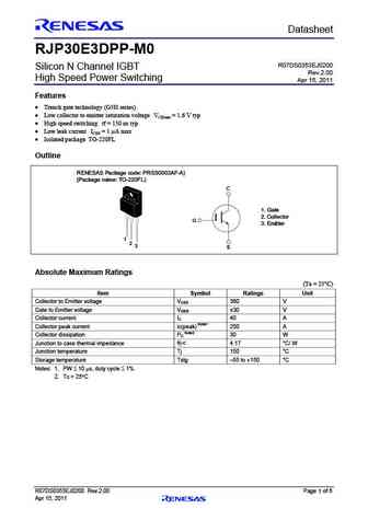
Preliminary Datasheet RJP30E3DPP-M0 R07DS0353EJ0200 Silicon N Channel IGBT Rev.2.00 High Speed Power Switching Apr 15, 2011 Features Trench gate technology (G5H series) Low collector to emitter saturation voltage VCE(sat) = 1.6 V typ High speed switching tf = 150 ns typ Low leak current ICES = 1 A max Isolated package TO-220FL Outline RENESAS Pack
np30n04quk.pdf
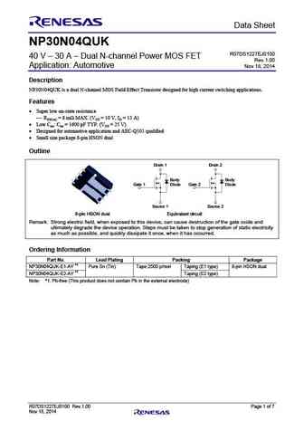
Data Sheet NP30N04QUK R07DS1227EJ0100 40 V 30 A Dual N-channel Power MOS FET Rev.1.00 Application Automotive Nov 18, 2014 Description NP30N04QUK is a dual N-channel MOS Field Effect Transistor designed for high current switching applications. Features Super low on-state resistance RDS(on) = 8 m MAX. (VGS = 10 V, ID = 15 A) Low Ciss Ciss = 1600 pF TYP.
r07ds0466ej rjp30h1dpp.pdf
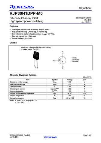
Preliminary Datasheet RJP30H1DPP-M0 R07DS0466EJ0200 Silicon N Channel IGBT Rev.2.00 High speed power switching Jun 15, 2011 Features Trench gate and thin wafer technology (G6H-II series) High speed switching tr =80 ns typ., tf = 150 ns typ. Low collector to emitter saturation voltage VCE(sat)= 1.5 V typ. Low leak current ICES = 1 A max. Isolated p
r07ds0465ej rjp30h1dpd.pdf
Preliminary Datasheet RJP30H1DPD R07DS0465EJ0200 Silicon N Channel IGBT Rev.2.00 High speed power switching Jun 15, 2011 Features Trench gate and thin wafer technology (G6H-II series) High speed switching tr = 80 ns typ., tf = 150 ns typ. Low collector to emitter saturation voltage VCE(sat) = 1.5 V typ. Low leak current ICES = 1 A max. Outline RENES
rjp30e3dpp-m0.pdf

Preliminary Datasheet RJP30E3DPP-M0 R07DS0353EJ0200 Silicon N Channel IGBT Rev.2.00 High Speed Power Switching Apr 15, 2011 Features Trench gate technology (G5H series) Low collector to emitter saturation voltage VCE(sat) = 1.6 V typ High speed switching tf = 150 ns typ Low leak current ICES = 1 A max Isolated package TO-220FL Outline RENESAS Pack
rjp30h1dpp-m0.pdf

Preliminary Datasheet RJP30H1DPP-M0 R07DS0466EJ0200 Silicon N Channel IGBT Rev.2.00 High speed power switching Jun 15, 2011 Features Trench gate and thin wafer technology (G6H-II series) High speed switching tr =80 ns typ., tf = 150 ns typ. Low collector to emitter saturation voltage VCE(sat)= 1.5 V typ. Low leak current ICES = 1 A max. Isolated p
rjp30h2dpk-m0 rjp30h2a.pdf
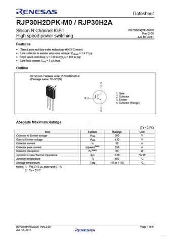
Preliminary Datasheet RJP30H2DPK-M0 / RJP30H2A R07DS0467EJ0200 Silicon N Channel IGBT Rev.2.00 High speed power switching Jun 15, 2011 Features Trench gate and thin wafer technology (G6H-II series) Low collector to emitter saturation voltage VCE(sat) = 1.4 V typ High speed switching tf = 100 ns typ, tf = 180 ns typ Low leak current ICES = 1 A max Outline
rjp30h2dpk-m0.pdf
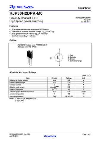
Preliminary Datasheet RJP30H2DPK-M0 R07DS0467EJ0200 Silicon N Channel IGBT Rev.2.00 High speed power switching Jun 15, 2011 Features Trench gate and thin wafer technology (G6H-II series) Low collector to emitter saturation voltage VCE(sat) = 1.4 V typ High speed switching tf = 100 ns typ, tf = 180 ns typ Low leak current ICES = 1 A max Outline RENES
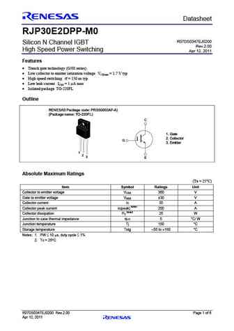
rjp30e2dpp-m0.pdf

Preliminary Datasheet RJP30E2DPP-M0 R07DS0347EJ0200 Silicon N Channel IGBT Rev.2.00 High Speed Power Switching Apr 12, 2011 Features Trench gate technology (G5H series) Low collector to emitter saturation voltage VCE(sat) = 1.7 V typ High speed switching tf = 150 ns typ Low leak current ICES = 1 A max Isolated package TO-220FL Outline RENESAS Pack
rjp30e2dpp rjh30e2 equivalent no diode.pdf
Preliminary Datasheet RJP30E2DPP-M0 R07DS0347EJ0200 Silicon N Channel IGBT Rev.2.00 High Speed Power Switching Apr 12, 2011 Features Trench gate technology (G5H series) Low collector to emitter saturation voltage VCE(sat) = 1.7 V typ High speed switching tf = 150 ns typ Low leak current ICES = 1 A max Isolated package TO-220FL Outline RENESAS Pack
r07ds0347ej rjp30e2dpp.pdf

Preliminary Datasheet RJP30E2DPP-M0 R07DS0347EJ0200 Silicon N Channel IGBT Rev.2.00 High Speed Power Switching Apr 12, 2011 Features Trench gate technology (G5H series) Low collector to emitter saturation voltage VCE(sat) = 1.7 V typ High speed switching tf = 150 ns typ Low leak current ICES = 1 A max Isolated package TO-220FL Outline RENESAS Pack
rfd3055le rfd3055lesm rfp3055le.pdf
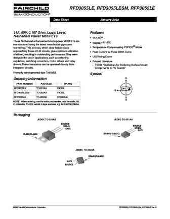
RFD3055LE, RFD3055LESM, RFP3055LE Data Sheet January 2002 11A, 60V, 0.107 Ohm, Logic Level, Features N-Channel Power MOSFETs 11A, 60V These N-Channel enhancement-mode power MOSFETs are rDS(ON) = 0.107 manufactured using the latest manufacturing process Temperature Compensating PSPICE Model technology. This process, which uses feature sizes approaching those of LSI
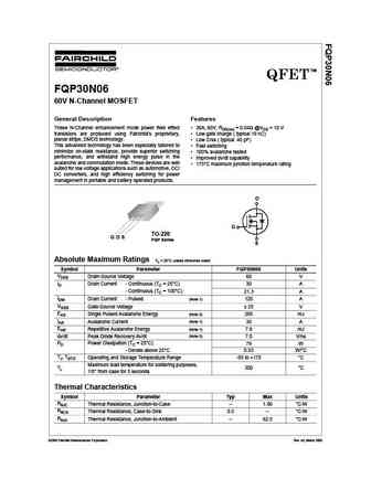
fqp30n06l.pdf
May 2001 TM QFET FQP30N06L 60V LOGIC N-Channel MOSFET General Description Features These N-Channel enhancement mode power field effect 32A, 60V, RDS(on) = 0.035 @VGS = 10 V transistors are produced using Fairchild s proprietary, Low gate charge ( typical 15 nC) planar stripe, DMOS technology. Low Crss ( typical 50 pF) This advanced technology has been especially tailo
rfp30n06le rf1s30n06lesm.pdf
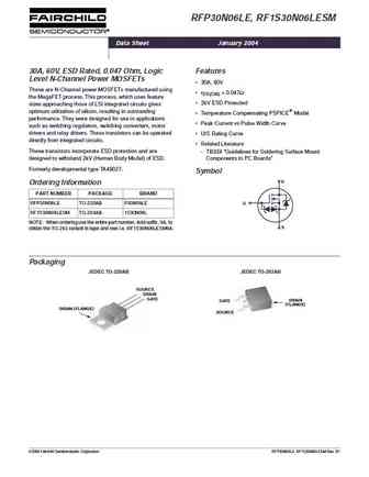
RFP30N06LE, RF1S30N06LESM Data Sheet January 2004 30A, 60V, ESD Rated, 0.047 Ohm, Logic Features Level N-Channel Power MOSFETs 30A, 60V These are N-Channel power MOSFETs manufactured using rDS(ON) = 0.047 the MegaFET process. This process, which uses feature 2kV ESD Protected sizes approaching those of LSI integrated circuits gives optimum utilization of silicon, res
rfg30p05 rfp30p05 rf1s30p05sm.pdf

RFG30P05, RFP30P05, RF1S30P05SM Data Sheet January 2002 30A, 50V, 0.065 Ohm, P-Channel Power Features MOSFETs 30A, 50V These are P-Channel power MOSFETs manufactured rDS(ON) = 0.065 using the MegaFET process. This process, which uses Temperature Compensating PSPICE Model feature sizes approaching those of LSI circuits, gives optimum utilization of silicon, resultin
tip30 tip30a tip30b tip30c.pdf
July 2008 TIP30/TIP30A/TIP30B/TIP30C PNP Epitaxial Silicon Transistor Features Complementary to TIP29/TIP29A/TIP29B/TIP29C 1. Base 2. Collector 3. Emitter Absolute Maximum Ratings TC=25 C unless otherwise noted Symbol Parameter Value Units VCBO Collector-Base Voltage TIP30 - 40 V TIP30A - 60 V TIP30B - 80 V TIP30C - 100 V VCEO Collector-Emitter Voltage TIP30 - 40
mtp3055vl.pdf
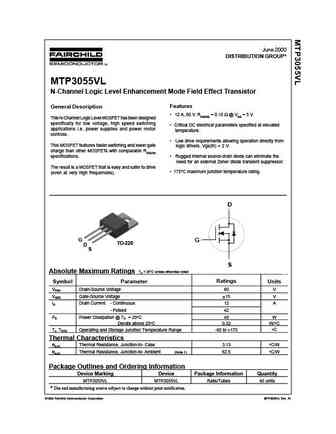
June 2000 DISTRIBUTION GROUP* MTP3055VL N-Channel Logic Level Enhancement Mode Field Effect Transistor Features General Description 12 A, 60 V. RDS(ON) = 0.18 @ VGS = 5 V This N-Channel Logic Level MOSFET has been designed specifically for low voltage, high speed switching Critical DC electrical parameters specified at elevated applications i.e. power supplies and power mo
fqp30n06.pdf
TM QFET FQP30N06 60V N-Channel MOSFET General Description Features These N-Channel enhancement mode power field effect 30A, 60V, RDS(on) = 0.04 @VGS = 10 V transistors are produced using Fairchild s proprietary, Low gate charge ( typical 19 nC) planar stripe, DMOS technology. Low Crss ( typical 40 pF) This advanced technology has been especially tailored to Fast s
rfg30p06 rfp30p06 rf1s30p06sm.pdf
RFG30P06, RFP30P06, RF1S30P06SM Data Sheet January 2002 30A, 60V, 0.065 Ohm, P-Channel Power Features MOSFETs 30A, 60V These are P-Channel power MOSFETs manufactured using rDS(ON) = 0.065 the MegaFET process. This process, which uses feature Temperature Compensating PSPICE Model sizes approaching those of LSI circuits, gives optimum utilization of silicon, resultin
tip30.pdf
TIP30 SERIES (TIP30/30A/30B/30C) PNP EPITAXIAL SILICON TRANSISTOR MEDIUM POWER LINEAR TO-220 SWITCHING APPLICATIONS Complement to TIP29/29A/29B/29C ABSOLUTE MAXIMUM RATINGS Characteristic Symbol Rating Unit Collector Emitter Voltage TIP30 VCBO - 40 V TIP30A - 60 V TIP30B - 80 V TIP30C - 100 V Collector Emitter Voltage TIP30 VCEO - 40 V TIP30A - 60 V TIP30B
bsp300.pdf
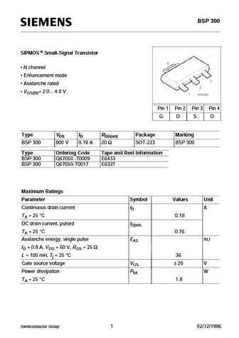
BSP 300 SIPMOS Small-Signal Transistor N channel Enhancement mode Avalanche rated VGS(th)= 2.0... 4.0 V Pin 1 Pin 2 Pin 3 Pin 4 G D S D Type VDS ID RDS(on) Package Marking BSP 300 800 V 0.19 A 20 SOT-223 BSP 300 Type Ordering Code Tape and Reel Information BSP 300 Q67050 -T0009 E6433 BSP 300 Q67050-T0017 E6327 Maximum Ratings Parameter Symbol Values Unit Co
bup304.pdf

BUP 304 IGBT Preliminary data Low forward voltage drop High switching speed Low tail current Latch-up free Avalanche rated Pin 1 Pin 2 Pin 3 G C E Type VCE IC Package Ordering Code BUP 304 1000V 35A TO-218 AB Q67078-A4200-A2 Maximum Ratings Parameter Symbol Values Unit Collector-emitter voltage VCE 1000 V Collector-gate voltage VCGR RGE = 20 k 1000 Gate-
bup306d.pdf
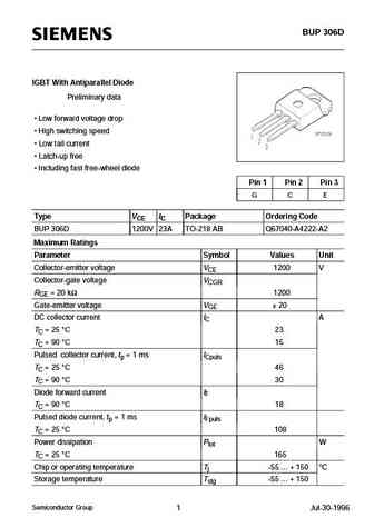
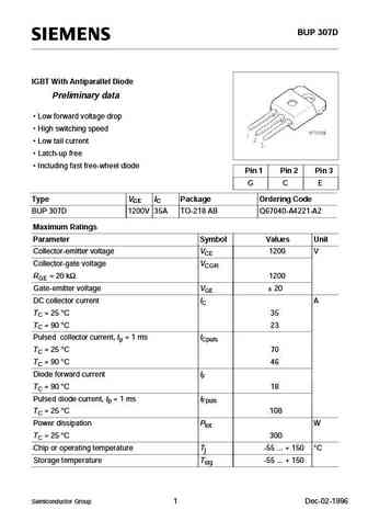
BUP 306D IGBT With Antiparallel Diode Preliminary data Low forward voltage drop High switching speed Low tail current Latch-up free Including fast free-wheel diode Pin 1 Pin 2 Pin 3 G C E Type VCE IC Package Ordering Code BUP 306D 1200V 23A TO-218 AB Q67040-A4222-A2 Maximum Ratings Parameter Symbol Values Unit Collector-emitter voltage VCE 1200 V Collector-ga
bup305d.pdf
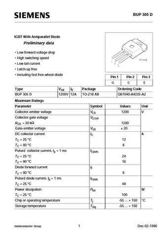
BUP 305 D IGBT With Antiparallel Diode Preliminary data Low forward voltage drop High switching speed Low tail current Latch-up free Including fast free-wheel diode Pin 1 Pin 2 Pin 3 G C E Type VCE IC Package Ordering Code BUP 305 D 1200V 12A TO-218 AB Q67040-A4225-A2 Maximum Ratings Parameter Symbol Values Unit Collector-emitter voltage VCE 1200 V Collector-
bup302.pdf
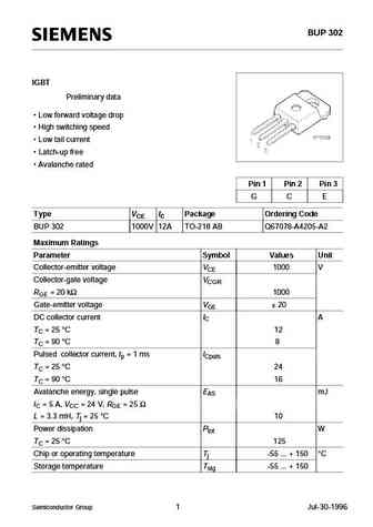
BUP 302 IGBT Preliminary data Low forward voltage drop High switching speed Low tail current Latch-up free Avalanche rated Pin 1 Pin 2 Pin 3 G C E Type VCE IC Package Ordering Code BUP 302 1000V 12A TO-218 AB Q67078-A4205-A2 Maximum Ratings Parameter Symbol Values Unit Collector-emitter voltage VCE 1000 V Collector-gate voltage VCGR RGE = 20 k 1000 Gate-
bup307.pdf
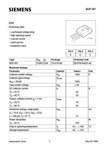
BUP 307 IGBT Preliminary data Low forward voltage drop High switching speed Low tail current Latch-up free Avalanche rated Pin 1 Pin 2 Pin 3 G C E Type VCE IC Package Ordering Code BUP 307 1200V 35A TO-218 AB Q67078-A4201-A2 Maximum Ratings Parameter Symbol Values Unit Collector-emitter voltage VCE 1200 V Collector-gate voltage VCGR RGE = 20 k 1200 Gate-
bup309.pdf
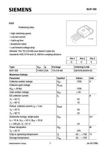
BUP 309 IGBT Preliminary data High switching speed Low tail current Latch-up free Avalanche rated Low forward voltage drop Remark The TO-218 AB case doesn't solve the standards VDE 0110 and UL 508 for creeping distance Pin 1 Pin 2 Pin 3 G C E Type VCE IC Package Ordering Code BUP 309 1700V 25A TO-218 AB Q67078-A4204-A2 Maximum Ratings Parameter Symbol Values
bup300.pdf
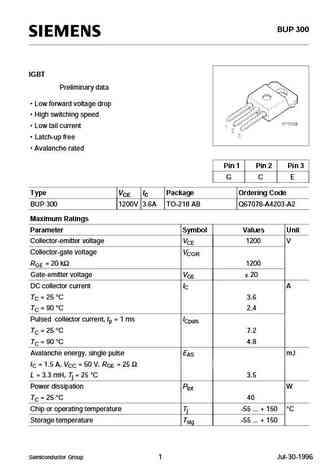
BUP 300 IGBT Preliminary data Low forward voltage drop High switching speed Low tail current Latch-up free Avalanche rated Pin 1 Pin 2 Pin 3 G C E Type VCE IC Package Ordering Code BUP 300 1200V 3.6A TO-218 AB Q67078-A4203-A2 Maximum Ratings Parameter Symbol Values Unit Collector-emitter voltage VCE 1200 V Collector-gate voltage VCGR RGE = 20 k 1200 Gate
byp303.pdf

BYP 303 FRED Diode Fast recovery epitaxial diode Soft recovery characteristics Type VRRM IFRMS trr Package Ordering Code BYP 303 1200V 65A 140ns TO-218 AD C67047-A2253-A2 Maximum Ratings Parameter Symbol Values Unit Mean forward current IFAV A TC = 90 C, D = 0.5 40 RMS forward current IFRMS 65 Surge forward current, sine halfwave, aperiodic IFSM Tj = 100 C, f = 50 Hz 170
byp302.pdf
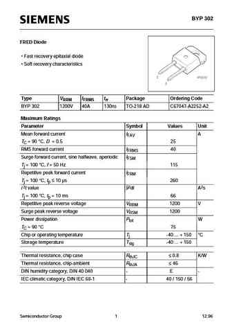
BYP 302 FRED Diode Fast recovery epitaxial diode Soft recovery characteristics Type VRRM IFRMS trr Package Ordering Code BYP 302 1200V 40A 130ns TO-218 AD C67047-A2252-A2 Maximum Ratings Parameter Symbol Values Unit Mean forward current IFAV A TC = 90 C, D = 0.5 25 RMS forward current IFRMS 40 Surge forward current, sine halfwave, aperiodic IFSM Tj = 100 C, f = 50 Hz 115
bup307d.pdf
BUP 307D IGBT With Antiparallel Diode Preliminary data Low forward voltage drop High switching speed Low tail current Latch-up free Including fast free-wheel diode Pin 1 Pin 2 Pin 3 G C E Type VCE IC Package Ordering Code BUP 307D 1200V 35A TO-218 AB Q67040-A4221-A2 Maximum Ratings Parameter Symbol Values Unit Collector-emitter voltage VCE 1200 V Collector-ga
bup303.pdf
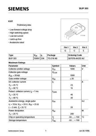
BUP 303 IGBT Preliminary data Low forward voltage drop High switching speed Low tail current Latch-up free Avalanche rated Pin 1 Pin 2 Pin 3 G C E Type VCE IC Package Ordering Code BUP 303 1000V 23A TO-218 AB Q67078-A4202-A2 Maximum Ratings Parameter Symbol Values Unit Collector-emitter voltage VCE 1000 V Collector-gate voltage VCGR RGE = 20 k 1000 Gate-
byp301.pdf
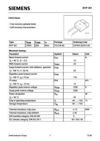
BYP 301 FRED Diode Fast recovery epitaxial diode Soft recovery characteristics Type VRRM IFRMS trr Package Ordering Code BYP 301 1200V 20A 80ns TO-218 AD C67047-A2251-A2 Maximum Ratings Parameter Symbol Values Unit Mean forward current IFAV A TC = 90 C, D = 0.5 12 RMS forward current IFRMS 20 Surge forward current, sine halfwave, aperiodic IFSM Tj = 100 C, f = 50 Hz 50
byp300.pdf

BYP 300 Preliminary data FRED Diode Fast recovery epitaxial diode Soft recovery characteristics Type VRRM IFRMS trr Package Ordering Code BYP 300 1200V 6.5A 55ns TO-218 AD C67047-A2250-A2 Maximum Ratings Parameter Symbol Values Unit Mean forward current IFAV A TC = 90 C, D = 0.5 4 RMS forward current IFRMS 6.5 Surge forward current, sine halfwave, aperiodic IFSM Tj = 100
tip30-a-b-c.pdf
145 Adams Avenue, Hauppauge, NY 11788 USA Tel (631) 435-1110 Fax (631) 435-1824
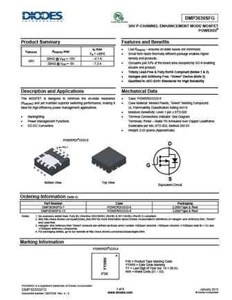
dmp3028lk3.pdf
DMP3028LK3 30V P-CHANNEL ENHANCEMENT MODE MOSFET Product Summary Features ID 100% Unclamped Inductive Switch (UIS) Test In Production V(BR)DSS RDS(on) TC = +25 C Low On-Resistance Fast Switching Speed 25m @ VGS = -10V -27A -30V Totally Lead-Free & Fully RoHS Compliant (Note 1 & 2) 38m @ VGS = -4.5V -22A Halogen and Antimony Free. Green Devi
dmp3037lss.pdf
DMP3037LSS P-CHANNEL ENHANCEMENT MODE MOSFET Product Summary Features Low On-Resistance ID V(BR)DSS RDS(on) max Low Input Capacitance TC = +25 C Fast Switching Speed 32m @ VGS = -10V -5.8A -30V Low Input/Output Leakage 50m @ VGS = -4.5V -4.6A Totally Lead-Free & Fully RoHS Compliant (Notes 1 & 2) Halogen and Antimony Free. Green Devi
dmp3015lss.pdf
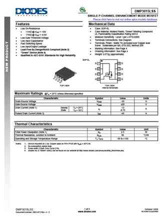
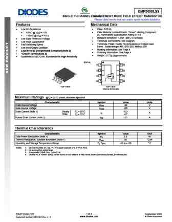
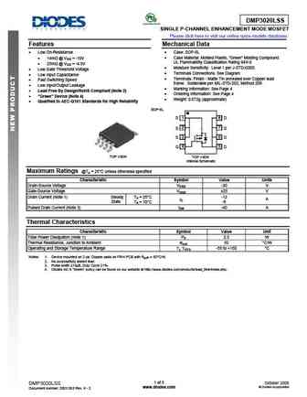
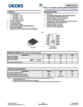
DMP3015LSS SINGLE P-CHANNEL ENHANCEMENT MODE MOSFET Please click here to visit our online spice models database. Features Mechanical Data Low On-Resistance Case SOP-8L 11m @ VGS = -10V Case Material Molded Plastic, Green Molding Compound. UL Flammability Classification Rating 94V-0 17m @ VGS = -4.5V Moisture Sensitivity Level 1 per J-STD-020D
dmp3030sn.pdf
DMP3030SN P-CHANNEL ENHANCEMENT MODE FIELD EFFECT TRANSISTOR Features Mechanical Data Low On-Resistance Case SC-59 Low Gate Threshold Voltage Case Material Molded Plastic, Green Molding Compound. UL Flammability Classification Rating 94V-0 Low Input Capacitance Moisture sensitivity Level 1 per J-STD-020C Fast Switching Speed Lead Free By
dmp3017sfgq.pdf
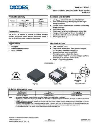
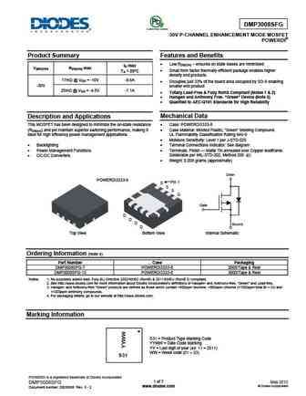
DMP3017SFGQ 30V P-CHANNEL ENHANCEMENT MODE MOSFET POWERDI Product Summary Features and Benefits ID Max Low RDS(ON) Ensures On-State Losses Are Minimized V(BR)DSS RDS(ON) Max TA = +25 C Small form factor thermally efficient package enables higher density end products 10m @ VGS = -10V -11.5A -30V Occupies just 33% of the board area occupied by SO-8 enab
dmp3012lps.pdf
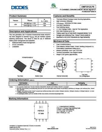
DMP3012LPS P-CHANNEL ENHANCEMENT MODE MOSFET POWERDI 5060-8 Product Summary Features and Benefits Thermally Efficient Package-Cooler Running Applications ID V(BR)DSS RDS(ON) TC = +25 C High Conversion Efficiency Low Minimizes On State Losses 9m @ VGS = -10V -45A RDS(ON) -30V Low Input Capacitance 12m @ VGS = -4.5V -35A Fast Switching Speed
dmp3010lps.pdf
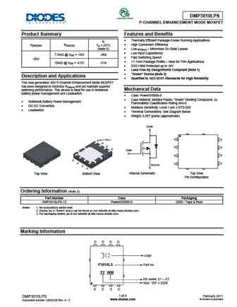
DMP3010LPS P-CHANNEL ENHANCEMENT MODE MOSFET Product Summary Features and Benefits Thermally Efficient Package-Cooler Running Applications ID High Conversion Efficiency V(BR)DSS RDS(ON) TA = 25 C (Note 5) Low Minimizes On State Losses RDS(on) Low Input Capacitance 7.5m @ VGS = -10V -36A Fast Switching Speed -30V
dmp3085lsd.pdf
DMP3085LSD P-CHANNEL ENHANCEMENT MODE MOSFET Product Summary Features ID Low On-Resistance V(BR)DSS RDS(ON) MAX Package TA = +25 C Low Input Capacitance 70m @VGS = -10V -3.9A Fast Switching Speed -30V SO-8 95m @VGS = -4.5V -3.3A Totally Lead-Free & Fully RoHS Compliant (Notes 1 & 2) Halogen and Antimony Free. Green Device (Note 3) Qua
dmp3010lpsq.pdf
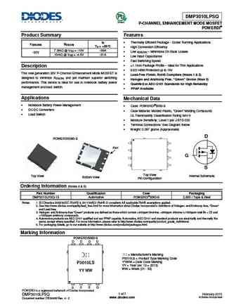
DMP3010LPSQ Green P-CHANNEL ENHANCEMENT MODE MOSFET POWERDI Product Summary Features ID Thermally Efficient Package - Cooler Running Applications V(BR)DSS RDS(ON) TA = +25 C High Conversion Efficiency 7.5m @ VGS = -10V -36A Low RDS(ON) Minimizes On State Losses -30V 10m @ VGS = -4.5V -31A Low Input Capacitance Fast Switching Speed
dmp3036ssd.pdf
DMP3036SSD P-CHANNEL ENHANCEMENT MODE MOSFET Product Summary Features ID Low On-Resistance V(BR)DSS RDS(on) max TC = +25 C Low Input Capacitance 20m @ VGS = -10V -18.0A -30V Fast Switching Speed -15.0A 29m @ VGS = -5V Totally Lead-Free & Fully RoHS Compliant (Notes 1 & 2) Halogen and Antimony Free. Green Device (Note 3) Description
dmp3056l.pdf
DMP3056L 30V P-CHANNEL ENHANCEMENT MODE MOSFET Product Summary Features Low On-Resistance ID MAX V(BR)DSS RDS(ON) Low Gate Threshold Voltage TA = +25 C Low Input Capacitance 50m @ VGS =-10V -4.3A -30V Fast Switching Speed 70m @ VGS =-4.5V -3.7A Low Input/Output Leakage Totally Lead-Free & Fully RoHS Compliant (Notes 1 & 2) Halogen
dmp3035sfg.pdf
DMP3035SFG 30V P-CHANNEL ENHANCEMENT MODE MOSFET POWERDI Product Summary Features and Benefits Low RDS(ON) ensures on state losses are minimized ID max V(BR)DSS RDS(ON) max Small form factor thermally efficient package enables higher TA = 25 C density end products 20m @ VGS = -10V -9.5 A Occupies just 33% of the board area occupied by SO-8 enabling -
dmp3065lvt.pdf
DMP3065LVT P-CHANNEL ENHANCEMENT MODE MOSFET Product Summary Features and Benefits ID max Low On-Resistance V(BR)DSS RDS(ON) max TA = +25 C Low Input Capacitance Fast Switching Speed 42m @ VGS = -10V -5.1A -30V ESD Protected Gate 65m @ VGS = -4.5V -4.0A Totally Lead-Free & Fully RoHS Compliant (Notes 1 & 2) Halogen and Antimony Free. Gre
dmp3098lss.pdf
DMP3098LSS SINGLE P-CHANNEL ENHANCEMENT MODE FIELD EFFECT TRANSISTOR Please click here to visit our online spice models database. Features Mechanical Data Low On-Resistance Case SOP-8L 65m @ VGS = -10V Case Material Molded Plastic, Green Molding Compound. UL Flammability Classification Rating 94V-0 115m @ VGS = -4.5V Moisture Sensitivity Leve
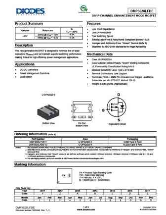
dmp3028lfde.pdf
DMP3028LFDE 30V P-CHANNEL ENHANCEMENT MODE MOSFET Product Summary Features ID Low Input Capacitance V(BR)DSS RDS(on) max TA = +25 C Low On-Resistance 25m @ VGS = -10V -6.8A -30V Fast Switching Speed -5.0A 38m @ VGS = -4.5V Totally Lead-Free & Fully RoHS Compliant (Notes 1 & 2) Halogen and Antimony Free. Green Device (Note 3) Descripti
dmp3008sfg.pdf
DMP3008SFG 30V P-CHANNEL ENHANCEMENT MODE MOSFET POWERDI Product Summary Features and Benefits Low RDS(ON) ensures on state losses are minimized ID max V(BR)DSS RDS(ON) max Small form factor thermally efficient package enables higher TA = 25 C density end products 17m @ VGS = -10V -8.6A Occupies just 33% of the board area occupied by SO-8 enabling -3
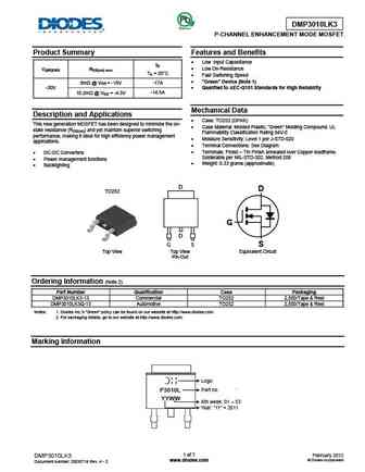
dmp3010lk3.pdf
DMP3010LK3 P-CHANNEL ENHANCEMENT MODE MOSFET Product Summary Features and Benefits Low Input Capacitance ID Low On-Resistance V(BR)DSS RDS(on) max TA = 25 C Fast Switching Speed "Green" Device (Note 1) 8m @ VGS = -10V -17A -30V Qualified to AEC-Q101 Standards for High Reliability 10.2m @ VGS = -4.5V -14.5A Mechanical Data Description and Appl
dmp3017sfk.pdf
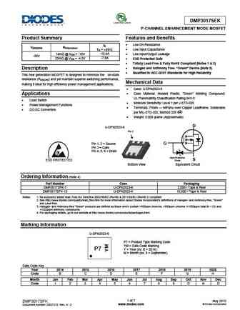
DMP3017SFK P-CHANNEL ENHANCEMENT MODE MOSFET Product Summary Features and Benefits Low On-Resistance ID V(BR)DSS RDS(on)max Low Input Capacitance TA = +25 C 14m @ VGS = -10V -10.4A Low Input/Output Leakage -30V 25m @ VGS = -4.5V -7.8A ESD Protected Gate Totally Lead-Free & Fully RoHS Compliant (Notes 1 & 2) Halogen and Antimony Free.
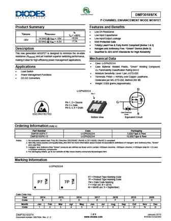
dmp3007sps.pdf
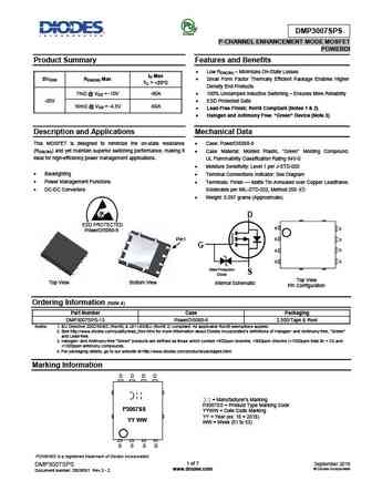
DMP3007SPS Green P-CHANNEL ENHANCEMENT MODE MOSFET POWERDI Product Summary Features and Benefits Low RDS(ON) Minimizes On-State Losses ID Max BVDSS RDS(ON) Max Small Form Factor Thermally Efficient Package Enables Higher TC = +25 C Density End Products 7m @ VGS = -10V -90A 100% Unclamped Inductive Switching Ensures More Reliability -30V ESD Pro
dmp3056ldm.pdf
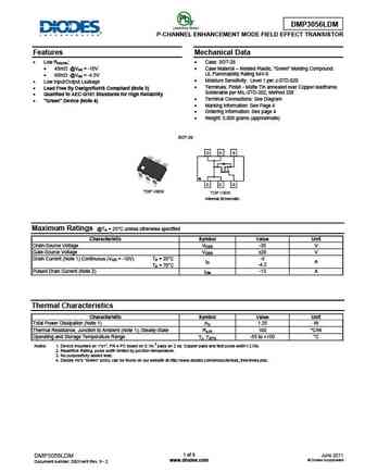
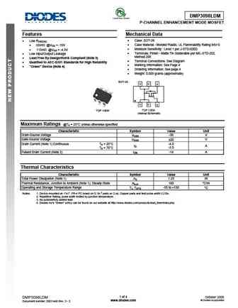
DMP3056LDM P-CHANNEL ENHANCEMENT MODE FIELD EFFECT TRANSISTOR Features Mechanical Data Low RDS(ON) Case SOT-26 45m @VGS = -10V Case Material Molded Plastic, Green Molding Compound. UL Flammability Rating 94V-0 65m @VGS = -4.5V Moisture Sensitivity Level 1 per J-STD-020 Low Input/Output Leakage Terminals Finish - Matte Tin anneale
dmp3098lq.pdf
DMP3098LQ P-CHANNEL ENHANCEMENT MODE MOSFET Product Summary Features and Benefits Low On-Resistance ID V(BR)DSS RDS(on) max Low Gate Threshold Voltage TA = +25 C 70m @ VGS = -10V -3.8A Low Input Capacitance -30V 120m @ VGS = -4.5V -3.0A Fast Switching Speed Low Input/Output Leakage Totally Lead-Free & Fully RoHS Compliant (Notes 1 & 2) H
dmp3050lvt.pdf
DMP3050LVT P-CHANNEL ENHANCEMENT MODE MOSFET Product Summary Features Low On-Resistance ID max V(BR)DSS RDS(ON) max Low Input Capacitance TA = 25 C Fast Switching Speed 50m @ VGS = -10V -4.5A Totally Lead-Free & Fully RoHS Compliant (Notes 1 & 2) -30V 90m @ VGS = -4.5V -3.5A Halogen and Antimony Free. Green Device (Note 3) Qualified
dmp3007scg.pdf
DMP3007SCG 30V P-CHANNEL ENHANCEMENT MODE MOSFET Product Summary Features and Benefits ID Max Low RDS(ON) Ensures On State Losses are Minimized BVDSS RDS(ON) Max TC = +25 C Small Form Factor Thermally Efficient Package Enables Higher Density End Products 6.8m @ VGS = -10V -50A -30V Occupies Just 33% of the Board Area Occupied by SO-8 Enabling 13m @
dmp3085lss.pdf
DMP3085LSS P-CHANNEL ENHANCEMENT MODE MOSFET Product Summary Features ID Low On-Resistance V(BR)DSS RDS(ON) MAX Package TA = +25 C Low Input Capacitance 70m @VGS = -10V -3.8A Fast Switching Speed -30V SO-8 95m @VGS = -4.5V -3.2A Totally Lead-Free & Fully RoHS Compliant (Notes 1 & 2) Halogen and Antimony Free. Green Device (Note 3) Qua
dmp3020lss.pdf
DMP3020LSS SINGLE P-CHANNEL ENHANCEMENT MODE MOSFET Please click here to visit our online spice models database. Features Mechanical Data Low On-Resistance Case SOP-8L 14m @ VGS = -10V Case Material Molded Plastic, Green Molding Compound. UL Flammability Classification Rating 94V-0 25m @ VGS = -4.5V Moisture Sensitivity Level 1 per J-STD-020D
dmp3036sfg.pdf
DMP3036SFG 30V P-CHANNEL ENHANCEMENT MODE MOSFET POWERDI Product Summary Features and Benefits ID max Low RDS(ON) ensures on state losses are minimized. V(BR)DSS RDS(ON) max TA = +25 C Small form factor thermally efficient package enables higher density end products. 20m @ VGS = -10V - 8.7 A -30V Occupies just 33% of the board area occupied by SO-8 enab
dmp3098lsd.pdf
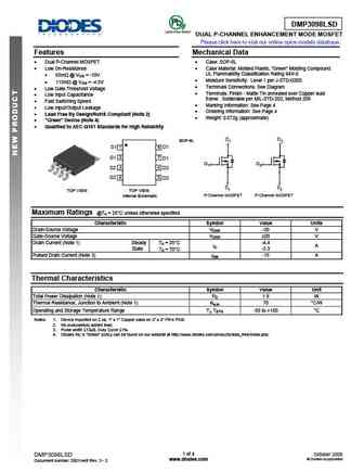
DMP3098LSD DUAL P-CHANNEL ENHANCEMENT MODE MOSFET Please click here to visit our online spice models database. Features Mechanical Data Dual P-Channel MOSFET Case SOP-8L Low On-Resistance Case Material Molded Plastic, Green Molding Compound. UL Flammability Classification Rating 94V-0 65m @ VGS = -10V Moisture Sensitivity Level 1 per J-STD-020D
dmp3098ldm.pdf
DMP3098LDM P-CHANNEL ENHANCEMENT MODE MOSFET Features Mechanical Data Low RDS(ON) Case SOT-26 Case Material - Molded Plastic. UL Flammability Rating 94V-0 65m @VGS = -10V Moisture Sensitivity Level 1 per J-STD-020D 115m @VGS = -4.5V Terminals Finish - Matte Tin Solderable per MIL-STD-202, Low Input/Output Leakage Method 208 Lead F
dmp3050lss.pdf
DMP3050LSS P-CHANNEL ENHANCEMENT MODE MOSFET Product Summary Features Low On-Resistance ID max V(BR)DSS RDS(ON) max Low Input Capacitance TA = 25 C Fast Switching Speed 45m @ VGS = -10V -4.8A Totally Lead-Free & Fully RoHS Compliant (Notes 1 & 2) -30V 80m @ VGS = -4.5V -3.5A Halogen and Antimony Free. Green Device (Note 3) Qualified
dmp3056lss.pdf
DMP3056LSS SINGLE P-CHANNEL ENHANCEMENT MODE FIELD EFFECT TRANSISTOR Please click here to visit our online spice models database. Features Mechanical Data Low On-Resistance Case SOP-8L 45m @ VGS = -10V Case Material Molded Plastic, Green Molding Compound. UL Flammability Classification Rating 94V-0 65m @ VGS = -4.5V Moisture Sensitivity Level
dmp3056lsd.pdf
DMP3056LSD DUAL P-CHANNEL ENHANCEMENT MODE FIELD EFFECT TRANSISTOR Please click here to visit our online spice models database. Features Mechanical Data Dual P-Channel MOSFET Case SOP-8L Low On-Resistance Case Material Molded Plastic, Green Molding Compound. UL Flammability Classification Rating 94V-0 45m @ VGS = -10V Moisture Sensitivity Level
dmp3028lsd.pdf
DMP3028LSD Maximum Ratings (@TA = +25 C, unless otherwise specified.) Characteristic Symbol Value Units Drain-Source Voltage VDSS -30 V Gate-Source Voltage 20 V VGSS Steady TA = +25 C -6 ID A State -4.7 TA = +70 C Continuous Drain Current (Note 5) VGS = 10V TA = +25 C -7.4 t
dmp3098l.pdf
DMP3098L P-CHANNEL ENHANCEMENT MODE MOSFET Features Mechanical Data Low On-Resistance Case SOT-23 70m @ VGS = -10V, ID = -3.8A Case Material Molded Plastic, Green Molding Compound. UL Flammability Classification Rating 94V-0 120m @ VGS = -4.5V, ID = -3.0A Moisture Sensitivity Level 1 per J-STD-020 Low Gate Threshold Voltage Terminals Fi
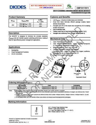
dmp3013sfv.pdf

DMP3013SFV 30V P-CHANNEL ENHANCEMENT MODE MOSFET PowerDI3333-8 (Type UX) Product Summary Features and Benefits ID max Low RDS(ON) Ensures On-State Losses are Minimized BVDSS RDS(ON) max TC = +25 C Small form Factor Thermally Efficient Package Enables Higher Density End Products 9.5m @ VGS = -10V -35A -30V Occupies 33% of the Board Area Occupied by SO-8 En
dmp3068l.pdf
DMP3068L 30V P-CHANNEL ENHANCEMENT MODE MOSFET Product Summary Features Low On-Resistance V(BR)DS ID max Low Gate Threshold Voltage RDS(ON) max Package TA = +25 C S Low Input Capacitance Fast Switching Speed -3.9A 72m @ VGS = -10V Low Input/Output Leakage -30V SOT-23 85m @ VGS = -4.5V -3.6A Totally Lead-Free & Fully RoHS Compliant (
dmp3017sfg.pdf
DMP3017SFG 30V P-CHANNEL ENHANCEMENT MODE MOSFET POWERDI Product Summary Features and Benefits ID max Low RDS(ON) ensures on state losses are minimized V(BR)DSS RDS(ON) max TA = +25 C Small form factor thermally efficient package enables higher density end products 10m @ VGS = -10V -11.5A -30V Occupies just 33% of the board area occupied by SO-8 enabli
dmp3099l.pdf
DMP3099L P-CHANNEL ENHANCEMENT MODE MOSFET Product Summary Features and Benefits ID max Low Gate Threshold Voltage V(BR)DSS RDS(ON) max TA = +25 C Low Input Capacitance Fast Switching Speed 65m @ VGS = -10V -3.8A -30V Low Input/Output Leakage 99m @ VGS = -4.5V -3.0A Totally Lead-Free & Fully RoHS compliant (Notes 1 & 2) Halogen and Antimony
dmp3036sfv.pdf
DMP3036SFV 30V P-CHANNEL ENHANCEMENT MODE MOSFET PowerDI3333-8 (Type UX) Product Summary Features Low RDS(ON) Ensures On State Losses Are Minimized ID Max BVDSS RDS(ON) Max Small Form Factor Thermally Efficient Package Enables Higher TC = +25 C Density End Products 20m @ VGS = -10V Occupies Just 33% of The Board Area Occupied by SO-8 -30V -30A 29m
bsp300.pdf
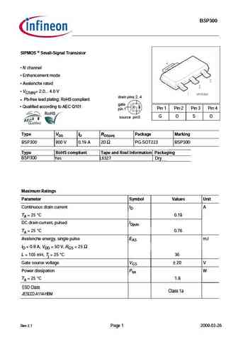
BSP300 SIPMOS Small-Signal Transistor N channel Enhancement mode Avalanche rated VGS(th)= 2.0... 4.0 V Pb-free lead plating; RoHS compliant Qualified according to AEC Q101 Pin 1 Pin 2 Pin 3 Pin 4 G D S D Type VDS ID RDS(on) Package Marking BSP300 800 V 0.19 A 20 PG-SOT223 BSP300 Type RoHS compliant Tape and Reel Information Packaging BSP300 Yes L632
fp30r06w1e3.pdf
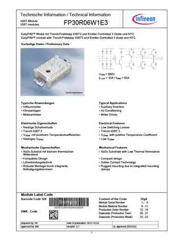
Technische Information / Technical Information IGBT-Module FP30R06W1E3 IGBT-modules EasyPIM Modul mit Trench/Feldstopp IGBT3 und Emitter Controlled 3 Diode und NTC EasyPIM module with Trench/Fieldstop IGBT3 and Emitter Controlled 3 diode and NTC Vorl ufige Daten / Preliminary Data V = 600V CES I = 30A / I = 60A C nom CRM Typische Anwendungen Typical Applications Hilfsumri
bsp3081.pdf
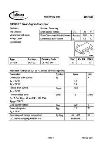
Preliminary data BSP308 SIPMOS Small-Signal-Transistor Features Product Summary N-Channel Drain source voltage VDS 30 V Enhancement mode Drain-Source on-state resistance RDS(on) 0.05 Logic Level Continuous drain current ID 4.7 A dv/dt rated 4 3 2 1 VPS05163 Type Package Ordering Code Pin 1 Pin 2/4 PIN 3 BSP308 SOT-223 Q67000-S4011 G D S Maximum Ratings,a
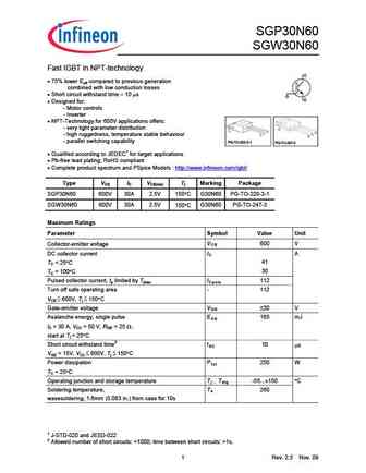
sgp30n60 sgw30n60 rev2 5g.pdf

SGP30N60 SGW30N60 Fast IGBT in NPT-technology C 75% lower Eoff compared to previous generation combined with low conduction losses Short circuit withstand time 10 s G E Designed for - Motor controls - Inverter NPT-Technology for 600V applications offers - very tight parameter distribution - high ruggedness, temperature stable behaviour - paral
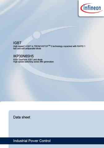
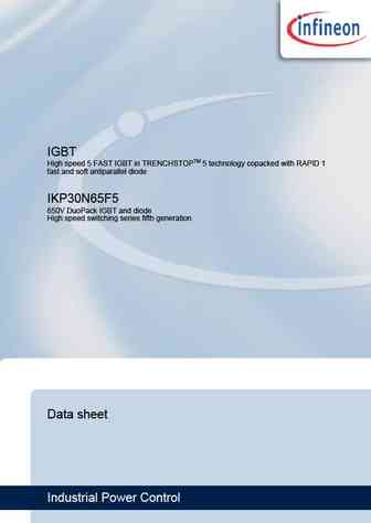
ikp30n65h5.pdf
IGBT High speed 5 IGBT in TRENCHSTOPTM 5 technology copacked with RAPID 1 fast and soft antiparallel diode IKP30N65H5 650V DuoPack IGBT and diode High speed switching series fifth generation Data sheet Industrial Power Control IKP30N65H5 High speed switching series fifth generation High speed 5 IGBT in TRENCHSTOPTM 5 technology copacked with RAPID 1 fast and soft antiparallel diode
sgp30n60 sgw30n60 rev2.pdf
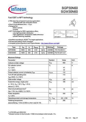
SGP30N60 SGW30N60 Fast IGBT in NPT-technology C 75% lower Eoff compared to previous generation combined with low conduction losses Short circuit withstand time 10 s G E Designed for - Motor controls - Inverter NPT-Technology for 600V applications offers - very tight parameter distribution - high ruggedness, temperature stable behaviour - paral
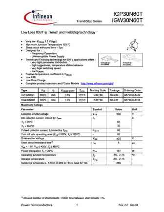
igp30n60t.pdf
IGP30N60T TrenchStop Series IGW30N60T Low Loss IGBT in Trench and Fieldstop technology C Very low VCE(sat) 1.5 V (typ.) Maximum Junction Temperature 175 C Short circuit withstand time 5 s G Designed for E - Frequency Converters - Uninterruptible Power Supply Trench and Fieldstop technology for 600 V applications offers - very tight paramete
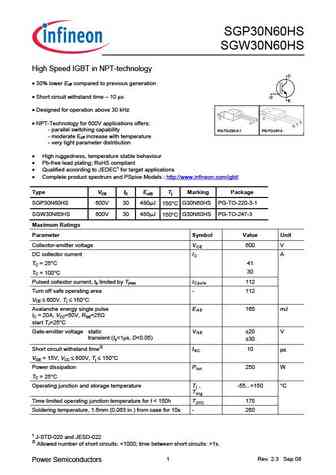
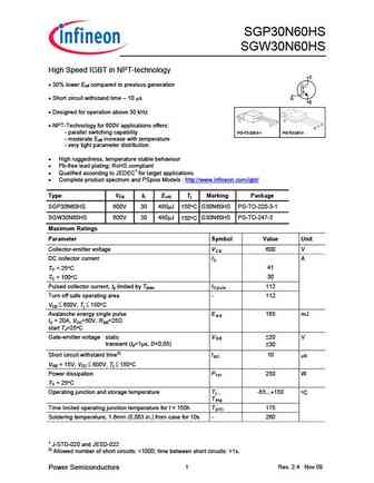
sgp30n60hs.pdf

SGP30N60HS SGW30N60HS High Speed IGBT in NPT-technology C 30% lower Eoff compared to previous generation Short circuit withstand time 10 s G E Designed for operation above 30 kHz NPT-Technology for 600V applications offers - parallel switching capability PG-TO-220-3-1 PG-TO-247-3 - moderate Eoff increase with temperature - very tight parameter distribut
igp30n60h3.pdf

IGBT High speed IGBT in Trench and Fieldstop technology IGP30N60H3 600V high speed switching series third generation Data sheet Industrial Power Control IGP30N60H3 High speed switching series third generation High speed IGBT in Trench and Fieldstop technology Features C TRENCHSTOPTM technology offering very low turn-off energy low V CEsat low EMI maximum junctio
igp30n65f5.pdf
IGBT High speed 5 FAST IGBT in TRENCHSTOPTM 5 technology IGP30N65F5 650V IGBT high speed switching series fifth generation Data sheet Industrial Power Control IGP30N65F5 High speed switching series fifth generation High speed 5 FAST IGBT in TRENCHSTOPTM 5 technology Features and Benefits C High speed F5 technology offering Best-in-Class efficiency in hard switching and resonant
igp30n60h3 rev1 2g.pdf
IGBT High speed IGBT in Trench and Fieldstop technology IGP30N60H3 600V high speed switching series third generation Datasheet Industrial & Multimarket IGP30N60H3 High speed switching series third generation High speed IGBT in Trench and Fieldstop technology Features C TRENCHSTOPTM technology offering very low V CEsat low EMI maximum junction temperature 175 C G
sgp30n60hs sgw30n60hs rev2.pdf
SGP30N60HS SGW30N60HS High Speed IGBT in NPT-technology C 30% lower Eoff compared to previous generation Short circuit withstand time 10 s G E Designed for operation above 30 kHz NPT-Technology for 600V applications offers - parallel switching capability PG-TO-220-3-1 PG-TO-247-3 - moderate Eoff increase with temperature - very tight parameter distribut
sgp30n60.pdf
SGP30N60 SGW30N60 Fast IGBT in NPT-technology C 75% lower Eoff compared to previous generation combined with low conduction losses Short circuit withstand time 10 s G E Designed for - Motor controls - Inverter NPT-Technology for 600V applications offers - very tight parameter distribution - high ruggedness, temperature stable behaviour - paral
sgp30n60hs sgw30n60hs rev2 4g.pdf
SGP30N60HS SGW30N60HS High Speed IGBT in NPT-technology C 30% lower Eoff compared to previous generation Short circuit withstand time 10 s G E Designed for operation above 30 kHz NPT-Technology for 600V applications offers - parallel switching capability PG-TO-220-3-1 PG-TO-247-3 - moderate Eoff increase with temperature - very tight parameter distribut
sgp30n60 sgw30n60.pdf
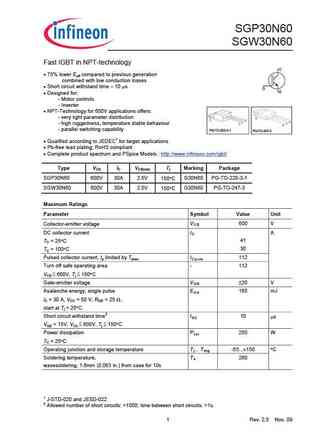
SGP30N60 SGW30N60 Fast IGBT in NPT-technology C 75% lower Eoff compared to previous generation combined with low conduction losses Short circuit withstand time 10 s G E Designed for - Motor controls - Inverter NPT-Technology for 600V applications offers - very tight parameter distribution - high ruggedness, temperature stable behaviour - parallel switc
fp30r06w1e3-b11.pdf
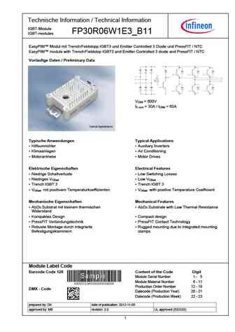
Technische Information / Technical Information IGBT-Module FP30R06W1E3_B11 IGBT-modules EasyPIM Modul mit Trench/Feldstopp IGBT3 und Emitter Controlled 3 Diode und PressFIT / NTC EasyPIM module with Trench/Fieldstop IGBT3 and Emitter Controlled 3 diode and PressFIT / NTC Vorl ufige Daten / Preliminary Data V = 600V CES I = 30A / I = 60A C nom CRM Typische Anwendungen Typical A
igp30n65h5.pdf

IGBT High speed 5 IGBT in TRENCHSTOPTM 5 technology IGP30N65H5 650V IGBT high speed switching series fifth generation Data sheet Industrial Power Control IGP30N65H5 High speed switching series fifth generation High speed 5 IGBT in TRENCHSTOPTM 5 technology Features and Benefits C High speed H5 technology offering Best-in-Class efficiency in hard switching and resonant topologi
bsp308.pdf
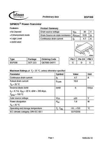
Preliminary data BSP308 SIPMOS Power-Transistor Features Product Summary N-Channel Drain source voltage VDS 30 V Enhancement mode Drain-Source on-state resistance RDS(on) 0.05 Logic Level Continuous drain current ID 4.7 A dv/dt rated 4 3 2 1 VPS05163 Type Package Ordering Code Pin 1 Pin 2/4 PIN 3 BSP308 SOT-223 Q67000-S4011 G D S Maximum Ratings,at Tj =
ikp30n65f5.pdf
IGBT High speed 5 FAST IGBT in TRENCHSTOPTM 5 technology copacked with RAPID 1 fast and soft antiparallel diode IKP30N65F5 650V DuoPack IGBT and diode High speed switching series fifth generation Data sheet Industrial Power Control IKP30N65F5 High speed switching series fifth generation High speed 5 FAST IGBT in TRENCHSTOPTM 5 technology copacked with RAPID 1 fast and soft antiparal
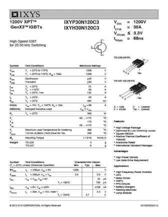
ixyp30n120c3 ixyh30n120c3.pdf
1200V XPTTM VCES = 1200V IXYP30N120C3 GenX3TM IGBTs IC110 = 30A IXYH30N120C3 VCE(sat) 3.3V tfi(typ) = 88ns High-Speed IGBT for 20-50 kHz Switching TO-220 (IXYP) Symbol Test Conditions Maximum Ratings VCES TJ = 25 C to 175 C 1200 V G C Tab E VCGR TJ = 25 C to 175 C, RGE = 1M 1200 V VGES Continuous 2
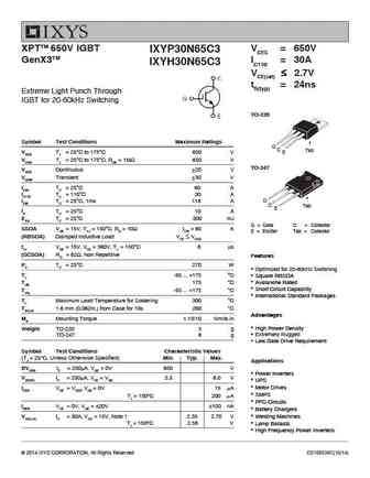
ixyp30n65c3.pdf
XPTTM 650V IGBT VCES = 650V IXYP30N65C3 GenX3TM IC110 = 30A IXYH30N65C3 VCE(sat) 2.7V tfi(typ) = 24ns Extreme Light Punch Through IGBT for 20-60kHz Switching TO-220 Symbol Test Conditions Maximum Ratings G C Tab VCES TJ = 25 C to 175 C 650 V E VCGR TJ = 25 C to 175 C, RGE = 1M 650 V TO-247 VGES Conti
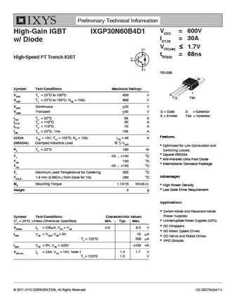
ixgp30n60b4d1.pdf
Preliminary Technical Information VCES = 600V High-Gain IGBT IXGP30N60B4D1 IC110 = 30A w/ Diode VCE(sat) 1.7V tfi(typ) = 88ns High-Speed PT Trench IGBT TO-220 Symbol Test Conditions Maximum Ratings G VCES TJ = 25 C to 150 C 600 V C Tab E VCGR TJ = 25 C to 150 C, RGE = 1M 600 V VGES Continuous 20 V VGEM Transient 30 V G = Gate C = Collector
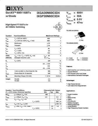
ixgp30n60c3.pdf
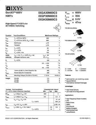
GenX3TM 600V VCES = 600V IXGA30N60C3 IGBTs IC110 = 30A IXGP30N60C3 VCE(sat) 3.0V IXGH30N60C3 tfi(typ) = 47ns High-Speed PT IGBTs for 40-100kHz Switching TO-263 AA (IXGA) G E Symbol Test Conditions Maximum Ratings C (Tab) VCES TC = 25 C to 150 C 600 V VCGR TJ = 25 C to 150 C, RGE = 1M 600 V TO-220AB (IXGP) VGES Continuous 20 V
ixgp30n120b3.pdf
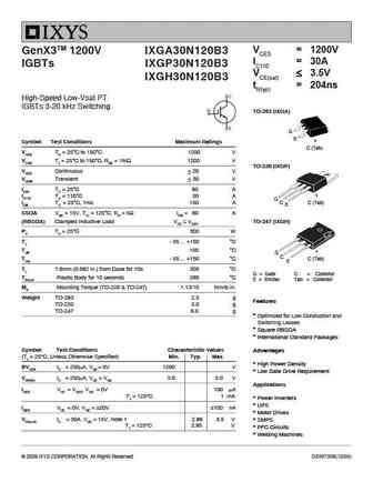
VCES = 1200V GenX3TM 1200V IXGA30N120B3 IC110 = 30A IGBTs IXGP30N120B3 VCE(sat) 3.5V IXGH30N120B3 tfi(typ) = 204ns High-Speed Low-Vsat PT IGBTs 3-20 kHz Switching TO-263 (IXGA) G E Symbol Test Conditions Maximum Ratings C (Tab) VCES TC = 25 C to 150 C 1200 V VCGR TJ = 25 C to 150 C, RGE = 1M 1200 V TO-220 (IXGP) VGES Continuous 20 V VGEM Tra
ixyp30n120c3.pdf
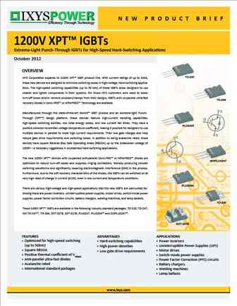
N E W P R O D U C T B R I E F Efficiency Through Technology 1200V XPT IGBTs Extreme-Light Punch-Through IGBTs for High-Speed Hard-Switching Applications October 2012 OVERVIEW TO-247 IXYS Corporation expands its 1200V XPT IGBT product line. With current ratings of up to 220A, these new devices are designed to minimize switching losses in high-voltage, hard-switching applica- tion
ixgp30n60b2.pdf
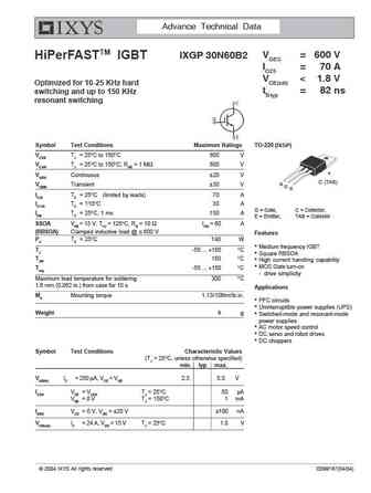
Advance Technical Data VCES = 600 V IXGP 30N60B2 HiPerFASTTM IGBT IC25 = 70 A VCE(sat)
ixgp30n60c3d4.pdf
GenX3TM 600V IGBTs VCES = 600V IXGA30N60C3D4 w/ Diode IC110 = 30A IXGP30N60C3D4 VCE(sat) 3.0V tfi(typ) = 47ns High-Speed PT IGBTs for 40-100kHz Switching TO-263 AA (IXGA) Symbol Test Conditions Maximum Ratings G E VCES TC = 25 C to 150 C 600 V C (Tab) VCGR TJ = 25 C to 150 C, RGE = 1M 600 V TO-220AB (IXGP) VGES Continuous 20 V
ixfa30n60x ixfp30n60x.pdf
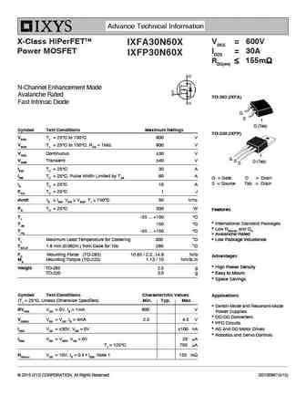
Advance Technical Information X-Class HiPerFETTM VDSS = 600V IXFA30N60X Power MOSFET ID25 = 30A IXFP30N60X RDS(on) 155m N-Channel Enhancement Mode Avalanche Rated TO-263 (IXFA) Fast Intrinsic Diode G S D (Tab) Symbol Test Conditions Maximum Ratings TO-220 (IXFP) VDSS TJ = 25 C to 150 C 600 V VDGR TJ = 25 C to 150 C, RGS = 1M
ixgp30n60c2.pdf
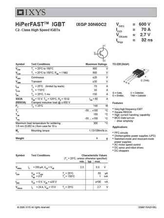
VCES = 600 V IXGP 30N60C2 HiPerFASTTM IGBT IC25 = 70 A C2- Class High Speed IGBTs VCE(sat) = 2.7 V tfi typ = 32 ns Symbol Test Conditions Maximum Ratings TO-220 (IXGP) VCES TJ = 25 C to 150 C 600 V VCGR TJ = 25 C to 150 C; RGE = 1 M 600 V VGES Continuous 20 V C (TAB) VGEM Transient 30 V G C E IC25 TC = 25 C (limited by leads) 70 A IC110 TC = 110 C30 A G = Gate, C =
ixgp30n60c3c1.pdf
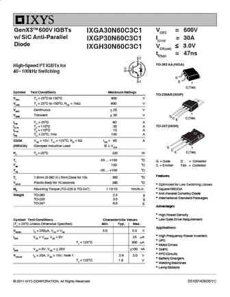
GenX3TM 600V IGBTs VCES = 600V IXGA30N60C3C1 w/ SiC Anti-Parallel IC110 = 30A IXGP30N60C3C1 Diode VCE(sat) 3.0V IXGH30N60C3C1 tfi(typ) = 47ns TO-263 AA (IXGA) High-Speed PT IGBTs for 40 - 100kHz Switching G E C (Tab) Symbol Test Conditions Maximum Ratings TO-220AB (IXGP) VCES TC = 25 C to 150 C 600 V VCGR TJ = 25 C to 150 C, RG
tip29-a-b-c tip30-a-b-c to-220.pdf
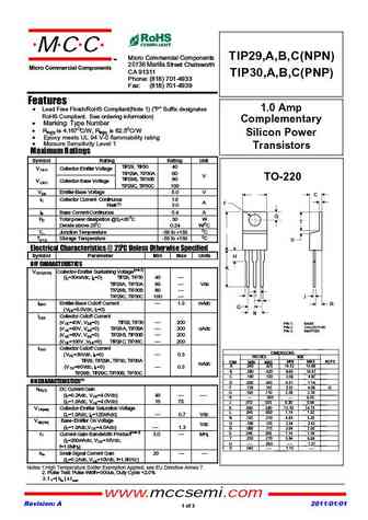
MCC Micro Commercial Components TM TIP29,A,B,C(NPN) 20736 Marilla Street Chatsworth Micro Commercial Components CA 91311 TIP30,A,B,C(PNP) Phone (818) 701-4933 Fax (818) 701-4939 Features Lead Free Finish/RoHS Compliant(Note 1) ("P" Suffix designates 1.0 Amp RoHS Compliant. See ordering information) Complementary Marking Type Number Rth(jc) is 4.167OC/W, Rth(ja) i
atp301.pdf

Ordering number ENA1457A ATP301 P-Channel Power MOSFET http //onsemi.com 100V, 28A, 75m , ATPAK Features ON-resistance RDS(on)=57m (typ.) Input capacitance Ciss=4000pF (typ.) 10V drive Halogen free compliance Specifications Absolute Maximum Ratings at Ta=25 C Parameter Symbol Conditions Ratings Unit Drain-to-Source Voltage VDSS --100 V Gate-t
tip29-a-b-c tip30-a-b-c.pdf
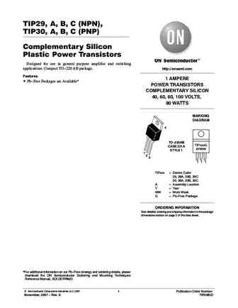
TIP29, A, B, C (NPN), TIP30, A, B, C (PNP) Complementary Silicon Plastic Power Transistors Designed for use in general purpose amplifier and switching applications. Compact TO-220 AB package. http //onsemi.com Features 1 AMPERE Pb-Free Packages are Available* POWER TRANSISTORS COMPLEMENTARY SILICON 40, 60, 80, 100 VOLTS, 80 WATTS MARKING DIAGRAM 4 TO-220AB TIPxxxG CASE 2
fgb3040g2-f085 fgd3040g2-f085 fgp3040g2-f085 fgi3040g2-f085.pdf

ON Semiconductor Is Now To learn more about onsemi , please visit our website at www.onsemi.com onsemi and and other names, marks, and brands are registered and/or common law trademarks of Semiconductor Components Industries, LLC dba onsemi or its affiliates and/or subsidiaries in the United States and/or other countries. onsemi owns the rights to a number of patents, trademarks,
atp302.pdf
Ordering number ENA1654A ATP302 P-Channel Power MOSFET http //onsemi.com 60V, 70A, 13m , ATPAK Features ON-resistance RDS(on)1=10m (typ.) Input capacitance Ciss=5400pF (typ.) 4.5V drive Halogen free compliance Specifications Absolute Maximum Ratings at Ta=25 C Parameter Symbol Conditions Ratings Unit Drain-to-Source Voltage VDSS --60 V Gate-t
tip29g tip29ag tip29bg tip29cg tip30g tip30ag tip30bg tip30cg.pdf
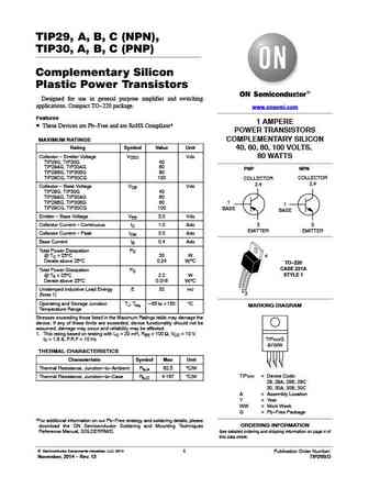
TIP29, A, B, C (NPN), TIP30, A, B, C (PNP) Complementary Silicon Plastic Power Transistors Designed for use in general purpose amplifier and switching applications. Compact TO-220 package. www.onsemi.com Features 1 AMPERE These Devices are Pb-Free and are RoHS Compliant* POWER TRANSISTORS MAXIMUM RATINGS COMPLEMENTARY SILICON Rating Symbol Value Unit 40, 60, 80, 100 VOLTS, Col
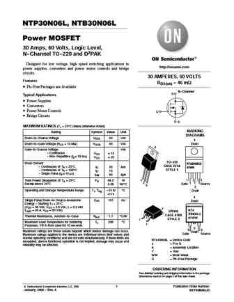
ntb30n06g ntp30n06 ntp30n06 ntb30n06.pdf
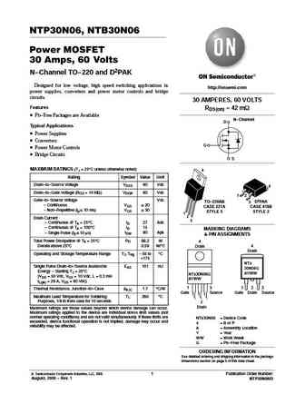
NTP30N06, NTB30N06 Power MOSFET 30 Amps, 60 Volts N-Channel TO-220 and D2PAK Designed for low voltage, high speed switching applications in http //onsemi.com power supplies, converters and power motor controls and bridge circuits. 30 AMPERES, 60 VOLTS Features RDS(on) = 42 mW Pb-Free Packages are Available N-Channel D Typical Applications Power Supplies Converters G
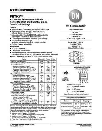
ntmsd3p303r2-d.pdf
NTMSD3P303R2 FETKY P-Channel Enhancement-Mode Power MOSFET and Schottky Diode Dual SO-8 Package Features High Efficiency Components in a Single SO-8 Package http //onsemi.com High Density Power MOSFET with Low RDS(on), MOSFET Schottky Diode with Low VF -3.05 AMPERES Independent Pin-Outs for MOSFET and Schottky Die -30 VOLTS Allowing for Flexibility in Application Use
atp304.pdf
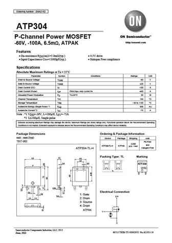
Ordering number ENA2192 ATP304 P-Channel Power MOSFET http //onsemi.com -60V, -100A, 6.5m , ATPAK Features On-resistance RDS(on)1=5.0m (typ.) 4.5V drive Input Capacitance Ciss=13000pF(typ.) Halogen Free compliance Specifications Absolute Maximum Ratings at Ta = 25 C Parameter Symbol Conditions Ratings Unit Drain to Source Voltage VDSS -60 V Gate to S
smp3003-dl-1e smp3003-tl-1e.pdf

Ordering number ENA1655D SMP3003 P-Channel Power MOSFET http //onsemi.com 75V, 100A, 8.0m , TO-263-2L/TO-263 Features TO-263 ON-resistance RDS(on)1=6.2m (typ.) 4V drive Input capacitance Ciss=13400pF (typ.) Specifications Absolute Maximum Ratings at Ta=25 C Parameter Symbol Conditions Ratings Unit Drain to Source Voltage VDSS --75 V Gate to Source
tip29 tip29a tip29b tip29c tip30 tip30a tip30b tip30c.pdf

TIP29, A, B, C (NPN), TIP30, A, B, C (PNP) Complementary Silicon Plastic Power Transistors Designed for use in general purpose amplifier and switching applications. Compact TO-220 package. www.onsemi.com Features 1 AMPERE These Devices are Pb-Free and are RoHS Compliant* POWER TRANSISTORS MAXIMUM RATINGS COMPLEMENTARY SILICON Rating Symbol Value Unit 40, 60, 80, 100 VOLTS, Col
tip3055 tip2955.pdf
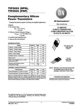
TIP3055 (NPN), TIP2955 (PNP) Complementary Silicon Power Transistors Designed for general-purpose switching and amplifier applications. http //onsemi.com Features DC Current Gain - 15 AMPERE hFE = 20 - 70 @ IC POWER TRANSISTORS = 4.0 Adc COMPLEMENTARY SILICON Collector-Emitter Saturation Voltage - 60 VOLTS, 90 WATTS VCE(sat) = 1.1 Vdc (Max) @ IC = 4.0 Adc Excell
ntp30n20 ntp30n20g.pdf
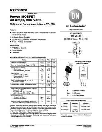
NTP30N20 Preferred Device Power MOSFET 30 Amps, 200 Volts N-Channel Enhancement-Mode TO-220 http //onsemi.com Features Source-to-Drain Diode Recovery Time Comparable to a Discrete 30 AMPERES Fast Recovery Diode 200 VOLTS Avalanche Energy Specified 68 mW @ VGS = 10 V (Typ) IDSS and RDS(on) Specified at Elevated Temperature Pb-Free Package is Available* N-Channel D
smp3003.pdf
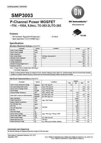
Ordering number ENA1655D SMP3003 P-Channel Power MOSFET http //onsemi.com 75V, 100A, 8.0m , TO-263-2L/TO-263 Features TO-263 ON-resistance RDS(on)1=6.2m (typ.) 4V drive Input capacitance Ciss=13400pF (typ.) Specifications Absolute Maximum Ratings at Ta=25 C Parameter Symbol Conditions Ratings Unit Drain to Source Voltage VDSS --75 V Gate to Source
mtp3055v.pdf
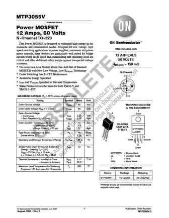
MTP3055V Preferred Device Power MOSFET 12 Amps, 60 Volts N-Channel TO-220 This Power MOSFET is designed to withstand high energy in the avalanche and commutation modes. Designed for low voltage, high http //onsemi.com speed switching applications in power supplies, converters and power motor controls, these devices are particularly well suited for bridge 12 AMPERES circuits where dio
mtp30p06v.pdf
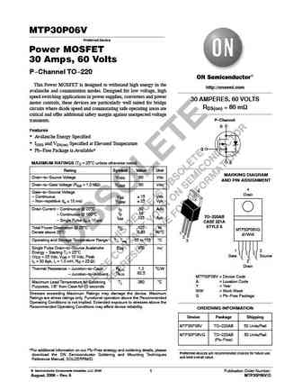
MTP30P06V Preferred Device Power MOSFET 30 Amps, 60 Volts P-Channel TO-220 This Power MOSFET is designed to withstand high energy in the http //onsemi.com avalanche and commutation modes. Designed for low voltage, high speed switching applications in power supplies, converters and power 30 AMPERES, 60 VOLTS motor controls, these devices are particularly well suited for bridge RDS(on)
tip3055.pdf
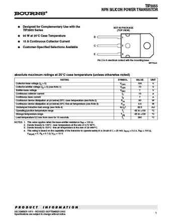
TIP3055 NPN SILICON POWER TRANSISTOR Designed for Complementary Use with the SOT-93 PACKAGE TIP2955 Series (TOP VIEW) 90 W at 25 C Case Temperature B 1 15 A Continuous Collector Current C 2 Customer-Specified Selections Available 3 E Pin 2 is in electrical contact with the mounting base. MDTRAAA absolute maximum ratings at 25 C case temperature (unless otherwis
fmp30n60s1.pdf
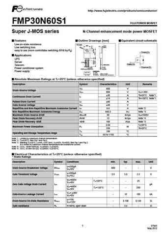
http //www.fujielectric.com/products/semiconductor/ FMP30N60S1 FUJI POWER MOSFET Super J-MOS series N-Channel enhancement mode power MOSFET Features Outline Drawings [mm] Equivalent circuit schematic Low on-state resistance TO-220 10+0.5 0 4.5 0.2 1.3 0.2 Low switching loss easy to use (more controllabe switching dV/dt by R ) g Drain(D) Applications UPS 1.2 0.2 Server PRE-
6mbp300vea060-50.pdf
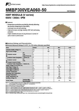
http //www.fujielectric.com/products/semiconductor/ 6MBP300VEA060-50 IGBT Modules IGBT MODULE (V series) 600V / 300A / IPM Features Temperature protection provided by directly detecting the junction temperature of the IGBTs Low power loss and soft switching High performance and high reliability IGBT with overheating protection Higher reliability because of a big decr
6mbp30rh060.pdf
IGBT Modules 6MBP30RH060 IGBT-IPM R series 600V / 30A / 6 in one-package Features Low power loss and soft switching High performance and high reliability IGBT with overheating protection Higher reliability because of a big decrease in number of parts in built-in control circuit Applications Inverter for motor drive AC and DC servo drive amplifier UPS (Uni
6mbp300ra060.pdf
6MBP300RA060 600V / 300A 6 in one-package IGBT-IPM R series Features Temperature protection provided by directly detecting the junction temperature of the IGBTs Low power loss and soft switching High performance and high reliability IGBT with overheating protection Higher reliability because of a big decrease in number of parts in built-in control circuit Maximum rati
7mbp300vea060-50.pdf
http //www.fujielectric.com/products/semiconductor/ 7MBP300VEA060-50 IGBT Modules IGBT MODULE (V series) 600V / 300A / IPM Features Temperature protection provided by directly detecting the junction temperature of the IGBTs Low power loss and soft switching High performance and high reliability IGBT with overheating protection Higher reliability because of a big decr
6mbp30vaa060-50.pdf
http //www.fujielectric.com/products/semiconductor/ 6MBP30VAA060-50 IGBT Modules IGBT MODULE (V series) 600V / 30A / IPM Features Temperature protection provided by directly detecting the junction temperature of the IGBTs Low power loss and soft switching Compatible with existing IPM-N series packages High performance and high reliability IGBT with overheating protec
gp300lss.pdf
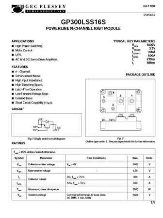
JULY 1996 GP300LSS16S ADVANCE ENGINEERING DATA DS4136-5.2 GP300LSS16S POWERLINE N-CHANNEL IGBT MODULE APPLICATIONS TYPICAL KEY PARAMETERS VCES 1600V High Power Switching. VCE(sat) 3.3V Motor Control. IC(CONT) 300A UPS. IC(PK) 600A AC And DC Servo Drive Amplifiers. tr 270ns tf 590ns FEATURES n - Channel. PACKAGE OUTLINE Enhancement Mode. High Input Impedance. High Sw
rfd3055-sm rfp3055.pdf
RFD3055, RFD3055SM S E M I C O N D U C T O R RFP3055 12A, 60V, Avalanche Rated, N-Channel Enhancement-Mode Power MOSFETs (MegaFETs) February 1994 Features Packaging JEDEC TO-220AB 12A, 60V TOP VIEW rDS(ON) = 0.150 SOURCE Temperature Compensating PSPICE Model DRAIN Peak Current vs Pulse Width Curve GATE UIS Rating Curve +175oC Operating Temperature JED
tip29 tip30 a b c.pdf
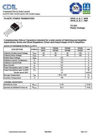
Continental Device India Limited An ISO/TS 16949, ISO 9001 and ISO 14001 Certified Company PLASTIC POWER TRANSISTORS TIP29, A, B, C NPN TIP30, A, B, C PNP TO-220 Plastic Package Complementary Silicon Transistors intended for a wide variety of Switching and Amplifier Applications, Series and Shunt Regulators, Driver and Output stages of Hi-Fi Amplifiers ABSOLUTE MAXIMUM RATINGS (Ta=25
tip2955f tip3055f.pdf
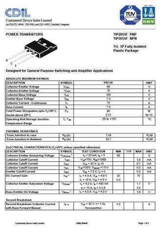
Continental Device India Limited An ISO/TS 16949, ISO 9001 and ISO 14001 Certified Company POWER TRANSISTORS TIP2955F PNP TIP3055F NPN TO- 3P Fully Isolated Plastic Package B C E Designed for General Purpose Switching and Amplifier Applications ABSOLUTE MAXIMUM RATINGS DESCRIPTION SYMBOL VALUE UNIT Collector-Emitter Voltage VCEO 60 V Collector-Emitter Voltage VCER 70 V Collector-
kmb7d6np30q.pdf
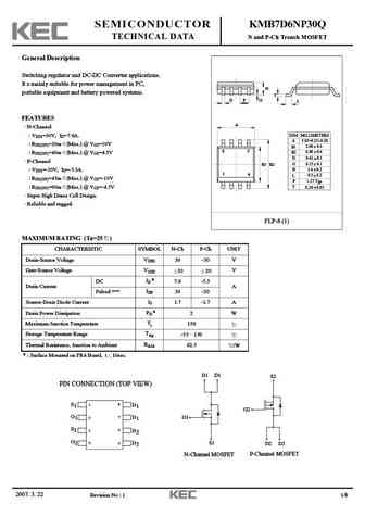
SEMICONDUCTOR KMB7D6NP30Q TECHNICAL DATA N and P-Ch Trench MOSFET General Description Switching regulator and DC-DC Converter applications. It s mainly suitable for power management in PC, H portable equipment and battery powered systems. T D P G L FEATURES A N-Channel DIM MILLIMETERS VDSS=30V, ID=7.6A. A 5.05+0.25/-0.20 RDS(ON)=20m (Max.) @ VGS=10V _ 3.90 + 0.3 B1 8 5
kmb5d5np30q.pdf
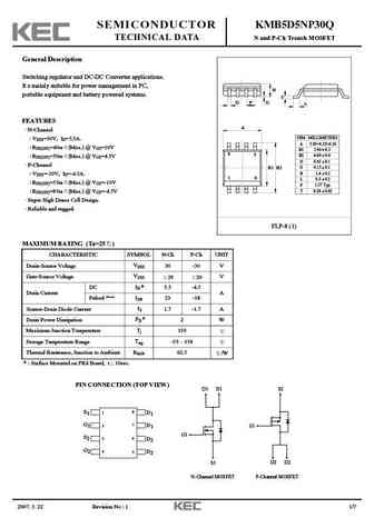
SEMICONDUCTOR KMB5D5NP30Q TECHNICAL DATA N and P-Ch Trench MOSFET General Description Switching regulator and DC-DC Converter applications. It s mainly suitable for power management in PC, H portable equipment and battery powered systems. T D P G L FEATURES A N-Channel DIM MILLIMETERS VDSS=30V, ID=5.5A. A 5.05+0.25/-0.20 RDS(ON)=40m (Max.) @ VGS=10V _ 3.90 + 0.3 B1 8 5
kmb010p30qa.pdf
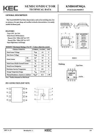
SEMICONDUCTOR KMB010P30QA TECHNICAL DATA P-Ch Trench MOSFET GENERAL DESCRIPTION This Trench MOSFET has better characteristics, such as fast switching time, low on resistance, low gate charge and excellent avalanche characteristiscs. It is mainly suitable for Battery pack. H T D P G L FEATURES A VDSS=-30V, ID=-10A. DIM MILLIMETERS A _ + Drain-Source ON Resistance. 4.85 0.2 B1 _
kmb3d0p30sa.pdf
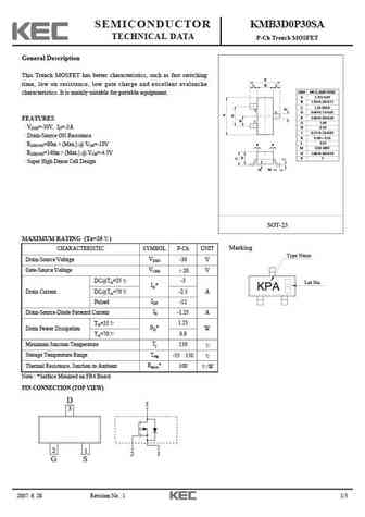
SEMICONDUCTOR KMB3D0P30SA TECHNICAL DATA P-Ch Trench MOSFET General Description This Trench MOSFET has better characteristics, such as fast switching E time, low on resistance, low gate charge and excellent avalanche L B L DIM MILLIMETERS characteristics. It is mainly suitable for portable equipment. _ + A 2.93 0.20 B 1.30+0.20/-0.15 C 1.30 MAX 2 3 D 0.40+0.15/-0.05 E 2.40+0.30
kma7d0np30q.pdf
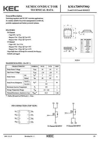
SEMICONDUCTOR KMA7D0NP30Q TECHNICAL DATA N and P-CH Trench MOSFET General Description Switching regulator and DC-DC converter applications. It s mainly suitable for power management in notebook, portable equipment and battery powered systems. A FEATURES 8 5 T N-Channel B1 B2 L VDSS=30V, ID=7A. 1 4 RDS(ON)=17m (Typ.) @ VGS=10V. RDS(ON)=22m (Typ.) @ VGS=4.5V. DIM MILLIMET
kmb8d0p30qa.pdf
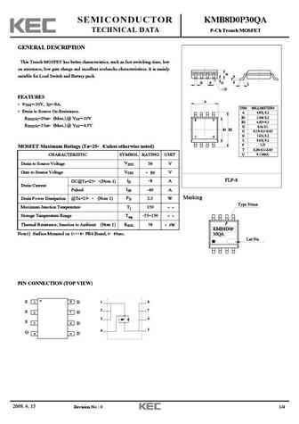
SEMICONDUCTOR KMB8D0P30QA TECHNICAL DATA P-Ch Trench MOSFET GENERAL DESCRIPTION This Trench MOSFET has better characteristics, such as fast switching time, low on resistance, low gate charge and excellent avalanche characteristiscs. It is mainly H suitable for Load Switch and Battery pack. T D P G L U FEATURES A VDSS=-30V, ID=-8A. DIM MILLIMETERS Drain to Source On Resistanc
kmb014p30qa.pdf
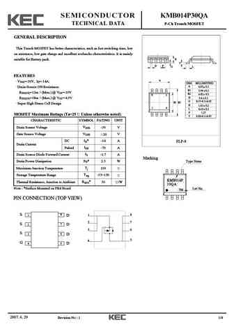
SEMICONDUCTOR KMB014P30QA TECHNICAL DATA P-Ch Trench MOSFET GENERAL DESCRIPTION This Trench MOSFET has better characteristics, such as fast switching time, low on resistance, low gate charge and excellent avalanche characteristiscs. It is mainly suitable for Battery pack. H T D P G L FEATURES A VDSS=-30V, ID=-14A. DIM MILLIMETERS A _ + Drain-Source ON Resistance. 4.85 0.2 B1 _
kmb7d1dp30qa.pdf
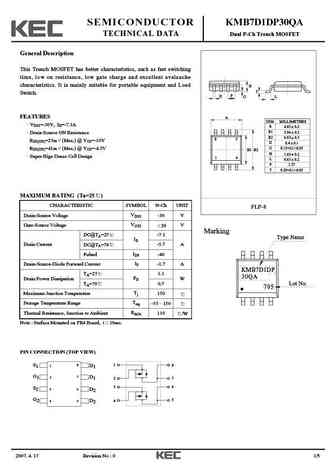
SEMICONDUCTOR KMB7D1DP30QA TECHNICAL DATA Dual P-Ch Trench MOSFET General Description This Trench MOSFET has better characteristics, such as fast switching time, low on resistance, low gate charge and excellent avalanche characteristics. It is mainly suitable for portable equipment and Load H T Switch. D P G L FEATURES A DIM MILLIMETERS VDSS=-30V, ID=-7.1A A _ 4.85 0.2 + B1 _
kmd4d5p30xa.pdf
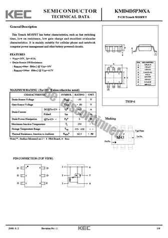
SEMICONDUCTOR KMD4D5P30XA TECHNICAL DATA P-CH Trench MOSFET General Description This Trench MOSFET has better characteristics, such as fast switching time, low on resistance, low gate charge and excellent avalanche characteristics. It is mainly suitable for cellular phone and netebook computer power management and other battery powered circuits. D H J FEATURES E VDSS=-30V, ID=-4.
kmb7d0np30qa.pdf
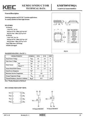
SEMICONDUCTOR KMB7D0NP30QA TECHNICAL DATA N and P-Ch Trench MOSFET General Description Switching regulator and DC-DC Converter applications. It s mainly suitable for Back-light Inverter. H T D P G L FEATURES N-Channel A VDSS=30V, ID=7A. DIM MILLIMETERS A _ + RDS(ON)=23.5m (Max.) @ VGS=10V 4.85 0.2 B1 _ 3.94 + 0.2 RDS(ON)=39m (Max.) @ VGS=4.5V B2 _ 6.02+ 0.3 8 5 D _
kmb7d0np30q.pdf
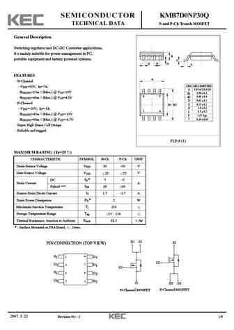
SEMICONDUCTOR KMB7D0NP30Q TECHNICAL DATA N and P-Ch Trench MOSFET General Description Switching regulator and DC-DC Converter applications. It s mainly suitable for power management in PC, H portable equipment and battery powered systems. T D P G L FEATURES A N-Channel DIM MILLIMETERS VDSS=30V, ID=7A. A 5.05+0.25/-0.20 RDS(ON)=25m (Max.) @ VGS=10V _ 3.90 + 0.3 B1 8 5 _
kmb8d0p30q.pdf
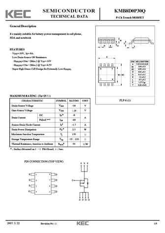
SEMICONDUCTOR KMB8D0P30Q TECHNICAL DATA P-Ch Trench MOSFET General Description It s mainly suitable for battery power management in cell phone, PDA and notebook H T D P G L FEATURES VDSS=-30V, ID=-8A. A Low Drain-Source ON Resistance. RDS(ON)=20m (Max.) @ VGS=-10V DIM MILLIMETERS A 5.05+0.25/-0.20 RDS(ON)=35m (Max.) @ VGS=-4.5V _ 3.90 + 0.3 B1 8 Super High Dense Cell
fkp300a.pdf
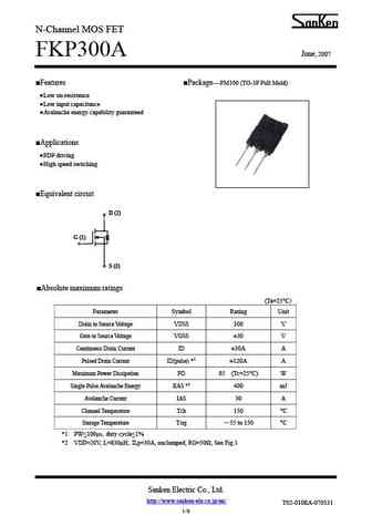
N-Channel MOS FET FKP300A June, 2007 Features Package---FM100 (TO-3P Full Mold) Low on-resistance Low input capacitance Avalanche energy capability guaranteed Applications PDP driving High speed switching Equivalent circuit D (2) G (1) S (3) Absolute maximum ratings (Ta=25 C Parameter Symbol Rating Unit Drain to Source Voltage V
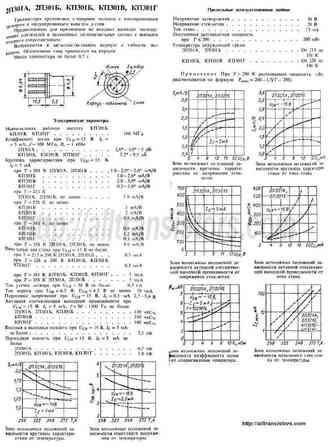
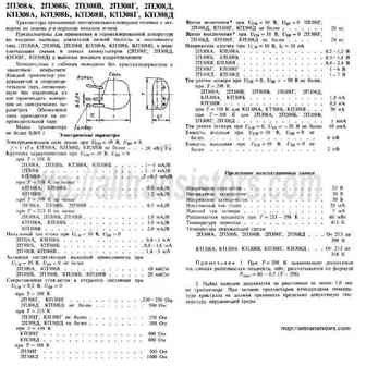
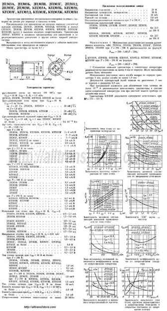
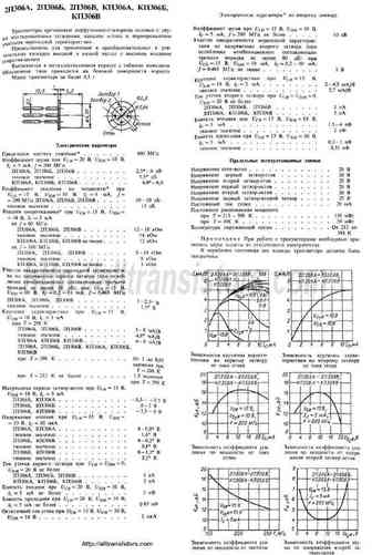
2p302a.pdf

p-n n-. 2302 P max, 300 U max,B 20 U max,B 20 U max,B 10 I max, 24 Tmax, C 125 U ,B 1...3.5 I,A 10 U,B 10 S,/ 5...12 U, 7 I , 3...24 11, 20 12, 8
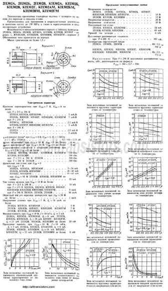
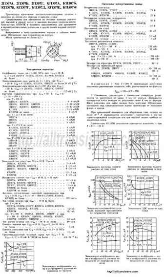
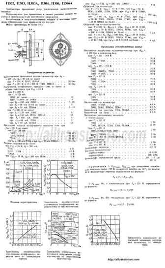
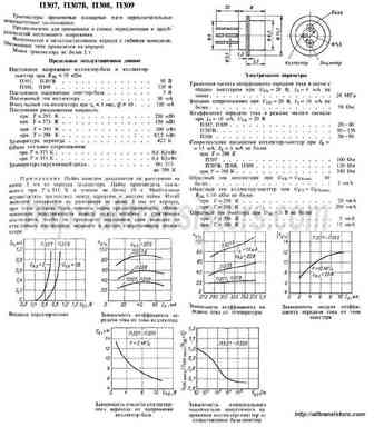
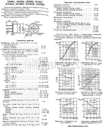
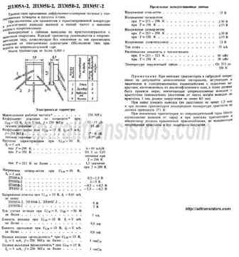
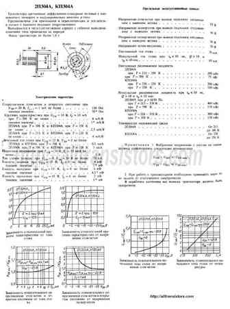
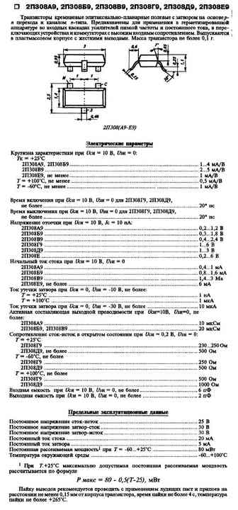
cep3060 ceb3060.pdf
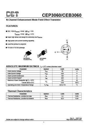
CEP3060/CEB3060 N-Channel Enhancement Mode Field Effect Transistor FEATURES 30V, 105A,RDS(ON) = 6m @VGS = 10V. RDS(ON) = 8m @VGS = 4.5V. Super high dense cell design for extremely low RDS(ON). D High power and current handing capability. Lead free product is acquired. TO-220 & TO-263 package. G CEB SERIES CEP SERIES S TO-263(DD-PAK) TO-220 ABSOLUTE MAXIMUM RATINGS Tc = 25
cep30n15l ceb30n15l.pdf
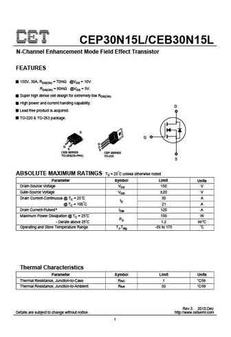
CEP30N15L/CEB30N15L N-Channel Enhancement Mode Field Effect Transistor FEATURES 150V, 30A, RDS(ON) = 70m @VGS = 10V. RDS(ON) = 80m @VGS = 5V. Super high dense cell design for extremely low RDS(ON). High power and current handing capability. D Lead free product is acquired. TO-220 & TO-263 package. G CEB SERIES CEP SERIES TO-263(DD-PAK) TO-220 S ABSOLUTE MAXIMUM RATINGS T
ceb30n3 cef30n3 cep30n3.pdf
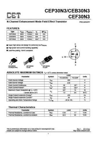
CEP30N3/CEB30N3 CEF30N3 N-Channel Enhancement Mode Field Effect Transistor PRELIMINARY FEATURES Type VDSS RDS(ON) ID @VGS CEP30N3 300V 110m 30A 10V CEB30N3 300V 110m 30A 10V CEF30N3 300V 110m 30A e 10V D Super high dense cell design for extremely low RDS(ON). High power and current handing capability. Lead-free plating ; RoHS compliant. G S CEB SERIES CEP SERIES CEF SERI
cep30p03 ceb30p03.pdf
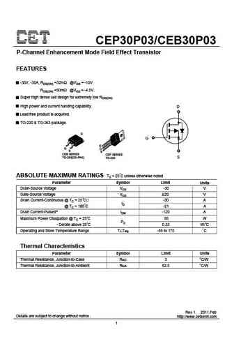
CEP30P03/CEB30P03 P-Channel Enhancement Mode Field Effect Transistor FEATURES -30V, -30A, RDS(ON) =32m @VGS = -10V. RDS(ON) =50m @VGS = -4.5V. Super high dense cell design for extremely low RDS(ON). High power and current handing capability. D Lead free product is acquired. TO-220 & TO-263 package. G CEB SERIES CEP SERIES TO-263(DD-PAK) S TO-220 ABSOLUTE MAXIMUM RATINGS Tc
ap30t10gs-hf.pdf
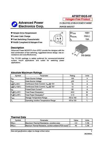
AP30T10GS-HF Halogen-Free Product Advanced Power N-CHANNEL ENHANCEMENT MODE Electronics Corp. POWER MOSFET Simple Drive Requirement D BVDSS 100V Lower Gate Charge RDS(ON) 55m Fast Switching Characteristic ID 19A G RoHS Compliant & Halogen-Free S Description Advanced Power MOSFETs from APEC provide the designer with the best combination of fast switching, ruggedized
ap30g100w.pdf
AP30G100W RoHS-compliant Product Advanced Power N-CHANNEL INSULATED GATE Electronics Corp. BIPOLAR TRANSISTOR Features VCES 1000V High speed switching IC 30A Low Saturation Voltage VCE(sat)=3.0V@IC=30A C G Industry Standard TO-3P Package G C RoHS Compliant TO-3P E E Absolute Maximum Ratings Symbol Parameter Rating Units VCES Collector-Emitter Voltage 1000 V VG
ap30p10gs.pdf
AP30P10GS RoHS-compliant Product Advanced Power P-CHANNEL ENHANCEMENT MODE Electronics Corp. POWER MOSFET Lower Gate Charge D BVDSS -100V Simple Drive Requirement RDS(ON) 80m Fast Switching Characteristic ID -25A G S Description Advanced Power MOSFETs from APEC provide the designer with the best combination of fast switching, ruggedized device design, low on-resistance
ap30t10gm.pdf
AP30T10GM-HF Halogen-Free Product Advanced Power N-CHANNEL ENHANCEMENT MODE Electronics Corp. POWER MOSFET Simple Drive Requirement BVDSS 100V D D D Lower Gate Charge RDS(ON) 55m D Fast Switching Characteristic ID3 4.5A G S S Halogen Free & RoHS Compliant S SO-8 D Description AP30T10 series are from Advanced Power innovated design and silicon process techno
ap30t10gk-hf.pdf
AP30T10GK-HF Halogen-Free Product Advanced Power N-CHANNEL ENHANCEMENT MODE Electronics Corp. POWER MOSFET Simple Drive Requirement D BVDSS 100V Lower Gate Charge RDS(ON) 55m Fast Switching Characteristic ID 4.8A G Halogen Free & RoHS Compliant Product S Description D Advanced Power MOSFETs from APEC provide the designer with the best combination of fast switching
ap30t10gi-hf.pdf
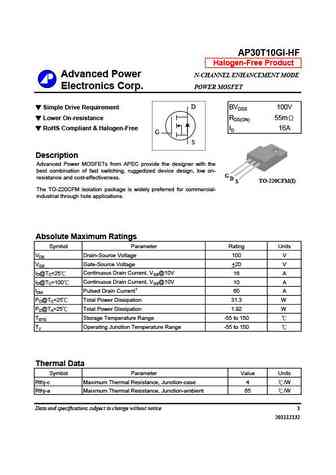
AP30T10GI-HF Halogen-Free Product Advanced Power N-CHANNEL ENHANCEMENT MODE Electronics Corp. POWER MOSFET Simple Drive Requirement D BVDSS 100V Lower On-resistance RDS(ON) 55m RoHS Compliant & Halogen-Free ID 16A G S Description Advanced Power MOSFETs from APEC provide the designer with the best combination of fast switching, ruggedized device design, low on- G resis
ap30t10gh.pdf
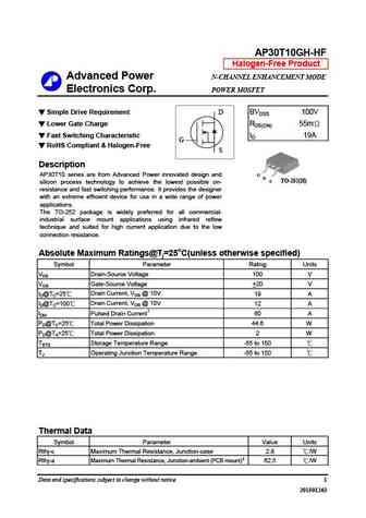
AP30T10GH-HF Halogen-Free Product Advanced Power N-CHANNEL ENHANCEMENT MODE Electronics Corp. POWER MOSFET Simple Drive Requirement D BVDSS 100V Lower Gate Charge RDS(ON) 55m Fast Switching Characteristic ID 19A G RoHS Compliant & Halogen-Free S Description AP30T10 series are from Advanced Power innovated design and G D S TO-252(H) silicon process technology to
ap30t10gi.pdf
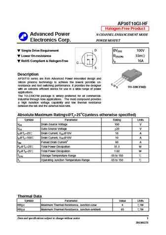
AP30T10GI-HF Halogen-Free Product Advanced Power N-CHANNEL ENHANCEMENT MODE Electronics Corp. POWER MOSFET Simple Drive Requirement D BVDSS 100V Lower On-resistance RDS(ON) 55m RoHS Compliant & Halogen-Free ID 16A G S Description AP30T10 series are from Advanced Power innovated design and silicon process technology to achie
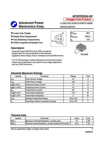
ap30g120sw.pdf
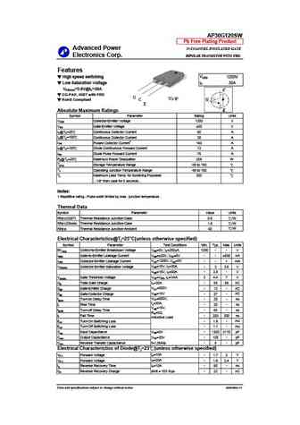
AP30G120SW Pb Free Plating Product Advanced Power N-CHANNEL INSULATED GATE Electronics Corp. BIPOLAR TRANSISTOR WITH FRD. Features High speed switching VCES 1200V Low Saturation Voltage IC 30A VCE(sat)=3.0V@IC=30A C CO-PAK, IGBT with FRD G TO-3P G RoHS Compliant C E E Absolute Maximum Ratings Symbol Parameter Rating Units VCES Collector-Emitter Voltage 1200 V
ap30p10gs-hf.pdf
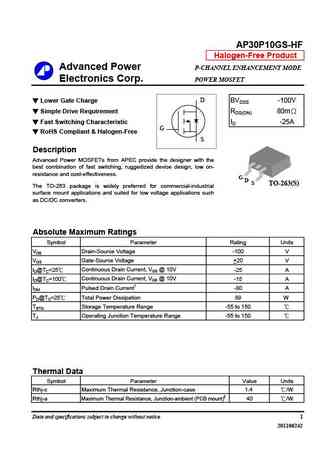
AP30P10GS-HF Halogen-Free Product Advanced Power P-CHANNEL ENHANCEMENT MODE Electronics Corp. POWER MOSFET Lower Gate Charge D BVDSS -100V Simple Drive Requirement RDS(ON) 80m Fast Switching Characteristic ID -25A G RoHS Compliant & Halogen-Free S Description Advanced Power MOSFETs from APEC provide the designer with the best combination of fast switching, ruggediz
ap30n30w.pdf
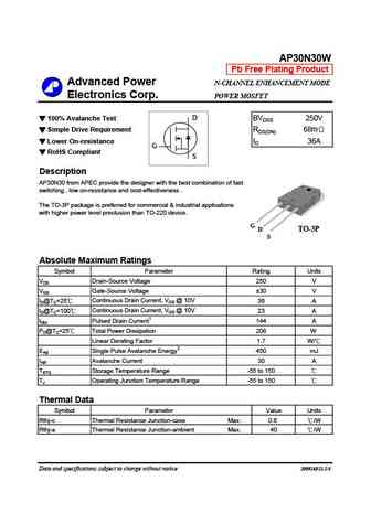
AP30N30W Pb Free Plating Product Advanced Power N-CHANNEL ENHANCEMENT MODE Electronics Corp. POWER MOSFET D 100% Avalanche Test BVDSS 250V Simple Drive Requirement RDS(ON) 68m Lower On-resistance ID 36A G RoHS Compliant S Description AP30N30 from APEC provide the designer with the best combination of fas
ap30t10gs.pdf
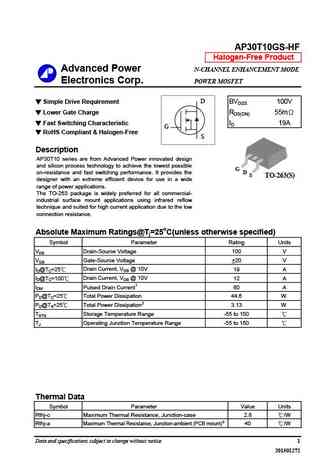
AP30T10GS-HF Halogen-Free Product Advanced Power N-CHANNEL ENHANCEMENT MODE Electronics Corp. POWER MOSFET Simple Drive Requirement D BVDSS 100V Lower Gate Charge RDS(ON) 55m Fast Switching Characteristic ID 19A G RoHS Compliant & Halogen-Free S Description AP30T10 series are from Advanced Power innovated design and silicon process technology to achieve the lowest
ap30t10gp-hf.pdf
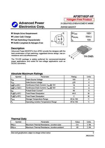
AP30T10GP-HF Halogen-Free Product Advanced Power N-CHANNEL ENHANCEMENT MODE Electronics Corp. POWER MOSFET Simple Drive Requirement D BVDSS 100V Lower Gate Charge RDS(ON) 55m Fast Switching Characteristic ID 19A G RoHS Compliant & Halogen-Free S Description Advanced Power MOSFETs from APEC provide the designer with the best combination of fast switching, ruggedized
ap30p10gi.pdf
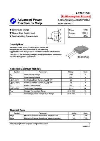
AP30P10GI RoHS-compliant Product Advanced Power P-CHANNEL ENHANCEMENT MODE Electronics Corp. POWER MOSFET Lower Gate Charge D BVDSS -100V Simple Drive Requirement RDS(ON) 80m Fast Switching Characteristic ID -25A G S Description Advanced Power MOSFETs from APEC provide the designer with the best combination of fast switching, ruggedized device design, low on-resistance
ap30t10gk.pdf
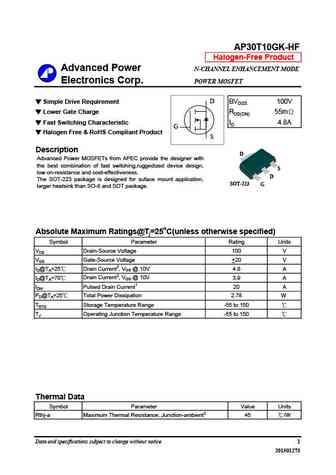
AP30T10GK-HF Halogen-Free Product Advanced Power N-CHANNEL ENHANCEMENT MODE Electronics Corp. POWER MOSFET Simple Drive Requirement D BVDSS 100V Lower Gate Charge RDS(ON) 55m Fast Switching Characteristic ID 4.8A G Halogen Free & RoHS Compliant Product S Description D Advanced Power MOSFETs from APEC provide the designer with the best combination of fast switching
ap30p10gh.pdf
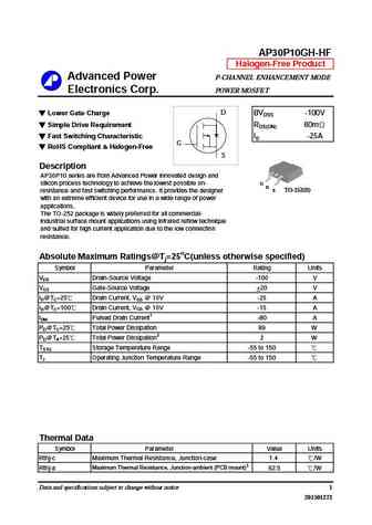
AP30P10GH-HF Halogen-Free Product Advanced Power P-CHANNEL ENHANCEMENT MODE Electronics Corp. POWER MOSFET Lower Gate Charge D BVDSS -100V Simple Drive Requirement RDS(ON) 80m Fast Switching Characteristic ID -25A G RoHS Compliant & Halogen-Free S Description AP30P10 series are from Advanced Power innovat
ap30p10gp.pdf
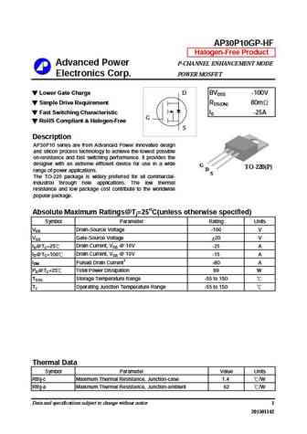
AP30P10GP-HF Halogen-Free Product Advanced Power P-CHANNEL ENHANCEMENT MODE Electronics Corp. POWER MOSFET Lower Gate Charge D BVDSS -100V Simple Drive Requirement RDS(ON) 80m Fast Switching Characteristic ID -25A G RoHS Compliant & Halogen-Free S Description AP30P10 series are from Advanced Power innovat
ap30g120bsw-hf.pdf
AP30G120BSW-HF Halogen-Free Product Advanced Power N-CHANNEL INSULATED GATE Electronics Corp. BIPOLAR TRANSISTOR WITH FRD. Features High Speed Switching VCES 1200V Low Saturation Voltage IC 30A VCE(sat)=2.9V@IC=30A C CO-PAK, IGBT With FRD G C TO-3P G RoHS Compliant & Halogen-Free E E Absolute Maximum Ratings Symbol Parameter Rating Units VCES Collector-Emitter
ap30g120w.pdf
AP30G120W Pb Free Plating Product Advanced Power N-CHANNEL INSULATED GATE Electronics Corp. BIPOLAR TRANSISTOR Features VCES 1100V High speed switching IC 30A Low Saturation Voltage VCE(sat)=3.0V@IC=30A C G Industry Standard TO-3P Package G RoHS Compliant TO-3P C E E Absolute Maximum Ratings Symbol Parameter Rating Units VCES Collector-Emitter Voltage 1100 V
ap30p10gh-hf.pdf
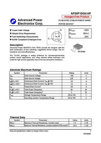
AP30P10GH-HF Halogen-Free Product Advanced Power P-CHANNEL ENHANCEMENT MODE Electronics Corp. POWER MOSFET Lower Gate Charge D BVDSS -100V Simple Drive Requirement RDS(ON) 80m Fast Switching Characteristic ID -25A G RoHS Compliant & Halogen-Free S Description Advanced Power MOSFETs from APEC provide the designer with the best combination of fast switching, ruggediz
ap30g120asw.pdf
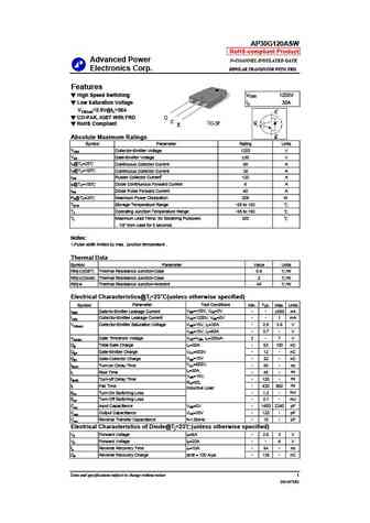
AP30G120ASW RoHS-compliant Product Advanced Power N-CHANNEL INSULATED GATE Electronics Corp. BIPOLAR TRANSISTOR WITH FRD. Features High Speed Switching VCES 1200V Low Saturation Voltage IC 30A VCE(sat)=2.9V@IC=30A C CO-PAK, IGBT With FRD G C TO-3P G RoHS Compliant E E Absolute Maximum Ratings Symbol Parameter Rating Units VCES Collector-Emitter Voltage 1200 V
ap30g120csw-hf.pdf

AP30G120CSW-HF Halogen-Free Product Advanced Power N-CHANNEL INSULATED GATE Electronics Corp. BIPOLAR TRANSISTOR WITH FRD. Features High Speed Switching VCES 1200V Low Saturation Voltage IC 30A VCE(sat)=2.9V@IC=30A C CO-PAK, IGBT With FRD G C TO-3P G RoHS Compliant & Halogen-Free E E Absolute Maximum Ratings Symbol Parameter Rating Units VCES Collector-Emitter
ap30g40geo-hf.pdf
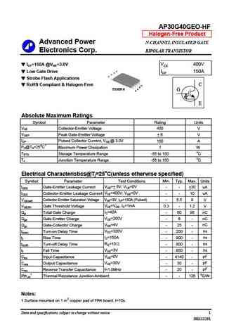
AP30G40GEO-HF Halogen-Free Product Advanced Power N-CHANNEL INSULATED GATE Electronics Corp. BIPOLAR TRANSISTOR ICP=150A @VGE=3.0V VCE 400V C Low Gate Drive ICP 150A C C C Strobe Flash Applications RoHS Compliant & Halogen-Free C G E E TSSOP-8 G E E Absolute Maximum Ratings Symbol Parameter Rating Units VCE Collector-Emitter Voltage 400 V VGEP Peak Gate-E
ap30t10gh-hf.pdf
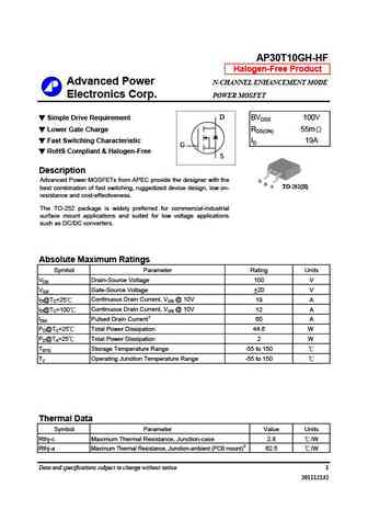
AP30T10GH-HF Halogen-Free Product Advanced Power N-CHANNEL ENHANCEMENT MODE Electronics Corp. POWER MOSFET Simple Drive Requirement D BVDSS 100V Lower Gate Charge RDS(ON) 55m Fast Switching Characteristic ID 19A G RoHS Compliant & Halogen-Free S Description Advanced Power MOSFETs from APEC provide the designer with the G D S TO-252(H) best combination of fast sw
ap30n30wi.pdf
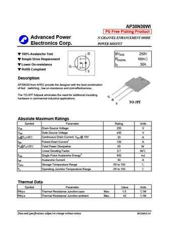
AP30N30WI Pb Free Plating Product Advanced Power N-CHANNEL ENHANCEMENT MODE Electronics Corp. POWER MOSFET D 100% Avalanche Test BVDSS 250V Simple Drive Requirement RDS(ON) 68m Lower On-resistance ID 30A G RoHS Compliant S Description AP30N30 from APEC provide the designer with the best combination of f
ap30p10gp-hf.pdf
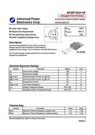
AP30P10GP-HF Halogen-Free Product Advanced Power P-CHANNEL ENHANCEMENT MODE Electronics Corp. POWER MOSFET Lower Gate Charge D BVDSS -100V Simple Drive Requirement RDS(ON) 80m Fast Switching Characteristic ID -25A G RoHS Compliant & Halogen-Free S Description Advanced Power MOSFETs from APEC provide the designer with the best combination of fast switching, ruggedi
ap30t10gm-hf.pdf
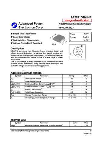
AP30T10GM-HF Halogen-Free Product Advanced Power N-CHANNEL ENHANCEMENT MODE Electronics Corp. POWER MOSFET Simple Drive Requirement BVDSS 100V D D D Lower Gate Charge RDS(ON) 55m D Fast Switching Characteristic ID 4.5A G S S Halogen Free & RoHS Compliant S SO-8 D Description AP30T10 series are from Advanced Power innovated design and silicon process technol
afp3050s.pdf
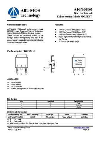
AFP3050S Alfa-MOS 30V P-Channel Technology Enhancement Mode MOSFET General Description Features AFP3050S, P-Channel enhancement mode -30V/-9A,RDS(ON)=60m @VGS=-10V MOSFET, uses Advanced Trench Technology -30V/-7A,RDS(ON)=72m @VGS=-4.5V to provide excellent RDS(ON), low gate charge. -30V/-5A,RDS(ON)=108m @VGS=-2.5V These devices are particularly suited for low
mtp3001n3.pdf
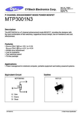
Spec. No. C400N3 Issued Date 2006.10.17 CYStech Electronics Corp. Revised Date Page No. 1/5 P-CHANNEL ENHANCEMENT MODE POWER MOSFET MTP3001N3 Description The MTP3001N3 is a P-channel enhancement-mode MOSFET, providing the designer with the best combination of fast switching, ruggedized device design, low on-resistance and cost effectiveness. Features @V =-10V,
p3010bv.pdf
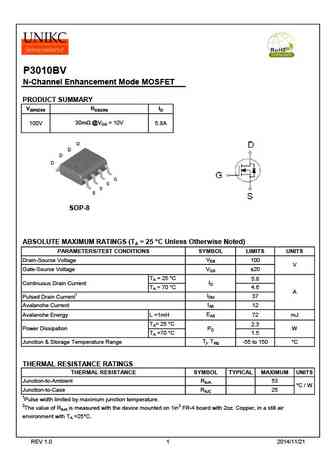
P3010BV N-Channel Enhancement Mode MOSFET PRODUCT SUMMARY V(BR)DSS RDS(ON) ID 30m @VGS = 10V 100V 5.8A SOP-8 ABSOLUTE MAXIMUM RATINGS (TA = 25 C Unless Otherwise Noted) PARAMETERS/TEST CONDITIONS SYMBOL LIMITS UNITS Drain-Source Voltage VDS 100 V VGS Gate-Source Voltage 20 TA = 25 C 5.8 ID Continuous Drain Current TA = 70 C 4.6 A IDM 37 Pulsed Drain Current
p3004bd.pdf
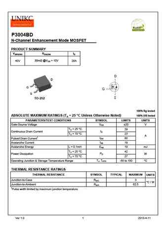
P3004BD N-Channel Enhancement Mode MOSFET PRODUCT SUMMARY V(BR)DSS RDS(ON) ID 30m @VGS = 10V 40V 29A TO-252 100% Rg tested 100% UIS tested ABSOLUTE MAXIMUM RATINGS (TA = 25 C Unless Otherwise Noted) PARAMETERS/TEST CONDITIONS SYMBOL LIMITS UNITS VGS Gate-Source Voltage 20 V TC = 25 C 29 ID Continuous Drain Current TC = 70 C 23 A IDM 80 Pulsed Drain Current1
p3003edg.pdf
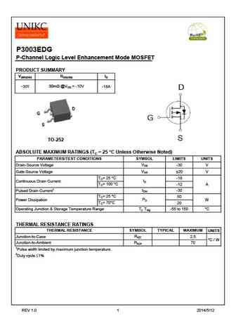
P3003EDG P-Channel Logic Level Enhancement Mode MOSFET PRODUCT SUMMARY V(BR)DSS RDS(ON) ID 30m @VGS = -10V -18A -30V TO-252 ABSOLUTE MAXIMUM RATINGS (TC = 25 C Unless Otherwise Noted) PARAMETERS/TEST CONDITIONS SYMBOL LIMITS UNITS VDS Drain-Source Voltage -30 V VGS Gate-Source Voltage 20 V TC= 25 C -18 ID Continuous Drain Current TC= 100 C -12 A IDM -30 Pul
p3055ldg.pdf
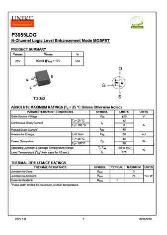
P3055LDG N-Channel Logic Level Enhancement Mode MOSFET PRODUCT SUMMARY V(BR)DSS RDS(ON) ID 90m @VGS = 10V 25V 12A TO-252 ABSOLUTE MAXIMUM RATINGS (TC = 25 C Unless Otherwise Noted) PARAMETERS/TEST CONDITIONS SYMBOL LIMITS UNITS VGS Gate-Source Voltage 20 V TC= 25 C 12 ID Continuous Drain Current TC= 100 C 8 A IDM 45 Pulsed Drain Current1 EAS Avalanche Energy
p3055llg.pdf
P3055LLG N-Channel Enhancement Mode MOSFET PRODUCT SUMMARY V(BR)DSS RDS(ON) ID 25V 72m @VGS = 10V 6A SOT- 223 ABSOLUTE MAXIMUM RATINGS (TA = 25 C Unless Otherwise Noted) PARAMETERS/TEST CONDITIONS SYMBOL LIMITS UNITS Gate-Source Voltage VGS 20 V TA = 25 C 6 ID Continuous Drain Current TA = 70 C 3.3 A IDM 21 Pulsed Drain Current2 IAS Avalanche Current 12 Av
hfp30n06.pdf
HFP30N06 Shantou Huashan Electronic Devices Co.,Ltd. N-Channel Enhancement Mode Field Effect Transistor General Description TO-220 This Power MOSFET is produced using advanced planar stripe, DMOS technology. This latest technology has been especially designed to minimize on-state resistance, have a low gate charge with superior switching performance, and rugged avalanche ch
dh100p30.pdf
DH100P30/DH100P30F/DH100P30I/ DH100P30E/DH100P30B/DH100P30D 30A 100V P-channel Enhancement Mode Power MOSFET 1 Description These P-channel Enhanced VDMOSFETs, Used V -100V DSS = advanced trench technology and design, provide to excellent R with low gate charge. Which accords R DSON DS(on) TYP) =35m with the RoHS standard. I = -30A D 2 Features Fast Switching Low ON
dmp3030sn.pdf
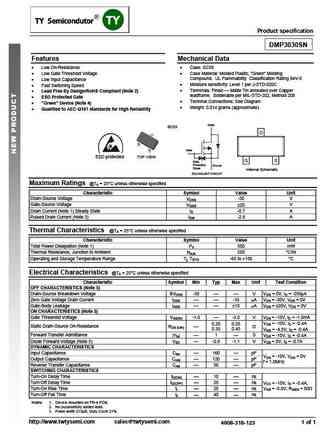
Product specification DMP3030SN Features Mechanical Data Low On-Resistance Case SC59 Low Gate Threshold Voltage Case Material Molded Plastic, Green Molding Compound. UL Flammability Classification Rating 94V-0 Low Input Capacitance Moisture sensitivity Level 1 per J-STD-020C Fast Switching Speed Terminals Finish Matte Tin annealed ove
dmp3098l.pdf
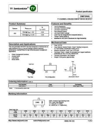
Product specification DMP3098L P-CHANNEL ENHANCEMENT MODE MOSFET Product Summary Features and Benefits Low On-Resistance ID Low Gate Threshold Voltage V(BR)DSS RDS(on) max TA = 25 C Low Input Capacitance Fast Switching Speed 70m @ VGS = -10V -3.8A Low Input/Output Leakage -30V 120m @ VGS =-4.5V -3.0A Lead Free By Design/RoHS Compliant (Note 1)
ftk55p30d.pdf
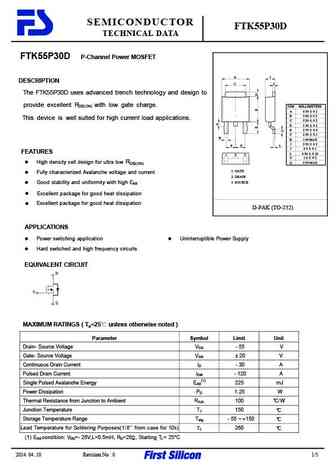
SEMICONDUCTOR FTK55P30D TECHNICAL DATA FTK55P30D P-Channel Power MOSFET A I DESCRIPTION C J The FTK55P30D uses advanced trench technology and design to provide excellent RDS(ON) with low gate charge. DIM MILLIMETERS A 6 50 0 2 B 5 60 0 2 This device is well suited for high current load applications. C 5 20 0 2 D 1 50 0 2 E 2 70 0 2 F 2 30 0 1 H H 1 00
mxp3007ct-cd.pdf
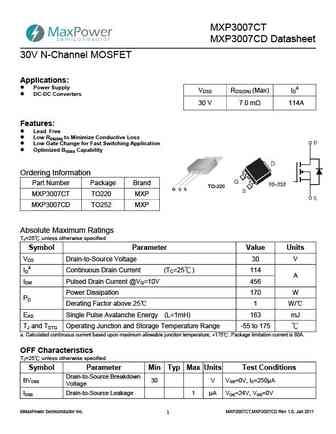
MXP3007CT MXP3007CD Datasheet 30V N-Channel MOSFET Applications Power Supply VDSS RDS(ON) (Max) IDa DC-DC Converters 30 V 7.0 m 114A Features Lead Free Low RDS(ON) to Minimize Conductive Loss Low Gate Change for Fast Switching Application Optimized BVDSS Capability Ordering Information Part Number Package Brand MXP3007CT TO220 MXP MXP
dh100p30a dh100p30af dh100p30ai dh100p30ae dh100p30ab dh100p30ad.pdf
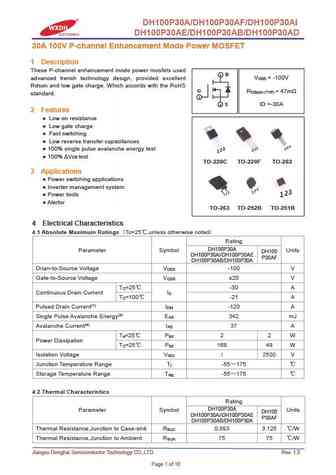
DH100P30A/DH100P30AF/DH100P30AI DH100P30AE/DH100P30AB/DH100P30AD 30A 100V P-channel Enhancement Mode Power MOSFET 1 Description These P-channel enhancement mode power mosfets used 2 D advanced trench technology design, provided excellent V = -100V DSS Rdson and low gate charge. Which accords with the RoHS G R = 47m DS(on) (TYP) standard. 1 3 S ID =-30A 2 Features Low on r
dh100p30d.pdf
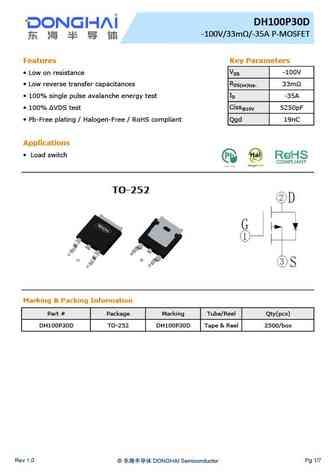
DH100P30D -100V/33m /-35A P-MOSFET Features Key Parameters VDS Low on resistance -100V RDS(on)typ. Low reverse transfer capacitances 33m ID 100% single pulse avalanche energy test -35A Ciss@10V 100% VDS test 5250pF Pb-Free plating / Halogen-Free / RoHS compliant Qgd 19nC Applications Load switch TO-252 Marking & Packing Information Part # Package
dh100p30c dh100p30cf dh100p30ci dh100p30ce dh100p30cb dh100p30cd.pdf
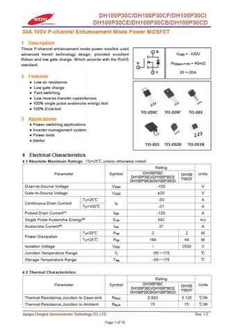
DH100P30C/DH100P30CF/DH100P30CI DH100P30CE/DH100P30CB/DH100P30CD 30A 100V P-channel Enhancement Mode Power MOSFET 1 Description These P-channel enhancement mode power mosfets used 2 D advanced trench technology design, provided excellent V = -100V DSS Rdson and low gate charge. Which accords with the RoHS G R = 40m DS(on) (TYP) standard. 1 3 S ID =-30A 2 Features Low on r
sgtp30v60fd2pu.pdf
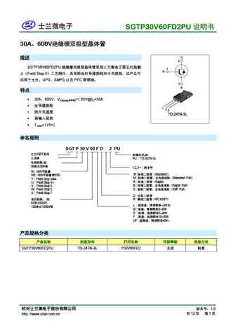
SGTP30V60FD2PU 30A 600V C 2 SGTP30V60FD2PU 1 G Field Stop 5 UPS SMPS PFC 3 E 30A 600V VCE(sat)( )=1.65V@IC=30A
blvp304.pdf
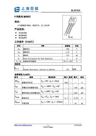
BLVP304 P MOSFET P MOSFET P MOSFET P MOSFET P VDMOS (T=25 ) (T=25 ) (T=25 )
ncep3085eg.pdf
Pb Free Product http //www.ncepower.com NCEP3085EG NCE N-Channel Super Trench Power MOSFET Description The NCEP3085EG uses Super Trench technology that is uniquely optimized to provide the most efficient high frequency switching performance. Both conduction and switching power losses are minimized due to an extremely low combination of RDS(ON) and Qg. This device is ideal for hi
nce01p30k.pdf
http //www.ncepower.com NCE01P30K NCE P-Channel Enhancement Mode Power MOSFET Description The NCE01P30K uses advanced trench technology and design to provide excellent R with low gate charge. It can DS(ON) be used in a wide variety of applications. It is ESD protested. General Features V =-100V,I =-30A Schematic diagram DS D R
ncep30p90k.pdf
http //www.ncepower.com NCEP30P90K NCE P-Channel Super Trench Power MOSFET Description The NCEP30P90K uses Super Trench technology that is uniquely optimized to provide the most efficient high frequency switching performance. Both conduction and switching power losses are minimized due to an extremely low combination of R and Q . This device is ideal for DS(ON) g high-frequency switchi
ncep3065qu.pdf
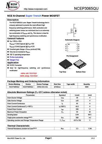
http //www.ncepower.com NCEP3065QU NCE N-Channel Super Trench Power MOSFET Description The NCEP3065QU uses Super Trench technology that is uniquely optimized to provide the most efficient high frequency switching performance. Both conduction and switching power losses are minimized due to an extremely low combination of R and Q . This device is ideal for DS(ON) g high-frequency switchi
ncep30t17gu.pdf
Pb Free Product http //www.ncepower.com NCEP30T17GU NCE N-Channel Super Trench Power MOSFET Description The NCEP30T17GU uses Super Trench technology that is uniquely optimized to provide the most efficient high frequency switching performance. Both conduction and switching power losses are minimized due to an extremely low combination of R and Q . This device is ideal for DS(ON) g hig
ncep30t17g.pdf

Pb Free Product http //www.ncepower.com NCEP30T17G NCE N-Channel Super Trench Power MOSFET Description The NCEP30T17G uses Super Trench technology that is uniquely optimized to provide the most efficient high frequency switching performance. Both conduction and switching power losses are minimized due to an extremely low combination of RDS(ON) and Qg. This device is ideal for
ncep3060eq.pdf
Pb Free Product http //www.ncepower.com NCEP3060EQ NCE N-Channel Super Trench Power MOSFET Description The NCEP3060EQ uses Super Trench technology that is uniquely optimized to provide the most efficient high frequency switching performance. Both conduction and switching power losses are minimized due to an extremely low combination of RDS(ON) and Qg. This device is ideal for hi
ncea15p30k.pdf
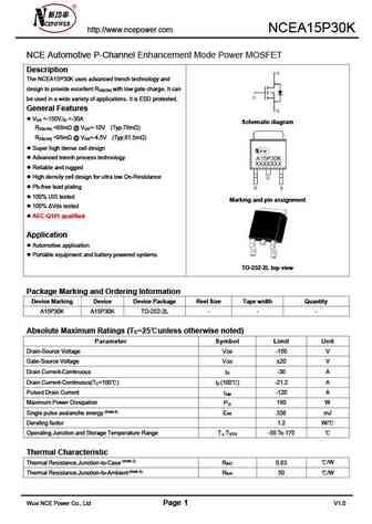
http //www.ncepower.com NCEA15P30K NCE Automotive P-Channel Enhancement Mode Power MOSFET Description The NCEA15P30K uses advanced trench technology and design to provide excellent R with low gate charge. It can DS(ON) be used in a wide variety of applications. It is ESD protested. General Features V =-150V,I =-30A DS D Schematic diagram R
ncep3090gu.pdf

Pb Free Product http //www.ncepower.com NCEP3090GU NCE N-Channel Super Trench Power MOSFET Description The NCEP3090GU uses Super Trench technology that is uniquely optimized to provide the most efficient high frequency switching performance. Both conduction and switching power losses are minimized due to an extremely low combination of RDS(ON) and Qg. This device is ideal for hi
ncep30t21gu.pdf
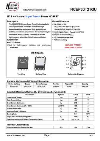
http //www.ncepower.com NCEP30T21GU NCE N-Channel Super Trench Power MOSFET Description General Features The NCEP30T21GU uses Super Trench technology that is V =30V,I =210A DS D uniquely optimized to provide the most efficient high R =0.72m (typical) @ V =10V DS(ON) GS frequency switching performance. Both conduction and R =0.85m (typical) @ V =4.5V DS(ON) GS switching power lo
ncep3045bgu.pdf
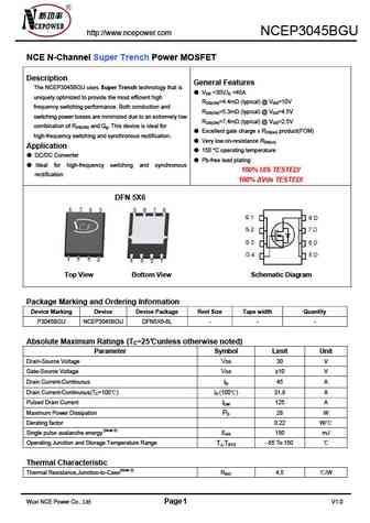
http //www.ncepower.com NCEP3045BGU NCE N-Channel Super Trench Power MOSFET Description General Features The NCEP3045BGU uses Super Trench technology that is VDS =30V,ID =45A uniquely optimized to provide the most efficient high RDS(ON)=4.4m (typical) @ VGS=10V frequency switching performance. Both conduction and RDS(ON)=5.3m (typical) @ VGS=4.5V switching power los
ncep30pt16g.pdf
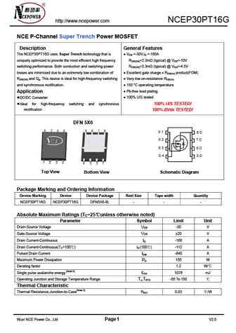
http //www.ncepower.com NCEP30PT16G NCE P-Channel Super Trench Power MOSFET Description General Features The NCEP30PT16G uses Super Trench technology that is VDS =-30V,ID =-160A uniquely optimized to provide the most efficient high frequency RDS(ON)=2.3m (typical) @ VGS=-10V switching performance. Both conduction and switching power RDS(ON)=3.3m (typical) @ VGS=-4.5V losse
ncep30t22gu.pdf

http //www.ncepower.com NCEP30T22GU NCE N-Channel Super Trench Power MOSFET Description General Features The NCEP30T22GU uses Super Trench technology that is V =30V,I =220A DS D uniquely optimized to provide the most efficient high R =0.62m (typical) @ V =10V DS(ON) GS frequency switching performance. Both conduction and R =0.80m (typical) @ V =4.5V DS(ON) GS switching power lo
ncep30t19g.pdf

Pb Free Product http //www.ncepower.com NCEP30T19G NCE N-Channel Super Trench Power MOSFET Description The NCEP30T19G uses Super Trench technology that is uniquely optimized to provide the most efficient high frequency switching performance. Both conduction and switching power losses are minimized due to an extremely low combination of RDS(ON) and Qg. This device is ideal for
ncep30t12g.pdf

Pb Free Product http //www.ncepower.com NCEP30T12G NCE N-Channel Super Trench Power MOSFET Description The NCEP30T12G uses Super Trench technology that is uniquely optimized to provide the most efficient high frequency switching performance. Both conduction and switching power losses are minimized due to an extremely low combination of RDS(ON) and Qg. This device is ideal for
nce55p30.pdf
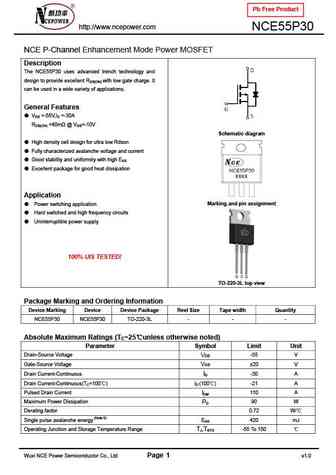
Pb Free Product http //www.ncepower.com NCE55P30 NCE P-Channel Enhancement Mode Power MOSFET Description The NCE55P30 uses advanced trench technology and design to provide excellent RDS(ON) with low gate charge. It can be used in a wide variety of applications. General Features VDS =-55V,ID =-30A RDS(ON)
ncep30p90g.pdf
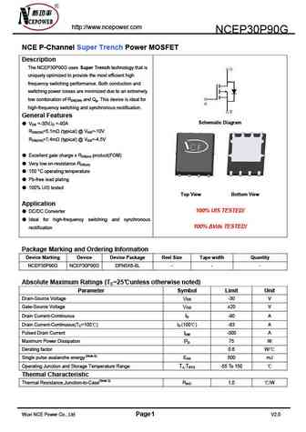
http //www.ncepower.com NCEP30P90G NCE P-Channel Super Trench Power MOSFET Description The NCEP30P90G uses Super Trench technology that is uniquely optimized to provide the most efficient high frequency switching performance. Both conduction and switching power losses are minimized due to an extremely low combination of RDS(ON) and Qg. This device is ideal for high-frequency sw
ncep15p30a.pdf
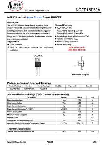
http //www.ncepower.com NCEP15P30A NCE P-Channel Super Trench Power MOSFET Description The NCEP15P30A uses Super Trench technology that is General Features uniquely optimized to provide the most efficient high frequency V =-150V,I =-30A DS D switching performance. Both conduction and switching power R =83m (typical) @ V =-10V DS(ON) GS losses are minimized due to an extremely lo
ncep3065bqu.pdf
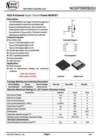
http //www.ncepower.com NCEP3065BQU NCE N-Channel Super Trench Power MOSFET Description The NCEP3065BQU uses Super Trench technology that is uniquely optimized to provide the most efficient high frequency switching performance. Both conduction and switching power losses are minimized due to an extremely low combination of R and Q . This device is ideal for DS(ON) g high-frequency switc
nce15p30.pdf
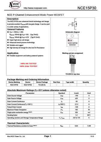
http //www.ncepower.com NCE15P30 NCE P-Channel Enhancement Mode Power MOSFET Description The NCE15P30 uses advanced trench technology and design to provide excellent R with low gate charge. It can be used DS(ON) in a wide variety of applications. General Features V =-150V,I =-30A Schematic diagram DS D R
ncep3045gu.pdf
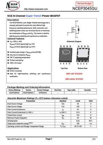
Pb Free Product http //www.ncepower.com NCEP3045GU NCE N-Channel Super Trench Power MOSFET Description The NCEP3045GU uses Super Trench technology that is uniquely optimized to provide the most efficient high frequency switching performance. Both conduction and switching power losses are minimized due to an extremely low combination of RDS(ON) and Qg. This device is ideal for hi
ncep30t15gu.pdf
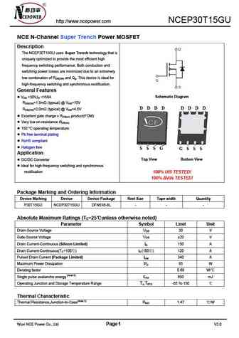
http //www.ncepower.com NCEP30T15GU NCE N-Channel Super Trench Power MOSFET Description The NCEP30T15GU uses Super Trench technology that is uniquely optimized to provide the most efficient high frequency switching performance. Both conduction and switching power losses are minimized due to an extremely low combination of RDS(ON) and Qg. This device is ideal for high-frequency sw
nceap30t17gu.pdf
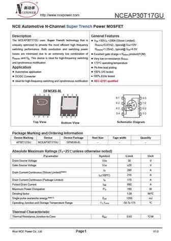
http //www.ncepower.com NCEAP30T17GU NCE Automotive N-Channel Super Trench Power MOSFET Description General Features The NCEAP30T17GU uses Super Trench technology that is V =30V,I =290A (Silicon Limited) DS D uniquely optimized to provide the most efficient high frequency R =0.97m , typical@ V =10V DS(ON) GS switching performance. Both conduction and switching power R =1.25m ,
ncep15p30ak.pdf

http //www.ncepower.com NCEP15P30AK NCE P-Channel Super Trench Power MOSFET Description The NCEP15P30AK uses Super Trench technology that is General Features uniquely optimized to provide the most efficient high frequency V =-150V,I =-29.5A DS D switching performance. Both conduction and switching power R =90m (typical) @ V =-10V DS(ON) GS losses are minimized due to an extremel
nce01p30i.pdf
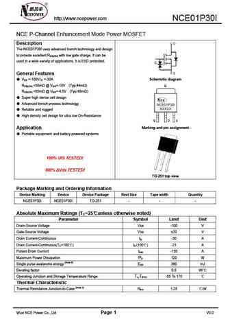
http //www.ncepower.com NCE01P30I NCE P-Channel Enhancement Mode Power MOSFET Description The NCE01P30I uses advanced trench technology and design to provide excellent RDS(ON) with low gate charge. It can be used in a wide variety of applications. It is ESD protested. General Features VDS =-100V,ID =-30A Schematic diagram RDS(ON)
nce30p30k.pdf
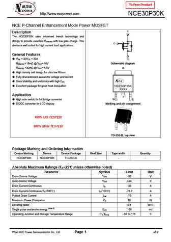
Pb Free Product http //www.ncepower.com NCE30P30K NCE P-Channel Enhancement Mode Power MOSFET Description The NCE30P30K uses advanced trench technology and design to provide excellent RDS(ON) with low gate charge .This device is well suited for high current load applications. General Features VDS =-30V,ID =-30A RDS(ON)
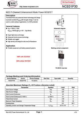
nce01p30l.pdf
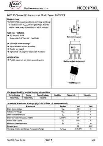
http //www.ncepower.com NCE01P30L NCE P-Channel Enhancement Mode Power MOSFET Description The NCE01P30L uses advanced trench technology and design to provide excellent RDS(ON) with low gate charge. It can be used in a wide variety of applications. It is ESD protested. General Features VDS =-100V,ID =-30A Schematic diagram RDS(ON)
ncep30t13gu.pdf
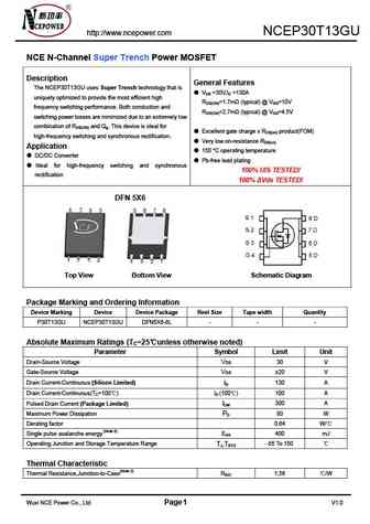
http //www.ncepower.com NCEP30T13GU NCE N-Channel Super Trench Power MOSFET Description General Features The NCEP30T13GU uses Super Trench technology that is VDS =30V,ID =130A uniquely optimized to provide the most efficient high RDS(ON)=1.7m (typical) @ VGS=10V frequency switching performance. Both conduction and RDS(ON)=2.7m (typical) @ VGS=4.5V switching power loss
nce30p30g.pdf
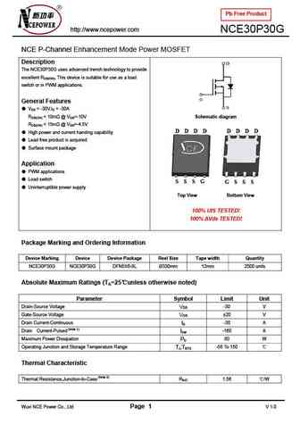
Pb Free Product http //www.ncepower.com NCE30P30G NCE P-Channel Enhancement Mode Power MOSFET Description The NCE30P30G uses advanced trench technology to provide excellent RDS(ON), This device is suitable for use as a load switch or in PWM applications. General Features VDS = -30V,ID = -30A RDS(ON)
ncep40p30k.pdf
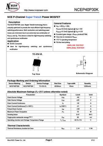
http //www.ncepower.com NCEP40P30K NCE P-Channel Super Trench Power MOSFET Description General Features The NCEP40P30K uses Super Trench technology that is V =-40V,I =-30A DS D uniquely optimized to provide the most efficient high frequency R =22.5m (typical) @ V =-10V DS(ON) GS switching performance. Both conduction and switching power R =31.5m (typical) @ V =-4.5V DS(ON) G
ncep40p30q.pdf
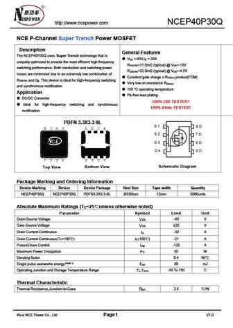
http //www.ncepower.com NCEP40P30Q NCE P-Channel Super Trench Power MOSFET Description General Features The NCEP40P30Q uses Super Trench technology that is V =-40V,I =-30A DS D uniquely optimized to provide the most efficient high frequency R =21.0m (typical) @ V =-10V DS(ON) GS switching performance. Both conduction and switching power R =32.0m (typical) @ V =-4.5V DS(ON) G
ncep3040q.pdf
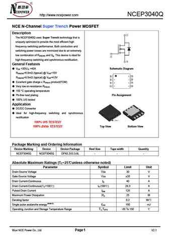
http //www.ncepower.com NCEP3040Q NCE N-Channel Super Trench Power MOSFET Description The NCEP3040Q uses Super Trench technology that is uniquely optimized to provide the most efficient high frequency switching performance. Both conduction and switching power losses are minimized due to an extremely low combination of RDS(ON) and Qg. This device is ideal for high-frequency switch
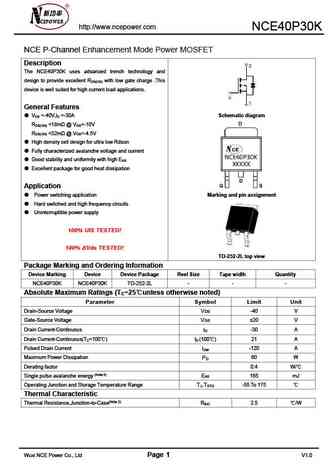
nce01p30d.pdf
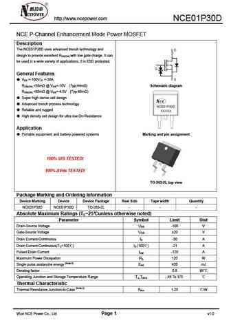
http //www.ncepower.com NCE01P30D NCE P-Channel Enhancement Mode Power MOSFET Description The NCE01P30D uses advanced trench technology and design to provide excellent RDS(ON) with low gate charge. It can be used in a wide variety of applications. It is ESD protested. General Features VDS =-100V,ID =-30A RDS(ON)
nce15p30k.pdf
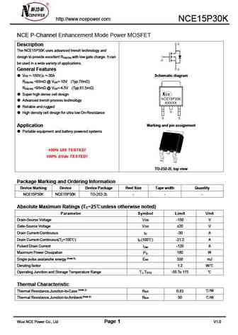
http //www.ncepower.com NCE15P30K NCE P-Channel Enhancement Mode Power MOSFET Description The NCE15P30K uses advanced trench technology and design to provide excellent R with low gate charge. It can DS(ON) be used in a wide variety of applications. General Features V =-150V,I =-30A Schematic diagram DS D R
nce55p30k.pdf
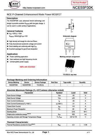
Pb Free Product http //www.ncepower.com NCE55P30K NCE P-Channel Enhancement Mode Power MOSFET Description The NCE55P30K uses advanced trench technology and design to provide excellent RDS(ON) with low gate charge. It can be used in a wide variety of applications. General Features VDS =-55V,ID =-30A RDS(ON)
p3010bv.pdf
P3010BV N-Channel Enhancement Mode NIKO-SEM SOP-8 Field Effect Transistor Halogen-Free & Lead-Free D PRODUCT SUMMARY V(BR)DSS RDS(ON) ID G 100V 30m 5.8A G GATE D DRAIN S SOURCE S ABSOLUTE MAXIMUM RATINGS (TA = 25 C Unless Otherwise Noted) PARAMETERS/TEST CONDITIONS SYMBOL LIMITS UNITS Drain-Source Voltage VDS 100 V Gate-Source Voltage VGS 20 V TA = 2
pnmdp30v60.pdf

PNMDP30V60 N-Channel MOSFET Description The MOSFET provide the best combination of fast switching, low on-resistance and cost-effectiveness. MOSFET Product Summary D (2) VDS(V) RDS(on)(m ) ID(A) 30 8.3@VGS=10V 60 G (1) S (3) Absolute maximum rating@25 Parameter Symbol Maximum Units Drain-Source Voltage VDS 30 V Gate-Source Voltage VGS 20 V TA=25 60 Drai
pnm8p30v20.pdf
PNM8P30V20 N-Channel 30-V(D-S) MOSFET Description The MOSFET provide the best combination of fast switching, low on-resistance and cost-effectiveness. MOSFET Product Summary VDS(V) RDS(on)(m ) ID(A) 30 3.7@ VGS=4.5V 23 Internal Structure Top View (SOP-8) D S D 1 8 S 2 7 D 6 G 3 D S 5 4 D G S Absolute maximum rating@25 Parameter Symbol Maximum
ppm8p30v10.pdf
PPM8P30V10 P-Channel MOSFET Description The enhancement mode MOS is extremely high density cell and low on-resistance. D 5 6 7 8 MOSFET Product Summary VDS(V) RDS(on)( ) ID(A) G 4 0.011 @ VGS=-10V -30 -11 0.015@ VGS=-4.5V S 2 1 3 Electrical characteristics per line@25 ( unless otherwise specified) Parameter Symbol Conditions Min. Typ.
pnm8p30v12.pdf
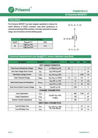
PNM8P30V12 N-Channel MOSFET Description The N-channel MOSFET has been designed specifically to improve the D 5 6 7 8 overall efficiency of DC/DC converters using either synchronous or conventional switching PWM controllers. It has been optimized for low gate charge, low on-resistance and fast switching speed. G 4 MOSFET Product Summary VDS(V) RDS(on)(m ) I
pnmdp30v90.pdf
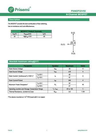
PNMDP30V90 N-Channel MOSFET Description The MOSFET provide the best combination of fast switching, low on-resistance and cost-effectiveness. MOSFET Product Summary D (2) VDS(V) RDS(on)(m ) ID(A) 30 4@VGS=10V 80 G (1) S (3) Absolute maximum rating@25 Parameter Symbol Maximum Units Drain-Source Voltage VDS 30 V Gate-Source Voltage VGS 20 V TA=25 80 Drain
ps06p30sa.pdf
PS06P30SA 30V Single Channel PMOSEFT Revision 1.0 Update Date Apr. 2011 ProsPower Microelectronics Co., Ltd PS06P30SA 30V Single Channel PMOSFET 2. Applications 1. General Description PWM applications The PS06P30SA uses advanced trench technology Load switch and design to provide excellent Rds(on) with low Power management gate charge and operation with gate vol
ps04p30sa.pdf
PS04P30SA 30V Single Channel PMOSEFT Revision 1.0 Update Date Apr. 2011 ProsPower Microelectronics Co., Ltd PS04P30SA 30V Single Channel PMOSFET 2. Applications 1. General Description PWM applications The PS04P30SA uses advanced trench technology Load switch and design to provide excellent Rds(on) with low Power management gate charge and operation with gate vol
ps06p30da.pdf
PS06P30DA 30V Dual Channel PMOSEFT Revision 1.0 Update Date Apr. 2011 ProsPower Microelectronics Co., Ltd PS06P30DA 30V Dual Channel PMOSFET 2. Applications 1. General Description PWM applications The PS06P30DA uses advanced trench technology Load switch and design to provide excellent Rds(on) with low Power management gate charge and operation with gate voltage
ps04p30sb.pdf
PS04P30SB 30V Single Channel PMOSEFT Revision 1.0 Update Date Apr. 2011 ProsPower Microelectronics Co., Ltd PS04P30SB 30V Single Channel PMOSFET 2. Applications 1. General Description PWM applications The PS04P30SB uses advanced trench technology Load switch and design to provide excellent Rds(on) with low Power management gate charge and operation with gate vol
hrp30n04k.pdf
December 2014 BVDSS = 40 V RDS(on) typ = 2.5m HRP30N04K ID = 230 A 40V N-Channel Trench MOSFET TO-220 FEATURES Originative New Design Superior Avalanche Rugged Technology 1 2 3 Excellent Switching Characteristics 1.Gate 2. Drain 3. Source Unrivalled Gate Charge 200 nC (Typ.) Extended Safe Operating Area Lower RDS(ON) 2.5 m (Typ.
stp3052d.pdf
STP3052D P Channel Enhancement Mode MOSFET -25.0A DESCRIPTION STP3052D is the P-Channel logic enhancement mode power field effect transistor which is produced using high cell density, DMOS trench technology. This high density process is especially tailored to minimize on-state resistance. These devices are particularly suited for low voltage application. Such as DC/DC converter
wm02p30me.pdf
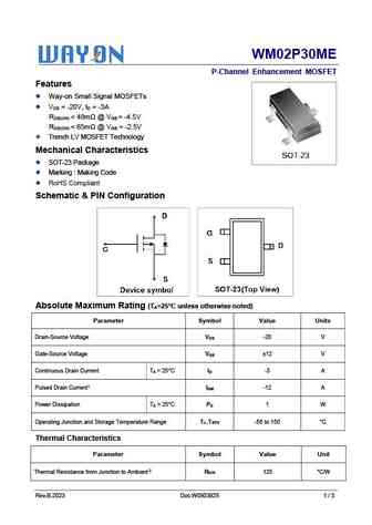
WM02P30ME P-Channel Enhancement MOSFET Features Way-on Small Signal MOSFETs V = -20V, I = -3A DS D R
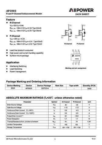
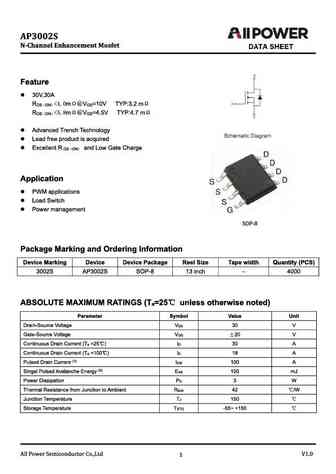
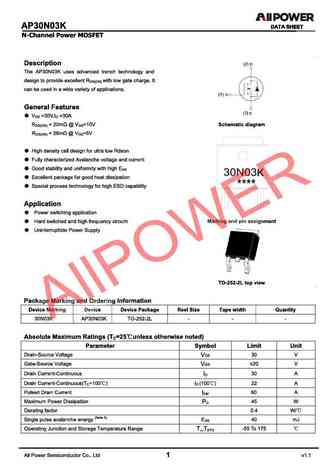
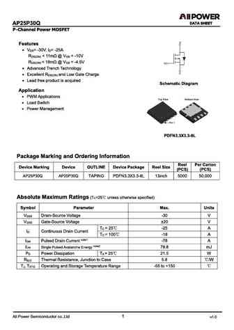
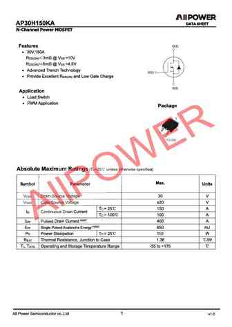
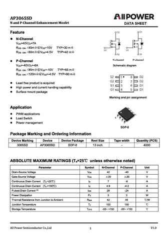
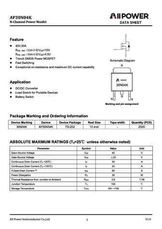
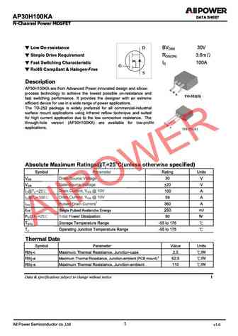

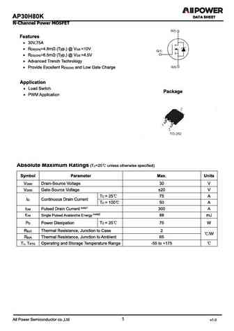

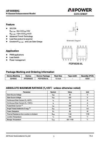
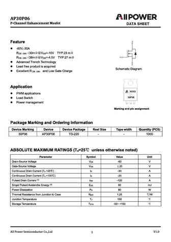

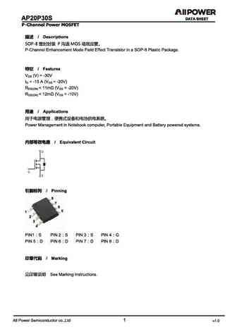
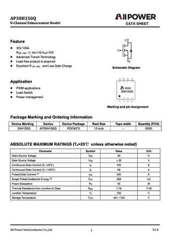
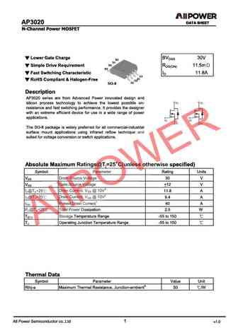
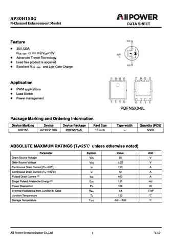
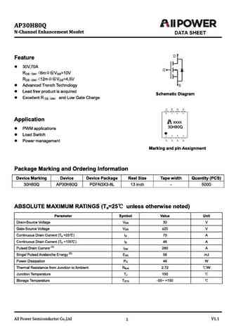
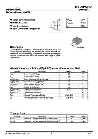
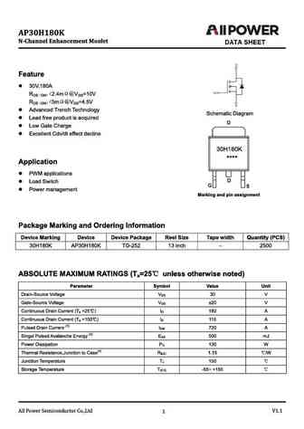
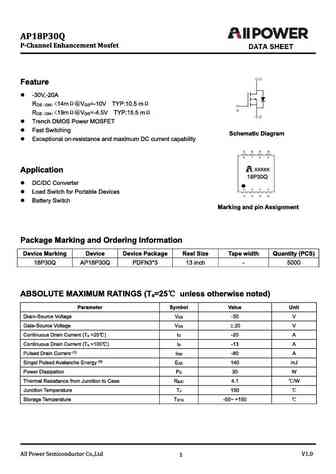
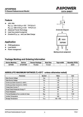
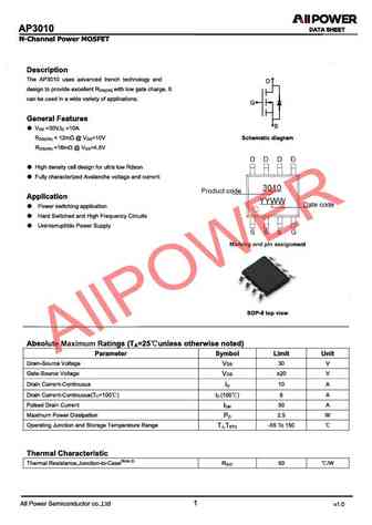
asdm30p30ctd.pdf
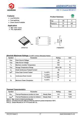
ASDM30P30CTD -30V P-Channel MOSFET Features Product Summary Low RDS(ON) Fast switching V -30 V DSS Green Device Available R 15 m DS(ON)-Typ. Application I -30 A D MB / VGA / Vcore POL Applications DFN3*3-8 P-MOSFET Absolute Maximum Ratings (T =25 C Unless Otherwise Noted) J Symbol Parameter Rating Unit VDSS Drain-Source Voltage -30 V VGSS Gate-
hsp3018b.pdf
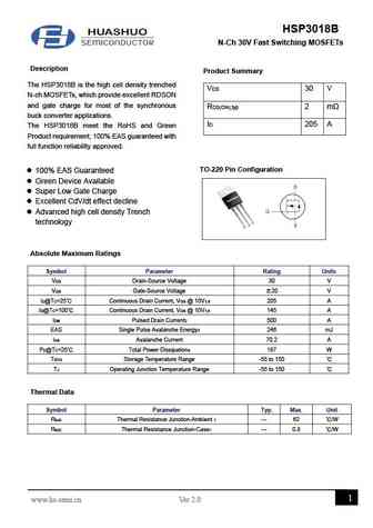
HSP3018B N-Ch 30V Fast Switching MOSFETs Description Product Summary The HSP3018B is the high cell density trenched VDS 30 V N-ch MOSFETs, which provide excellent RDSON and gate charge for most of the synchronous RDS(ON),typ 2 m buck converter applications. ID 205 A The HSP3018B meet the RoHS and Green Product requirement, 100% EAS guaranteed with full function reli
jmtp3008a.pdf
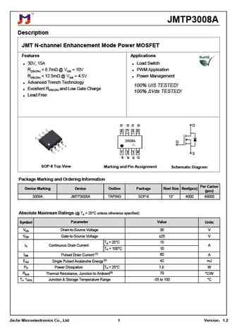
JMTP3008A Description JMT N-channel Enhancement Mode Power MOSFET Features Applications 30V, 15A Load Switch RDS(ON)
jmtp3010d.pdf
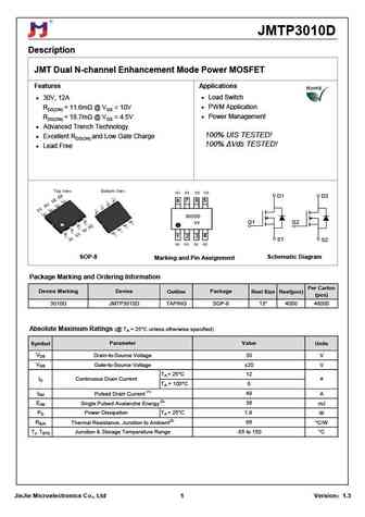
JMTP3010D Description JMT Dual N-channel Enhancement Mode Power MOSFET Features Applications 30V, 12A Load Switch RDS(ON)
tip3055.pdf
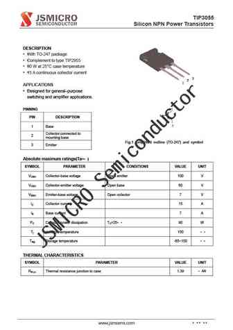
TIP3055 Silicon NPN Power Transistors DESCRIPTION With TO-247 package Complement to type TIP2955 90 W at 25 C case temperature 15 A continuous collector current APPLICATIONS Designed for general purpose switching and amplifier applications. PINNING PIN DESCRIPTION 1 Base Collector;connected to 2 mounting base Fig.1 simplified outline (TO-247) and symbol
agm40p30d.pdf
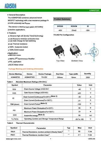
AGM40P30D General Description The AGM40P30D combines advanced trench Product Summary to MOSFET technology with a low resistance package provide extremely low R DS(ON) BVDSS RDSON ID This device is ideal and battery for load switch protection applications. -40V 25m -30A Features TO-252 Pin Configuration Advance high cell density Trench technology Low R to minimize
agm40p30ap.pdf
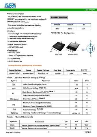
AGM40P30AP General Description The AGM40P30AP combines advanced trench Product Summary to MOSFET technology with a low resistance package provide extremely low R DS(ON) BVDSS RDSON ID This device is ideal and battery for load switch protection applications. -40V 26m -33A Features PDFN3.3*3.3 Pin Configuration Advance high cell density Trench technology Low R to mi
agm60p30ap.pdf
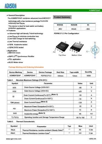
AGM60P30AP General Description Product Summary The AGM60P30AP combines advanced trench MOSFET to provide technology with a low resistance package extremely low R DS(ON) BVDSS RDSON ID This device is ideal for load switch and battery protection applications. -60V 40m -30A Features Advance high cell density Trench technology PDFN3.3*3.3 Pin Configuration Low R to mini
agm60p30c.pdf
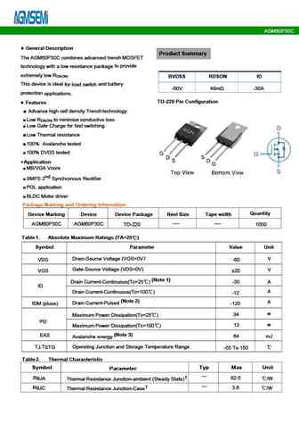
AGM60P30C Typical Characteristics (Cont.) Output Characteristics Drain-Source On Resistance 40 35 VGS= -5,-6,-7,-8,-9,-10V 35 -4V 30 30 VGS= -4.5V 25 25 20 20 15 10 VGS= -10V 15 5 -3V 0 10 0.0 0.5 1.0 1.5 2.0 2.5 3.0 0 10 20 30 40 -VDS - Drain-Source Voltage (V) -ID - Drain Current (A) Transfer Characteristics Normalized Threshold Voltage 60 1.8 IDS = -250 A ID
agm15p30as.pdf
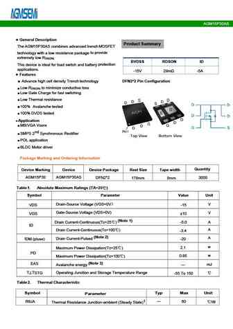
AGM15P30AS Table 3. Electrical Characteristics (TJ=25 unless otherwise noted) Symbol Parameter Conditions Min Typ Max Unit On/Off States BVDSS Drain-Source Breakdown Voltage V =0V I =-250 A -15 -18 -- V GS D Zero Gate Voltage Drain Current V =-15V,V =0V -- -- -1 A DS GS I DSS Gate-Body Leakage Current V = 10V,V =0V -- -- 100 nA GS DS I GSS VGS(th) Gate Threshold Voltag
agm40p30a.pdf
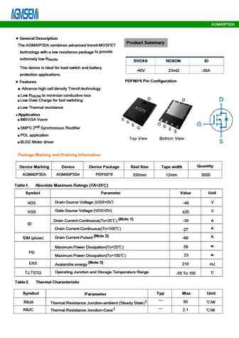
AGM40P30A Typical Characteristics -VDS,- Drain -Source Voltage (V) Tj - Junction Temperature ( C) Fig1. Typical Output Characteristics Fig2. -VGS(TH) Gate -Source Voltage Vs.Tj -VGS, -Gate -Source Voltage (V) Tj - Junction Temperature ( C) Fig3. Typical Transfer Characteristics Fig4. Normalized On-Resistance Vs. Tj -VSD, -Source-Drain Voltage (V) -VDS, -Drain -Source Voltage (V
agm15p30e.pdf
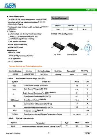
AGM15P30E General Description Product Summary The AGM15P30E combines advanced trench MOSFET to provide technology with a low resistance package extremely low R DS(ON) BVDSS RDSON ID protection This device is ideal for load switch and battery applications. -15V 34m -4.1A Features Advance high cell density Trench technology SOT-23-3 Pin Configuration Low R to minimize
agm60p30d.pdf
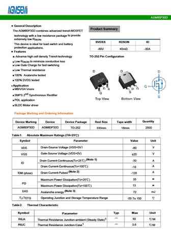
AGM60P30D Table 3. Electrical Characteristics (TJ=25 unless otherwise noted) Symbol Parameter Conditions Min Typ Max Unit On/Off States BVDSS Drain-Source Breakdown Voltage V =0V I =-250 A -60 -- -- V GS D Zero Gate Voltage Drain Current V =-60V,V =0V -- -- -1 A DS GS I DSS Gate-Body Leakage Current V = 20V,V =0V -- -- 100 nA GS DS I GSS VGS(th) Gate Threshold Voltage
agm60p30a.pdf
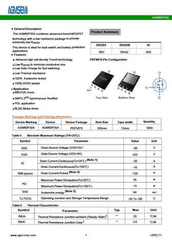
AGM60P30A General Description Product Summary The AGM60P30A combines advanced trench MOSFET to provide technology with a low resistance package extremely low R DS(ON) BVDSS RDSON ID protection This device is ideal for load switch and battery applications. -60V 50m -30A Features Advance high cell density Trench technology PDFN5*6 Pin Configuration Low R to minimize c
agm20p30ap1.pdf

AGM20P30AP1 Table 3. Electrical Characteristics (TJ=25 unless otherwise noted) Symbol Parameter Conditions Min Typ Max Unit On/Off States BV Drain-Source Breakdown Voltage V =0V I =250 A -20 -- -- V GS D DSS Zero Gate Voltage Drain Current V =-20V,V =0V -- -- -1.0 A DS GS I DSS V = 10V,V =0V -- -- nA GS DS IGSS Gate-Body Leakage Current 100 V Gate Threshold Voltage
agm20p30ap.pdf
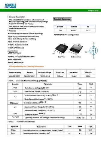
AGM20P30AP Typical Characteristics P-Ch 20V Fast Switching MOSFETs 20 ID=-14A 16 12 8 4 0 1 3 4 5 -VGS (V) Fig.1 Typical Output Characteristics Fig.2 On-Resistance vs. G-S Voltage 12 9 TJ=150 TJ=25 6 3 0 0 0.3 0.6 0.9 1.2 -VSD , Source-to-Drain Voltage (V) Fig.3 Forward Characteristics of Reverse Fig.4 Gate-charge Characteristics 1.8 1 . 8 1.4 1 . 4 1 1 . 0
sif30n60g21b sip30n60g21b siw30n60g21b sib30n60g21b.pdf
SUPER-SEMI Super Junction Insulated Gate Bipolar Transistor 600V Trench and Super Junction IGBT SI*30N60G21B Rev. 0.91 Jul. 2023 www.supersemi.com.cn SIF30N60G21B/SIP30N60G21B/SIW30N60G21B/ SIB30N60G21B 600V Trench and Super Junction IGBT General Description Super-Semi Trench and Super Junction IGBTs, VCE 600 V designed according to the super junction (SJ) IC 30 A technology. Th
sif30n65g21f sip30n65g21f siw30n65g21f sib30n65g21f.pdf

SUPER-SEMI Super Junction Insulated Gate Bipolar Transistor 650V Trench and Super Junction IGBT SI*30N65G21F Rev. 0.91 Jul. 2023 www.supersemi.com.cn SIF30N65G21F/SIP30N65G21F/SIW30N65G21F/ SIB30N65G21F 650V Trench and Super Junction IGBT General Description Super-Semi Trench and Super Junction IGBTs, VCE 650 V designed according to the super junction (SJ) IC 30 A technology. Th
dmp3098l.pdf
P-Channel Enhancement Mode MOSFET Channel Enhancement Mode MOSFET Feature -30V/-3.8A, RDS(ON) =55m (MAX) @VGS = -10V. 10V. RDS(ON) = 70m (MAX) @VGS = -4.5V. 4.5V. RDS(ON) =120m (MAX) @VGS = -2.5V. 2.5V. Super High dense cell design for extremely low R Super High dense cell design for extremely low RDS(ON) Reliable and Rugged SOT-23 for Surface Mount Package
sed30p30m.pdf
Sep 2015 SED30P30M P-Channel Enhancement-Mode MOSFET Revision A General Description Features Advanced trench technology to provide For a single MOSFET excellent RDS(ON), low gate charge and low V = -30V DS operation voltage. This device is suitable for R =8.5m @V =-10V DS(ON) GS using as a load switch or in PWM applications. Simple Drive Requirement Small Packa
stp30nf10.pdf
STP30NF10 www.VBsemi.tw N-Channel 100-V (D-S) MOSFET FEATURES PRODUCT SUMMARY TrenchFET Power MOSFETS V(BR)DSS (V) rDS(on) ( )ID (A) Available 175 C Junction Temperature 0.032 at VGS = 10 V 45 RoHS* 100 Low Thermal Resistance Package 0.035 at VGS = 4.5 V 40 COMPLIANT D TO-220AB G S G D S Top View N-Channel MOSFET ABSOLUTE MAXIMUM RATINGS TC = 25 C, u
dmp3010lps.pdf
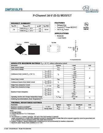
DMP3010LPS www.VBsemi.tw P-Channel 30-V (D-S) MOSFET FEATURES PRODUCT SUMMARY Halogen-free VDS (V) RDS(on) ( ) ID (A)a Qg (Typ.) TrenchFET Power MOSFET RoHS 0.004 at VGS = - 10 V - 120 COMPLIANT - 30 130 nC 100 % Rg Tested 0.006 at VGS = - 4.5 V - 100 APPLICATIONS Notebook - Load Switch S DFN5X6 Top View Top View Bottom View 1 8 G 2 7 3 6 4
stp30nf20.pdf
STP30NF20 www.VBsemi.tw N-Channel 200 V (D-S) MOSFET FEATURES PRODUCT SUMMARY TrenchFET Power MOSFETS VDS (V) RDS(on) ( ) ID (A) Qg (Typ) 175 C Junction Temperature RoHS 0.060 at VGS = 10 V COMPLIANT 40 New Low Thermal Resistance Package 200 95 0.070 at VGS = 6 V 38.7 Compliant to RoHS Directive 2002/95/EC APPLICATIONS TO-220AB Industrial D G
vbc6p3033.pdf
VBC6P3033 www.VBsemi.com Dual P-Channel 30-V (D-S) MOSFET FEATURES PRODUCT SUMMARY Halogen-free VDS (V) RDS(on) ( )ID (A) TrenchFET Power MOSFETs 0.036 at VGS = - 10 V - 5.2 - 30 RoHS 0.055 at VGS = - 4.5 V - 4.2 COMPLIANT APPLICATIONS Load Switch Battery Switch S1 S2 TSSOP-8 G1 G2 D1 1 D2 8 S1 2 S2 7 S1 3 S2 6 G1 4 G2 5 Top View D1 D2
fqp30n06l.pdf
FQP30N06L www.VBsemi.tw N-Channel 60 V (D-S) MOSFET FEATURES PRODUCT SUMMARY Halogen-free According to IEC 61249-2-21 VDS (V) RDS(on) ( ) ID (A)a, e Qg (Max) Definition Surface Mount 0.024 at VGS = 10 V 50 60 66 nC Available in Tape and Reel 0.028 at VGS = 4.5 V 40 Dynamic dV/dt Rating Logic-Level Gate Drive Fast Switching Compliant to RoHS Di
dmp3056lsd-13.pdf
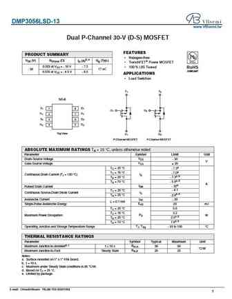
DMP3056LSD-13 www.VBsemi.tw Dual P-Channel 30-V (D-S) MOSFET FEATURES PRODUCT SUMMARY Halogen-free VDS (V) RDS(on) ( ) ID (A)d, e Qg (Typ.) TrenchFET Power MOSFET 0.029 at VGS = - 10 V - 7.3 100 % UIS Tested RoHS - 30 17 nC COMPLIANT 0.039 at VGS = - 4.5 V - 6.3 APPLICATIONS Load Switches S1 S2 SO-8 S1 1 D1 8 G1 G2 G1 2 D1 7 S2 3 D2 6 G2 4 D2 5 To
stp30nf10fp.pdf
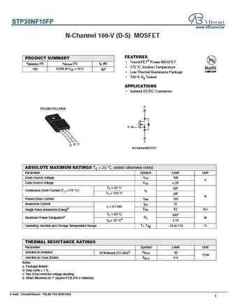
STP30NF10FP www.VBsemi.tw N-Channel 100-V (D-S) MOSFET FEATURES PRODUCT SUMMARY TrenchFET Power MOSFET V(BR)DSS (V) rDS(on) ( )ID (A) 175 C Junction Temperature RoHS 0.034 at VGS = 10 V 100 50a COMPLIANT Low Thermal Resistance Package 100 % Rg Tested APPLICATIONS Isolated DC/DC Converters D TO-220 FULLPAK G S S D G N-Channel MOSFET ABSOLUTE MA
rfp30p06.pdf
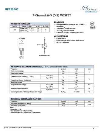
RFP30P06 www.VBsemi.tw P-Channel 60 V (D-S) MOSFET FEATURES PRODUCT SUMMARY Halogen-free According to IEC 61249-2-21 VDS (V) RDS(on) ( ) Max. ID (A) Qg (Typ.) Definition TrenchFET Power MOSFET 0.0600 at VGS = - 10 V - 30 - 60 67 100 % Rg and UIS Tested 0.0850 at VGS = - 4.5 V - 24 Compliant to RoHS Directive 2002/95/EC APPLICATIONS S TO-220AB Power Swi
p3055ldg.pdf
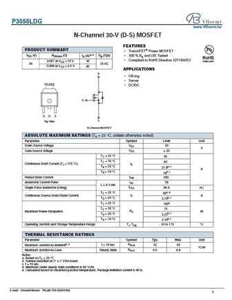
P3055LDG www.VBsemi.tw N-Channel 30-V (D-S) MOSFET FEATURES PRODUCT SUMMARY TrenchFET Power MOSFET VDS (V) RDS(on) ( ) ID (A)a, e Qg (Typ) 100 % Rg and UIS Tested Compliant to RoHS Directive 2011/65/EU 0.007 at VGS = 10 V 50 30 25 nC 0.009 at VGS = 4.5 V 40 APPLICATIONS D OR-ing Server TO-252 DC/DC G G D S S Top View N-Channel MOSFET ABSOL
dmp3025lk3-13.pdf
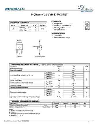
DMP3025LK3-13 www.VBsemi.tw P-Channel 30-V (D-S) MOSFET FEATURES PRODUCT SUMMARY Halogen-free VDS (V) RDS(on) ( ) ID (A)d Qg (Typ.) TrenchFET Power MOSFET 0.033 at VGS = - 10 V - 26 100 % Rg Tested RoHS - 30 19 nC COMPLIANT 100 % UIS Tested 0.046 at VGS = - 4.5 V - 21 APPLICATIONS Load Switch Notebook Adaptor Switch S TO-252 G G D S D Top View
rfp30n06le.pdf
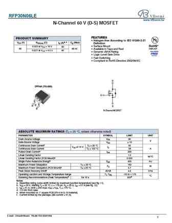
RFP30N06LE www.VBsemi.tw N-Channel 60 V (D-S) MOSFET FEATURES PRODUCT SUMMARY Halogen-free According to IEC 61249-2-21 VDS (V) RDS(on) ( ) ID (A)a, e Qg (Max) Definition Surface Mount 0.023 at VGS = 10 V 50 60 66 nC Available in Tape and Reel 0.027 at VGS = 4.5 V 40 Dynamic dV/dt Rating Logic-Level Gate Drive Fast Switching Compliant to RoHS D
ttd30p10at ttp30p10at.pdf
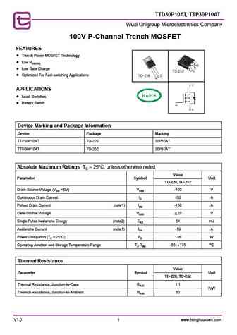
TTD30P10AT, TTP30P10AT Wuxi Unigroup Microelectronics Company 100V P-Channel Trench MOSFET FEATURES Trench Power MOSFET Technology Low RDS(ON) Low Gate Charge Optimized For Fast-switching Applications APPLICATIONS Load Switches Battery Switch Device Marking and Package Information Device Package Marking TTP30P10AT TO-220 30P10AT TTD30P10AT TO
ttb30p10at ttd30p10at ttp30p10at.pdf
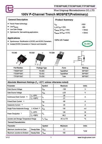
TTB30P10AT,TTD30P10AT,TTP30P10AT Wuxi Unigroup Microelectronics CO.,LTD. 100V P-Channel Trench MOSFET(Preliminary) General Description Product Summary Trench Power technology VDS -100V Low RDS(ON) ID (at VGS =-10V) -30A Low Gate Charge RDS(ON) (at VGS =-10V)
dmp3028lk3.pdf

isc P-Channel MOSFET Transistor DMP3028LK3 FEATURES Drain Current I = -27A@ T =25 D C Drain Source Voltage- V = -30V(Min) DSS Static Drain-Source On-Resistance R = 25m (Max) DS(on) 100% avalanche tested Minimum Lot-to-Lot variations for robust device performance and reliable operation DESCRIPTION Designed for use in switch mode power supplies and general pu
tip3055.pdf
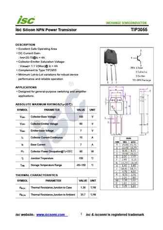
INCHANGE Semiconductor isc Silicon NPN Power Transistor TIP3055 DESCRIPTION Excellent Safe Operating Area DC Current Gain- h =20-70@I = 4A FE C Collector-Emitter Saturation Voltage- V )= 1.1 V(Max)@ I = 4A CE(sat C Complement to Type TIP2955 Minimum Lot-to-Lot variations for robust device performance and reliable operation APPLICATIONS Designed for general-purpose
stp30nf10.pdf
Isc N-Channel MOSFET Transistor STP30NF10 FEATURES Typical R (on)=0.038 DS Application oriented characterization Easy to drive 100% avalanche tested Minimum Lot-to-Lot variations for robust device performance and reliable operation APPLICATIONS High-efficiency DC-DC coverters Motor control ABSOLUTE MAXIMUM RATINGS(T =25 ) a SYMBOL PARAMETER VALUE UNIT V Dr
irfp3077.pdf
isc N-Channel MOSFET Transistor IRFP3077 IIRFP3077 FEATURES Static drain-source on-resistance RDS(on) 3.3m Enhancement mode 100% avalanche tested Minimum Lot-to-Lot variations for robust device performance and reliable operation DESCRITION High Efficiency Synchronous Rectification in SMPS Uninterruptible Power Supply High Speed Power Switching Hard Switc
tip30a.pdf
isc Silicon PNP Power Transistors TIP30A DESCRIPTION Collector-Emitter Sustaining Voltage- V = -60V(Min) CEO(SUS) Collector-Emitter Saturation Voltage- V = -0.7V(Max.)@I = -1.0A CE(sat) C Complement to Type TIP29A Minimum Lot-to-Lot variations for robust device performance and reliable operation APPLICATIONS Designed for use in general purpose amplifier and switching
stp30nf20.pdf
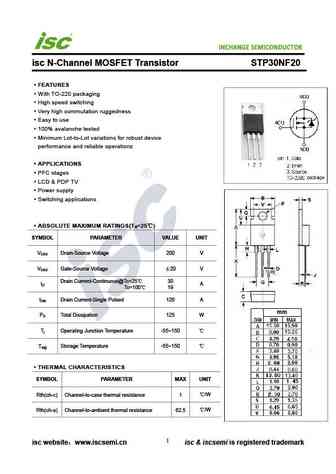
INCHANGE Semiconductor isc N-Channel MOSFET Transistor STP30NF20 FEATURES With TO-220 packaging High speed switching Very high commutation ruggedness Easy to use 100% avalanche tested Minimum Lot-to-Lot variations for robust device performance and reliable operationz APPLICATIONS PFC stages LCD & PDP TV Power supply Switching applications ABSOLUTE MAXIMU
dmp3010lk3.pdf
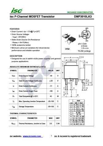
isc P-Channel MOSFET Transistor DMP3010LK3 FEATURES Drain Current I = -17A@ T =25 D C Drain Source Voltage- V = -30V(Min) DSS Static Drain-Source On-Resistance R = 8m (Max) DS(on) 100% avalanche tested Minimum Lot-to-Lot variations for robust device performance and reliable operation DESCRIPTION Designed for use in switch mode power supplies and general pur
irfp3006.pdf
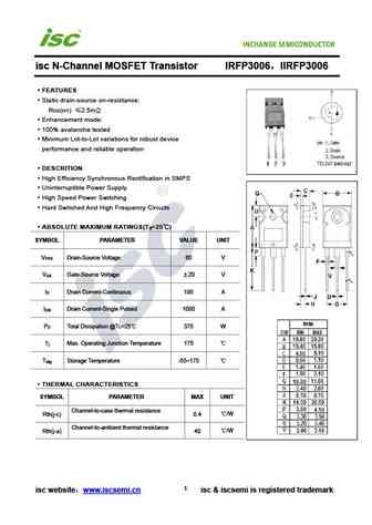
isc N-Channel MOSFET Transistor IRFP3006 IIRFP3006 FEATURES Static drain-source on-resistance RDS(on) 2.5m Enhancement mode 100% avalanche tested Minimum Lot-to-Lot variations for robust device performance and reliable operation DESCRITION High Efficiency Synchronous Rectification in SMPS Uninterruptible Power Supply High Speed Power Switching Hard Swit
tip3055t.pdf
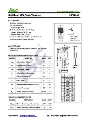
isc Silicon NPN Power Transistor TIP3055T DESCRIPTION Excellent Safe Operating Area DC Current Gain- h =20-70@I = 4A FE C Collector-Emitter Saturation Voltage- V )= 0.8V(Max)@ I = 4A CE(sat C Complement to Type TIP2955T Minimum Lot-to-Lot variations for robust device performance and reliable operation APPLICATIONS Designed for general-purpose switching and amplifier
stp30nf10fp.pdf
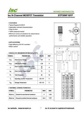
INCHANGE Semiconductor Isc N-Channel MOSFET Transistor STP30NF10FP FEATURES Typical R (on)=0.038 DS Application oriented characterization Easy to drive 100% avalanche tested Minimum Lot-to-Lot variations for robust device performance and reliable operation APPLICATIONS High-efficiency DC-DC coverters Motor control ABSOLUTE MAXIMUM RATINGS(T =25 ) a SYMBOL
tip30.pdf
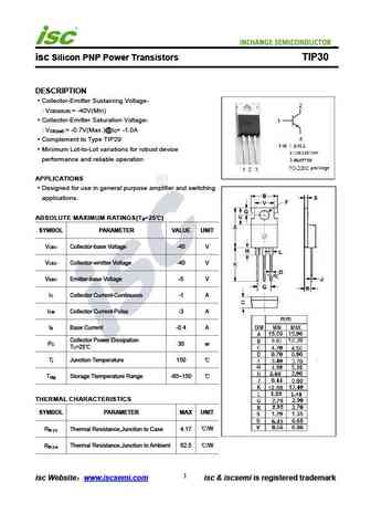
isc Silicon PNP Power Transistors TIP30 DESCRIPTION Collector-Emitter Sustaining Voltage- V = -40V(Min) CEO(SUS) Collector-Emitter Saturation Voltage- V = -0.7V(Max.)@I = -1.0A CE(sat) C Complement to Type TIP29 Minimum Lot-to-Lot variations for robust device performance and reliable operation APPLICATIONS Designed for use in general purpose amplifier and switching ap
tip30 tip30a tip30b tip30c.pdf
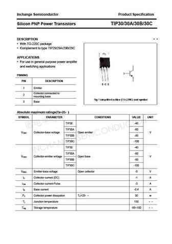
Inchange Semiconductor Product Specification Silicon PNP Power Transistors TIP30/30A/30B/30C DESCRIPTION With TO-220C package Complement to type TIP29/29A/29B/29C APPLICATIONS For use in general purpose power amplifer and switching applications PINNING PIN DESCRIPTION 1 Emitter Collector;connected to 2 mounting base 3 Base Absolute maximum ratings(Ta=25 )
irlp3034.pdf
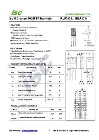
INCHANGE Semiconductor isc N-Channel MOSFET Transistor IRLP3034 IIRLP3034 FEATURES Static drain-source on-resistance RDS(on) 1.7m Enhancement mode Vth =1.0 to 2.5V (VDS=VGS, ID=250 A) 100% avalanche tested Minimum Lot-to-Lot variations for robust device performance and reliable operation DESCRITION High Efficiency Synchronous Rectification in SMPS Uninterru
tip30c.pdf
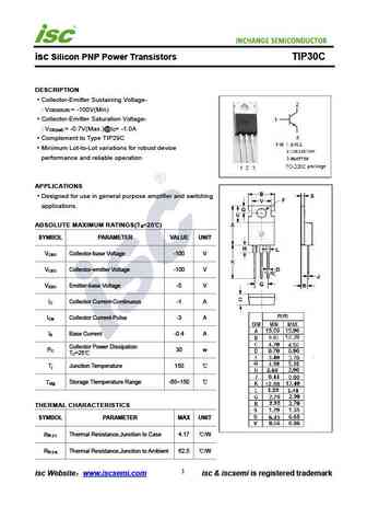
isc Silicon PNP Power Transistors TIP30C DESCRIPTION Collector-Emitter Sustaining Voltage- V = -100V(Min) CEO(SUS) Collector-Emitter Saturation Voltage- V = -0.7V(Max.)@I = -1.0A CE(sat) C Complement to Type TIP29C Minimum Lot-to-Lot variations for robust device performance and reliable operation APPLICATIONS Designed for use in general purpose amplifier and switching
tip30b.pdf
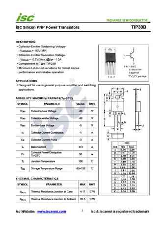
isc Silicon PNP Power Transistors TIP30B DESCRIPTION Collector-Emitter Sustaining Voltage- V = -80V(Min) CEO(SUS) Collector-Emitter Saturation Voltage- V = -0.7V(Max.)@I = -1.0A CE(sat) C Complement to Type TIP29B Minimum Lot-to-Lot variations for robust device performance and reliable operation APPLICATIONS Designed for use in general purpose amplifier and switching
bup30.pdf
INCHANGE Semiconductor isc Silicon NPN Power Transistors BUP30 DESCRIPTION Low Collector Saturation Voltage V = 0.4V(Max)@ I =6A CE(sat) C Minimum Lot-to-Lot variations for robust device performance and reliable operation APPLICATIONS Designed for relay drivers, high-speed inverters, converters, and other general high-current switching applications ABSOLUTE MAXIMUM RATINGS(T
fkp300a.pdf
isc N-Channel MOSFET Transistor FKP300A FEATURES Drain Current I =30A@ T =25 D C Drain Source Voltage- V =300V(Min) DSS Static Drain-Source On-Resistance R = 65m (Max) DS(on) 100% avalanche tested Minimum Lot-to-Lot variations for robust device performance and reliable operation DESCRIPTION Designed for use in switch mode power supplies and general purpose
ap30h04df.pdf
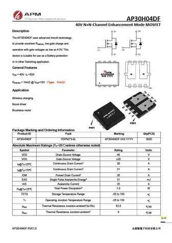
AP30H04DF 40V N+N-Channel Enhancement Mode MOSFET Description The AP30H04DF uses advanced trench technology to provide excellent R , low gate charge and DS(ON) operation with gate voltages as low as 4.5V. This device is suitable for use as a Battery protection or in other Switching application. General Features V = 40V I =30A DS D R
ap30n06df.pdf
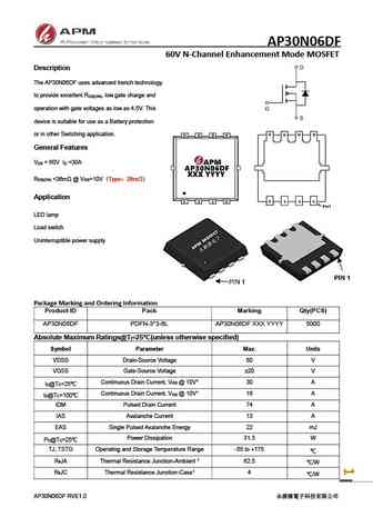
AP30N06DF 60V N-Channel Enhancement Mode MOSFET Description The AP30N06DF uses advanced trench technology to provide excellent R , low gate charge and DS(ON) operation with gate voltages as low as 4.5V. This device is suitable for use as a Battery protection or in other Switching application. General Features V = 60V I =30A DS D R
ap30n06y.pdf
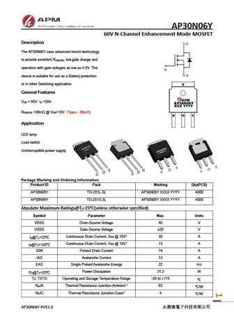
AP30N06Y 60V N-Channel Enhancement Mode MOSFET Description The AP30N06Y uses advanced trench technology to provide excellent R , low gate charge and DS(ON) operation with gate voltages as low as 4.5V. This device is suitable for use as a Battery protection or in other Switching application. General Features V = 60V I =30A DS D R
ap30p03df.pdf
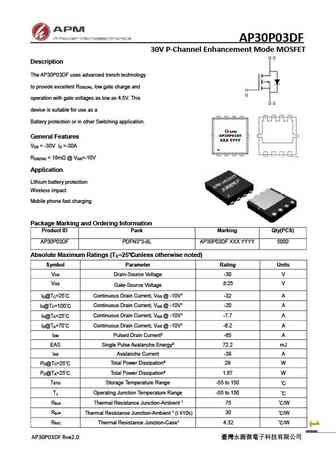
AP30P03DF 30V P-Channel Enhancement Mode MOSFET Description The AP30P03DF uses advanced trench technology to provide excellent R , low gate charge and DS(ON) operation with gate voltages as low as 4.5V. This device is suitable for use as a Battery protection or in other Switching application. General Features V = -30V I =-30A DS D R
ap30g03gd.pdf
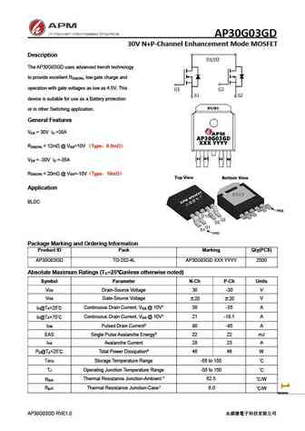
AP30G03GD 30V N+P-Channel Enhancement Mode MOSFET Description The AP30G03GD uses advanced trench technology to provide excellent R , low gate charge and DS(ON) operation with gate voltages as low as 4.5V. This device is suitable for use as a Battery protection or in other Switching application. General Features V = 30V I =38A DS D R
ap30p10d.pdf

AP30P10D -100V P-Channel Enhancement Mode MOSFET Description The AP30P10P uses advanced trench technology to provide excellent R , low gate charge and DS(ON) operation with gate voltages as low as 4.5V. This device is suitable for use as a Battery protection or in other Switching application. General Features V = -100V I =-30A DS D R
ap30n06p ap30n06t.pdf
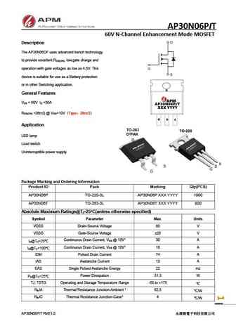
AP30N06PIT 60V N-Channel Enhancement Mode MOSFET Description The AP30N06DF uses advanced trench technology to provide excellent R , low gate charge and DS(ON) operation with gate voltages as low as 4.5V. This device is suitable for use as a Battery protection or in other Switching application. General Features V = 60V I =30A DS D R
ap300n04tlg5.pdf
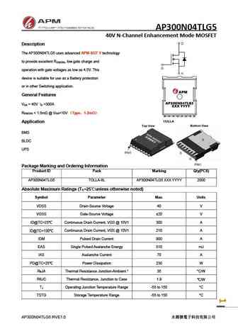
AP300N04TLG5 40V N-Channel Enhancement Mode MOSFET Description The AP300N04TLG5 uses advanced APM-SGT V technology to provide excellent R , low gate charge and DS(ON) operation with gate voltages as low as 4.5V. This device is suitable for use as a Battery protection or in other Switching application. General Features V = 40V I =300A DS D R
ap30p10p.pdf
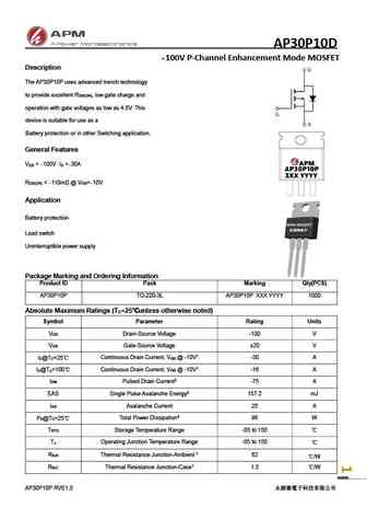
AP30P10D -100V P-Channel Enhancement Mode MOSFET Description The AP30P10P uses advanced trench technology to provide excellent R , low gate charge and DS(ON) operation with gate voltages as low as 4.5V. This device is suitable for use as a Battery protection or in other Switching application. General Features V = -100V I =-30A DS D R
ap30n10y.pdf
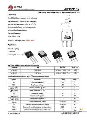
AP30N10Y 100V N-Channel Enhancement Mode MOSFET Description The AP30N10D uses advanced trench technology to provide excellent R , low gate charge and DS(ON) operation with gate voltages as low as 4.5V. This device is suitable for use as a Battery protection or in other Switching application. General Features V = 100V I =30A DS D R
ap30p03d.pdf
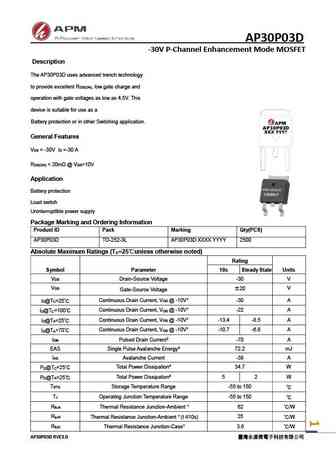
AP30P03D -30V P-Channel Enhancement Mode MOSFET Electrical Characteristics (TJ=25 , unless otherwise noted) Symbol Parameter Conditions Min. Typ. Max. Unit BVDSS Drain-Source Breakdown Voltage V =0V , I =-250uA -30 --- --- V GS D BVDSS/ TJ BV Temperature Coefficient DSS Reference to 25 , I =-1mA --- -0.022 --- D V/ V =-10V , I =-15A --- 18 20 GS D m RDS(O
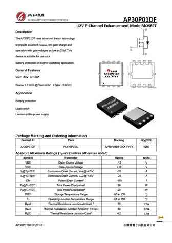
ap30n10d.pdf
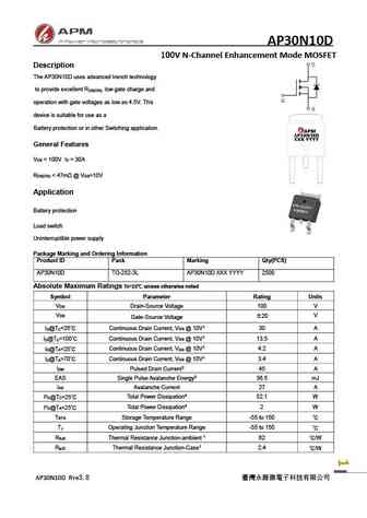
AP30N10D 100V N-Channel Enhancement Mode MOSFET Description The AP30N10D uses advanced trench technology to provide excellent R , low gate charge and DS(ON) operation with gate voltages as low as 4.5V. This device is suitable for use as a Battery protection or in other Switching application. General Features V = 100V I = 30A DS D R
ap30p02df.pdf
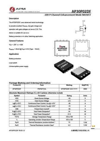
AP30P02DF -20V P-Channel Enhancement Mode MOSFET Description The AP30P02DF uses advanced trench technology to provide excellent R , low gate charge and DS(ON) operation with gate voltages as low as 2.5V. This device is suitable for use as a Battery protection or in other Switching application. General Features V = -20V I =-30A DS D R
ap30n03df.pdf
AP30N03DF 30V N-Channel Enhancement Mode MOSFET Description The AP30N03DF uses advanced trench technology to provide excellent R , low gate charge and DS(ON) operation with gate voltages as low as 4.5V. This device is suitable for use as a Battery protection or in other Switching application. General Features V = 30V I =30 A DS D R
ap30h04nf.pdf
AP30H04NF 40V N+N-Channel Enhancement Mode MOSFET Description The AP30H04NF uses advanced trench technology to provide excellent R , low gate charge and DS(ON) operation with gate voltages as low as 4.5V. This device is suitable for use as a Battery protection or in other Switching application. General Features V = 40V I =30A DS D R
ap30p06d.pdf
AP30P06D -60V P-Channel Enhancement Mode MOSFET Description The AP30P06D uses advanced trench technology to provide excellent R , low gate charge and DS(ON) operation with gate voltages as low as 4.5V. This device is suitable for use as a Battery protection or in other Switching application. General Features V = -60V I =-30A DS D R
ap30n20p.pdf
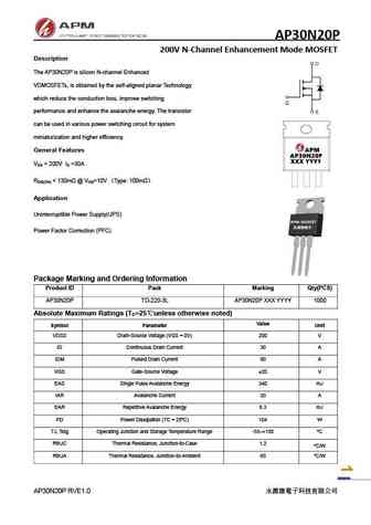
AP30N20P 200V N-Channel Enhancement Mode MOSFET Description The AP30N20P is silicon N-channel Enhanced VDMOSFETs, is obtained by the self-aligned planar Technology which reduce the conduction loss, improve switching performance and enhance the avalanche energy. The transistor can be used in various power switching circuit for system miniaturization and higher efficiency. Gener
ap30n06d.pdf
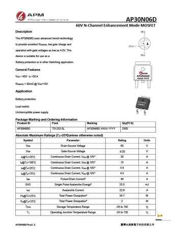
AP30N06D 60V N-Channel Enhancement Mode MOSFET Description The AP30N06D uses advanced trench technology to provide excellent R , low gate charge and DS(ON) operation with gate voltages as low as 4.5V. This device is suitable for use as a Battery protection or in other Switching application. General Features V = 60V I =30 A DS D R
ap30n02d.pdf
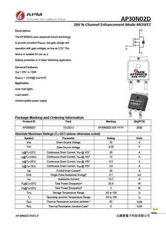
AP30N02D 20V N-Channel Enhancement Mode MOSFET Description The AP30N02D uses advanced trench technology to provide excellent R , low gate charge and DS(ON) operation with gate voltages as low as 2.5V. This device is suitable for use as a Battery protection or in other Switching application. General Features V = 20V I =30A DS D R = 11m @ V =4.5V DS(ON) GS Application
ap30n15d.pdf
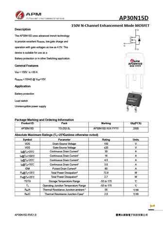
AP30N15D 150V N-Channel Enhancement Mode MOSFET Description The AP30N15D uses advanced trench technology to provide excellent R , low gate charge and DS(ON) operation with gate voltages as low as 4.5V. This device is suitable for use as a Battery protection or in other Switching application. General Features V = 150V I =30 A DS D R
Другие транзисторы: P217B, P217G, P217V, P27, P27A, P28, P29, P29A, 2SC828, P302, P303, P303A, P304, P306, P306A, P307, P307A
History: KTA1040L
🌐 : EN ES РУ

Список транзисторов
Обновления
BJT: GA1A4M | SBT42 | 2SA200-Y | 2SA200-O | 2SD882-Q | 2SD882-P | 2SD882-E | 2SC945-L | 2SC945-H | 2SC4226-R23 | 2SC3357-F | 2SC3357-E | 2SC3356-R26 | 2SC3356-R24 | 2SC3356-R23 | 2SB772-Q | 2SB772-P | 2SB772-E | 2SA1015-L | 2SA1015-H | HSS8550
Popular searches
2sa679 | 2sc3181 | 2sb324 | 2sc1904 | 2sc281 | m28s transistor | 2n3640 | tta1943 transistor