P605 datasheet, аналоги, основные параметры
Наименование производителя: P605 📄📄
Тип материала: Ge
Полярность: PNP
Предельные значения
Максимальная рассеиваемая мощность (Pc): 3 W
Макcимально допустимое напряжение коллектор-база (Ucb): 45 V
Макcимально допустимое напряжение эмиттер-база (Ueb): 1 V
Макcимальный постоянный ток коллектора (Ic): 1.5 A
Предельная температура PN-перехода (Tj): 75 °C
Электрические характеристики
Граничная частота коэффициента передачи тока (ft): 45 MHz
Ёмкость коллекторного перехода (Cc): 130 pf
Статический коэффициент передачи тока (hFE): 20
Аналоги (замена) для P605
- подборⓘ биполярного транзистора по параметрам
P605 даташит
0.2. Size:377K diodes
dmp6050ssd.pdf 
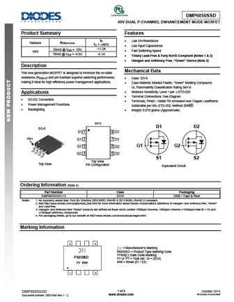
DMP6050SSD 60V DUAL P-CHANNEL ENHANCEMENT MODE MOSFET Product Summary Features ID Low On-Resistance V(BR)DSS RDS(on) max TC = +25 C Low Input Capacitance -11.3A 55m @ VGS = -10V Fast Switching Speed -60V -9.1A 70m @ VGS = -4.5V Totally Lead-Free & Fully RoHS Compliant (Notes 1 & 2) Halogen and Antimony Free. Green Device (Note 3) De
0.3. Size:551K diodes
dmp6050sfg.pdf 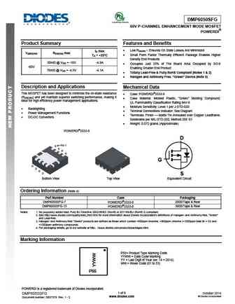
DMP6050SFG 60V P-CHANNEL ENHANCEMENT MODE MOSFET POWERDI Product Summary Features and Benefits Low RDS(ON) Ensures On State Losses Are Minimized ID max V(BR)DSS RDS(ON) max Small Form Factor Thermally Efficient Package Enables Higher TA = +25 C Density End Products 50m @ VGS = -10V -4.8A Occupies Just 33% of The Board Area Occupied by SO-8 -60V
0.5. Size:629K cet
cep6056 ceb6056.pdf 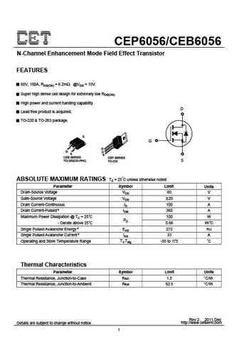
CEP6056/CEB6056 N-Channel Enhancement Mode Field Effect Transistor FEATURES 60V, 100A, RDS(ON) = 6.2m @VGS = 10V. Super high dense cell design for extremely low RDS(ON). High power and current handing capability. D Lead free product is acquired. TO-220 & TO-263 package. G CEB SERIES CEP SERIES TO-263(DD-PAK) S TO-220 ABSOLUTE MAXIMUM RATINGS Tc = 25 C unless otherwise noted Pa
0.6. Size:579K aosemi
aop605.pdf 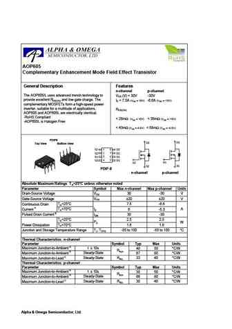
AOP605 Complementary Enhancement Mode Field Effect Transistor General Description Features n-channel p-channel The AOP605/L uses advanced trench technology to VDS (V) = 30V -30V provide excellent RDS(ON) and low gate charge. The ID = 7.5A (VGS = 10V) -6.6A (VGS = -10V) complementary MOSFETs form a high-speed power inverter, suitable for a multitude of applications. RDS(ON) AOP605 and
0.7. Size:556K ncepower
ncep6050qu.pdf 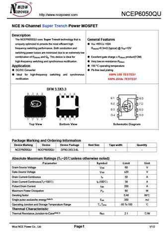
http //www.ncepower.com NCEP6050QU NCE N-Channel Super Trench Power MOSFET Description The NCEP6050QU uses Super Trench technology that is General Features uniquely optimized to provide the most efficient high V =60V,I =50A DS D frequency switching performance. Both conduction and R =6.5m (typical) @ V =10V DS(ON) GS switching power losses are minimized due to an extremely low c
0.8. Size:759K ncepower
nceap6055agu.pdf 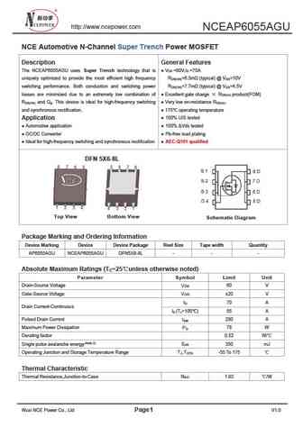
http //www.ncepower.com NCEAP6055AGU NCE Automotive N-Channel Super Trench Power MOSFET Description General Features The NCEAP6055AGU uses Super Trench technology that is V =60V,I =70A DS D uniquely optimized to provide the most efficient high frequency R =6.5m (typical) @ V =10V DS(ON) GS switching performance. Both conduction and switching power R =7.7m (typical) @ V =4.5V DS
0.9. Size:648K ncepower
ncep6055gu.pdf 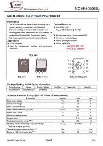
http //www.ncepower.com NCEP6055GU NCE N-Channel Super Trench Power MOSFET Description The NCEP6055GU uses Super Trench technology that is General Features uniquely optimized to provide the most efficient high V =60V,I =55A DS D frequency switching performance. Both conduction and R =6.5m (typical) @ V =10V DS(ON) GS switching power losses are minimized due to an extremely low c
0.10. Size:698K ncepower
nceap6050aqu.pdf 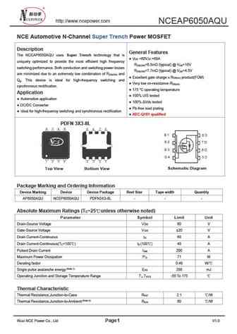
http //www.ncepower.com NCEAP6050AQU NCE Automotive N-Channel Super Trench Power MOSFET Description General Features The NCEAP6050AQU uses Super Trench technology that is V =60V,I =68A DS D uniquely optimized to provide the most efficient high frequency R =6.5m (typical) @ V =10V DS(ON) GS switching performance. Both conduction and switching power losses R =7.7m (typical) @
0.11. Size:630K ncepower
ncep6050aqu.pdf 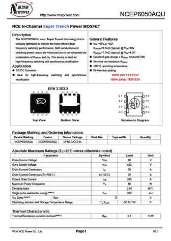
http //www.ncepower.com NCEP6050AQU NCE N-Channel Super Trench Power MOSFET Description The NCEP6050AQU uses Super Trench technology that is General Features uniquely optimized to provide the most efficient high V =60V,I =50A DS D frequency switching performance. Both conduction and R =6.5m (typical) @ V =10V DS(ON) GS switching power losses are minimized due to an extremely low
0.12. Size:1005K ncepower
ncep6055agu.pdf 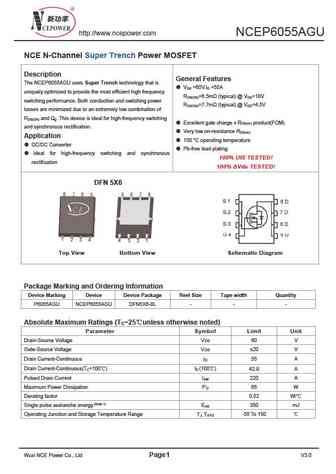
http //www.ncepower.com NCEP6055AGU NCE N-Channel Super Trench Power MOSFET Description General Features The NCEP6055AGU uses Super Trench technology that is V =60V,I =55A DS D uniquely optimized to provide the most efficient high frequency R =6.5m (typical) @ V =10V DS(ON) GS switching performance. Both conduction and switching power R =7.7m (typical) @ V =4.5V DS(ON) GS l
0.13. Size:962K stansontech
stp605d.pdf 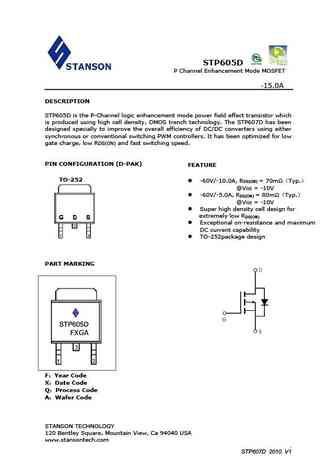
STP605D P Channel Enhancement Mode MOSFET -15.0A DESCRIPTION STP605D is the P-Channel logic enhancement mode power field effect transistor which is produced using high cell density, DMOS trench technology. The STP607D has been designed specially to improve the overall efficiency of DC/DC converters using either synchronous or conventional switching PWM controllers. It has been
0.14. Size:261K inchange semiconductor
ndp6051.pdf 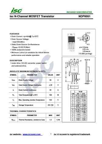
isc N-Channel MOSFET Transistor NDP6051 FEATURES Drain Current I =48A@ T =25 D C Drain Source Voltage- V =50V(Min) DSS Static Drain-Source On-Resistance R =0.022 (Max) DS(on) 100% avalanche tested Minimum Lot-to-Lot variations for robust device performance and reliable operation DESCRIPTION motor drive, DC-DC converter, power switch and solenoid drive. ABS
Другие транзисторы: P416A, P416B, P417, P417A, P417B, P422, P423, P6009, C5198, P605A, P606, P606A, P607, P607A, P608, P608A, P609