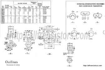
2N56. Аналоги и основные параметры
Наименование производителя: 2N56
Тип материала: Ge
Полярность: PNP
Предельные значения
Максимальная рассеиваемая мощность (Pc): 0.2 W
Макcимально допустимое напряжение коллектор-база (Ucb): 60 V
Макcимальный постоянный ток коллектора (Ic): 0.01 A
Предельная температура PN-перехода (Tj): 60 °C
Электрические характеристики
Граничная частота коэффициента передачи тока (ft): 0.5 MHz
Статический коэффициент передачи тока (hFE): 9
Корпус транзистора: TO50-3
Аналоги (замена) для 2N56
- подборⓘ биполярного транзистора по параметрам
2N56 даташит
2n5684 2n5685 2n5686.pdf
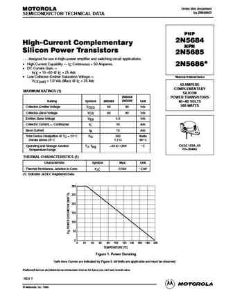
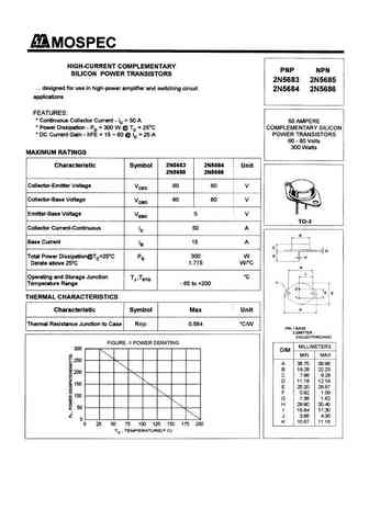
Order this document MOTOROLA by 2N5684/D SEMICONDUCTOR TECHNICAL DATA PNP 2N5684 High-Current Complementary NPN Silicon Power Transistors 2N5685 . . . designed for use in high power amplifier and switching circuit applications. High Current Capability IC Continuous = 50 Amperes. * 2N5686 DC Current Gain hFE = 15 60 @ IC = 25 Adc Low Collector Emitter Sa
2n5640.pdf
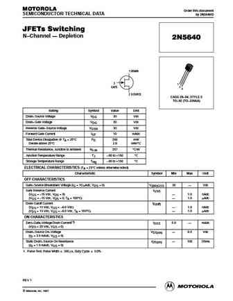
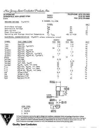
MOTOROLA Order this document SEMICONDUCTOR TECHNICAL DATA by 2N5640/D JFETs Switching N Channel Depletion 2N5640 1 DRAIN 3 1 GATE 2 3 2 SOURCE CASE 29 04, STYLE 5 TO 92 (TO 226AA) Rating Symbol Value Unit Drain Source Voltage VDS 30 Vdc Drain Gate Voltage VDG 30 Vdc Reverse Gate Source Voltage VGSR 30 Vdc Forward Gate Current IGF 10 mAdc Total Device Dissip
2n5655-57 2n5655 2n5656 2n5657.pdf
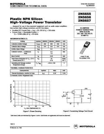
Order this document MOTOROLA by 2N5655/D SEMICONDUCTOR TECHNICAL DATA 2N5655 2N5656 Plastic NPN Silicon 2N5657 High-Voltage Power Transistor . . . designed for use in line operated equipment such as audio output amplifiers; low current, high voltage converters; and AC line relays. 0.5 AMPERE POWER TRANSISTORS Excellent DC Current Gain hFE = 30 250 @ IC = 100 mAdc NP
2n5630 2n6030 2n5631 2n6031.pdf
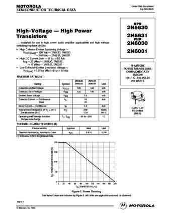
Order this document MOTOROLA by 2N5630/D SEMICONDUCTOR TECHNICAL DATA NPN 2N5630 High-Voltage High Power 2N5631 Transistors PNP . . . designed for use in high power audio amplifier applications and high voltage 2N6030 switching regulator circuits. High Collector Emitter Sustaining Voltage 2N6031 VCEO(sus) = 120 Vdc 2N5630, 2N6030 VCEO(sus) = 140 Vdc 2N5631, 2N603
2n5657.pdf
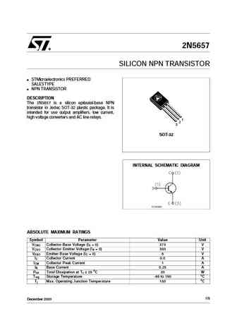
2N5657 SILICON NPN TRANSISTOR STMicroelectronics PREFERRED SALESTYPE NPN TRANSISTOR DESCRIPTION The 2N5657 is a silicon epitaxial-base NPN transistor in Jedec SOT-32 plastic package. It is intended for use output amplifiers, low current, high voltage converters and AC line relays. 1 2 3 SOT-32 INTERNAL SCHEMATIC DIAGRAM ABSOLUTE MAXIMUM RATINGS Symbol Parameter Value Un
2n5639.pdf
2N5639 N-Channel Switch This device is designed for low level analog switchng, sample and hold circuits and chopper stabilized amplifiers. Sourced from process 51. TO-92 1 1. Drain 2. Source 3. Gate Absolute Maximum Ratings * TC=25 C unless otherwise noted Symbol Parameter Value Units VDG Drain-Gate Voltage 30 V VGS Gate-Source Voltage -30 V IGF Forward Gate Current 50 mA
2n5638.pdf

2N5638 N-Channel Switch This device is designed for low level analog switchng, sample and hold circuits and chopper stabilized amplifiers. Sourced from process 51. TO-92 1 1. Drain 2. Source 3. Gate Absolute Maximum Ratings * TC=25 C unless otherwise noted Symbol Parameter Value Units VDG Drain-Gate Voltage 30 V VGS Gate-Source Voltage -30 V IGF Forward Gate Current 50 mA
2n5679 2n5680 2n5681 2n5682.pdf
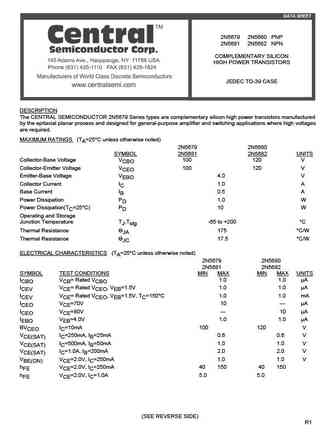
DATA SHEET 2N5679 2N5680 PNP 2N5681 2N5682 NPN COMPLEMENTARY SILICON HIGH POWER TRANSISTORS JEDEC TO-39 CASE DESCRIPTION The CENTRAL SEMICONDUCTOR 2N5679 Series types are complementary silicon high power transistors manufactured by the epitaxial planar process and designed for general-purpose amplifier and switching applications where high voltages are required. MAXIMUM RATIN
2n5629 2n5630 2n6029 2n6030.pdf
145 Adams Avenue, Hauppauge, NY 11788 USA Tel (631) 435-1110 Fax (631) 435-1824
2n5655g.pdf
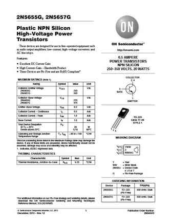
2N5655G, 2N5657G Plastic NPN Silicon High-Voltage Power Transistors These devices are designed for use in line-operated equipment such as audio output amplifiers; low-current, high-voltage converters; and http //onsemi.com AC line relays. 0.5 AMPERE Features POWER TRANSISTORS Excellent DC Current Gain NPN SILICON High Current-Gain - Bandwidth Product 250-350 VOLTS, 20 WATT
2n5684 2n5686.pdf

2N5684 (PNP), 2N5686 (NPN) High-Current Complementary Silicon Power Transistors These packages are designed for use in high-power amplifier and switching circuit applications. http //onsemi.com Features 50 AMPERE High Current Capability - IC Continuous = 50 Amperes COMPLEMENTARY SILICON DC Current Gain - hFE = 15 - 60 @ IC = 25 Adc POWER TRANSISTORS Low Collector-Emitte
2n5638 2n5639.pdf
2N5638, 2N5639 2N5638 is a Preferred Device JFET Chopper Transistors N-Channel - Depletion N-Channel Junction Field Effect Transistors, depletion mode (Type A) designed for chopper and high-speed switching applications. Features http //onsemi.com Low Drain-Source ON Resistance RDS(on) = 30W for 2N5638 RDS(on) = 60W for 2N5639 1 DRAIN Low Reverse Transfer Capacitance -
2n5655 2n5657.pdf
2N5655, 2N5657 Plastic NPN Silicon High-Voltage Power Transistor These devices are designed for use in line-operated equipment such as audio output amplifiers; low-current, high-voltage converters; and http //onsemi.com AC line relays. 0.5 AMPERE Features POWER TRANSISTORS Excellent DC Current Gain - NPN SILICON hFE = 30-250 @ IC = 100 mAdc 250-350 VOLTS, 20 WATTS Current
2n5657g.pdf

2N5655, 2N5657 Plastic NPN Silicon High-Voltage Power Transistor These devices are designed for use in line-operated equipment such as audio output amplifiers; low-current, high-voltage converters; and http //onsemi.com AC line relays. 0.5 AMPERE Features POWER TRANSISTORS Excellent DC Current Gain - NPN SILICON hFE = 30-250 @ IC = 100 mAdc 250-350 VOLTS, 20 WATTS Current
2n5655g 2n5657g.pdf

2N5655G, 2N5657G Plastic NPN Silicon High-Voltage Power Transistors These devices are designed for use in line-operated equipment such as audio output amplifiers; low-current, high-voltage converters; and http //onsemi.com AC line relays. 0.5 AMPERE Features POWER TRANSISTORS Excellent DC Current Gain NPN SILICON High Current-Gain - Bandwidth Product 250-350 VOLTS, 20 WATT
2n5631-d.pdf
2N5631 High-Voltage - High Power Transistors High-voltage - high power transistors designed for use in high power audio amplifier applications and high voltage switching regulator circuits. http //onsemi.com High Collector Emitter Sustaining Voltage - VCEO(sus) = 140 Vdc 16 AMPERE High DC Current Gain - @ IC = 8.0 Adc hFE = 15 (Min) POWER TRANSISTORS Low Collector-Emitt
2n5684g.pdf

2N5684 (PNP), 2N5686 (NPN) High-Current Complementary Silicon Power Transistors These packages are designed for use in high-power amplifier and switching circuit applications. http //onsemi.com Features 50 AMPERE High Current Capability - IC Continuous = 50 Amperes COMPLEMENTARY SILICON DC Current Gain - hFE = 15 - 60 @ IC = 25 Adc POWER TRANSISTORS Low Collector-Emitte
2n5686g.pdf
2N5684 (PNP), 2N5686 (NPN) High-Current Complementary Silicon Power Transistors These packages are designed for use in high-power amplifier and switching circuit applications. http //onsemi.com Features 50 AMPERE High Current Capability - IC Continuous = 50 Amperes COMPLEMENTARY SILICON DC Current Gain - hFE = 15 - 60 @ IC = 25 Adc POWER TRANSISTORS Low Collector-Emitte
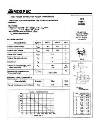
2n5671-2n5672.pdf
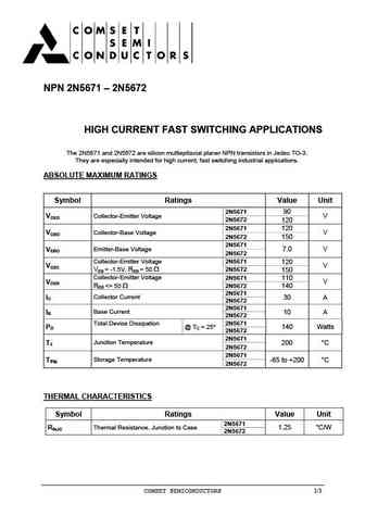
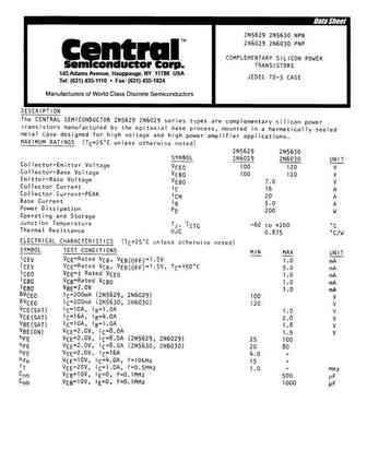
NPN 2N5671 2N5672 HIGH CURRENT FAST SWITCHING APPLICATIONS HIGH CURRENT FAST SWITCHING APPLICATIONS The 2N5671 and 2N5672 are silicon multiepitaxial planer NPN transistors in Jedec TO-3. They are especially intended for high current, fast switching industrial applications. ABSOLUTE MAXIMUM RATINGS Symbol Ratings Value Unit 2N5671 90 VCEO Collector-Emitter Voltage V 2N5672 120 2N56
2n5609.pdf
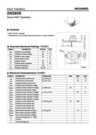
Power Transistors INCHANGE 2N5609 Silicon PNP Transistors Features With TO-66 package Designed for use as high-frequency drivers in audio amplifier Absolute Maximum Ratings Tc=25 SYMBOL PARAMETER RATING UNIT VCBO Collector to base voltage 80 V VCEO Collector to emitter voltage 80 V VEBO Emitter to base voltage 5.0 V ICP Peak collector current A IC Collector current 5.0 A PC
2n5632.pdf
2N5632 Dimensions in mm (inches). Bipolar NPN Device in a Hermetically sealed TO3 25.15 (0.99) 6.35 (0.25) 26.67 (1.05) 9.15 (0.36) Metal Package. 10.67 (0.42) 11.18 (0.44) 1.52 (0.06) 3.43 (0.135) 1 2 Bipolar NPN Device. 3 VCEO = 100V (case) 3.84 (0.151) 4.09 (0.161) 7.92 (0.312) IC = 10A 12.70 (0.50) All Semelab hermetically sealed products can be processed in
2n5620.pdf

2N5620 Dimensions in mm (inches). Bipolar NPN Device in a Hermetically sealed TO3 25.15 (0.99) 6.35 (0.25) 26.67 (1.05) 9.15 (0.36) Metal Package. 10.67 (0.42) 11.18 (0.44) 1.52 (0.06) 3.43 (0.135) 1 2 Bipolar NPN Device. 3 VCEO = 100V (case) 3.84 (0.151) 4.09 (0.161) 7.92 (0.312) IC = 5A 12.70 (0.50) All Semelab hermetically sealed products can be processed in a
2n5665n1.pdf
NPN POWER SILICON SWITCHING TRANSISTOR 2N5665N1 Hermetic SMD0.5 Ceramic Surface Mount. Ideally Suited for Power Amplifier and Switching Applications. Screening Options Available ABSOLUTE MAXIMUM RATINGS (TC = 25 C unless otherwise stated) VCBO Collector Base Voltage 400V VCEO Collector Emitter Voltage 300V VEBO Emitter Base Voltage 6V IC Cont
2n5675.pdf
2N5675 Dimensions in mm (inches). Bipolar PNP Device in a 8.51 (0.34) 9.40 (0.37) Hermetically sealed TO39 7.75 (0.305) 8.51 (0.335) Metal Package. 6.10 (0.240) 6.60 (0.260) Bipolar PNP Device. 0.89 max. (0.035) 12.70 (0.500) min. 0.41 (0.016) 0.53 (0.021) VCEO = 100V dia. IC = 2A 5.08 (0.200) typ. 2.54 All Semelab hermetically sealed products 2 (0.100) 1 3
2n5667n1.pdf
NPN POWER SILICON SWITCHING TRANSISTOR 2N5667N1 Hermetic SMD0.5 Ceramic Surface Mount. Ideally Suited for Power Amplifier and Switching Applications. Screening Options Available ABSOLUTE MAXIMUM RATINGS (TC = 25 C unless otherwise stated) VCBO Collector Base Voltage 400V VCEO Collector Emitter Voltage 300V VEBO Emitter Base Voltage 6V IC Cont
2n5601.pdf
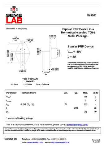
2N5601 Dimensions in mm (inches). Bipolar PNP Device in a Hermetically sealed TO66 6.35 (0.250) Metal Package. 8.64 (0.340) 3.68 (0.145) rad. 3.61 (0.142) max. 4.08(0.161) rad. Bipolar PNP Device. 1 2 VCEO = 80V IC = 2A All Semelab hermetically sealed products can be processed in accordance with the requirements of BS, CECC and JAN, JANTX, JANTXV and JANS specif
2n5608.pdf
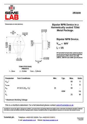
2N5608 Dimensions in mm (inches). Bipolar NPN Device in a Hermetically sealed TO66 6.35 (0.250) Metal Package. 8.64 (0.340) 3.68 (0.145) rad. 3.61 (0.142) max. 4.08(0.161) rad. Bipolar NPN Device. 1 2 VCEO = 80V IC = 5A All Semelab hermetically sealed products can be processed in accordance with the requirements of BS, CECC and JAN, JANTX, JANTXV and JANS specif
2n5603.pdf
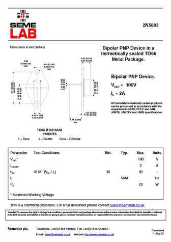
2N5603 Dimensions in mm (inches). Bipolar PNP Device in a Hermetically sealed TO66 6.35 (0.250) Metal Package. 8.64 (0.340) 3.68 (0.145) rad. 3.61 (0.142) max. 4.08(0.161) rad. Bipolar PNP Device. 1 2 VCEO = 100V IC = 2A All Semelab hermetically sealed products can be processed in accordance with the requirements of BS, CECC and JAN, JANTX, JANTXV and JANS speci
2n5606.pdf
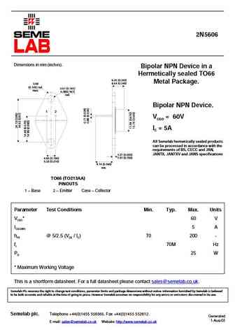
2N5606 Dimensions in mm (inches). Bipolar NPN Device in a Hermetically sealed TO66 6.35 (0.250) Metal Package. 8.64 (0.340) 3.68 (0.145) rad. 3.61 (0.142) max. 4.08(0.161) rad. Bipolar NPN Device. 1 2 VCEO = 60V IC = 5A All Semelab hermetically sealed products can be processed in accordance with the requirements of BS, CECC and JAN, JANTX, JANTXV and JANS specif
2n5623.pdf

2N5623 Dimensions in mm (inches). Bipolar PNP Device in a Hermetically sealed TO3 25.15 (0.99) 6.35 (0.25) 26.67 (1.05) 9.15 (0.36) Metal Package. 10.67 (0.42) 11.18 (0.44) 1.52 (0.06) 3.43 (0.135) 1 2 Bipolar PNP Device. 3 VCEO = 80V (case) 3.84 (0.151) 4.09 (0.161) 7.92 (0.312) IC = 10A 12.70 (0.50) All Semelab hermetically sealed products can be processed in a
2n5613.pdf
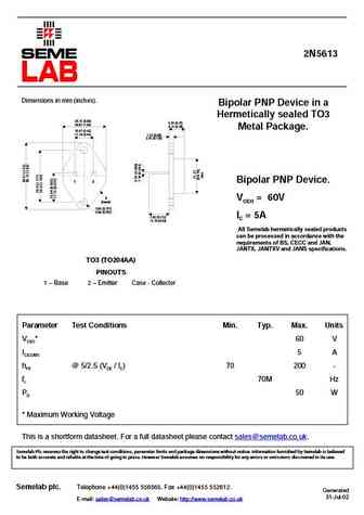
2N5613 Dimensions in mm (inches). Bipolar PNP Device in a Hermetically sealed TO3 25.15 (0.99) 6.35 (0.25) 26.67 (1.05) 9.15 (0.36) Metal Package. 10.67 (0.42) 11.18 (0.44) 1.52 (0.06) 3.43 (0.135) 1 2 Bipolar PNP Device. 3 VCEO = 60V (case) 3.84 (0.151) 4.09 (0.161) 7.92 (0.312) IC = 5A 12.70 (0.50) All Semelab hermetically sealed products can be processed in ac
2n5619.pdf

2N5619 Dimensions in mm (inches). Bipolar PNP Device in a Hermetically sealed TO3 25.15 (0.99) 6.35 (0.25) 26.67 (1.05) 9.15 (0.36) Metal Package. 10.67 (0.42) 11.18 (0.44) 1.52 (0.06) 3.43 (0.135) 1 2 Bipolar PNP Device. 3 VCEO = 80V (case) 3.84 (0.151) 4.09 (0.161) 7.92 (0.312) IC = 5A 12.70 (0.50) All Semelab hermetically sealed products can be processed in ac
2n5665smd.pdf
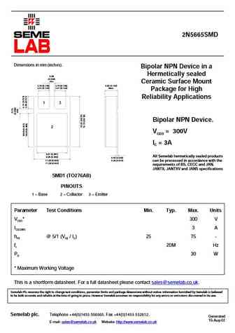
2N5665SMD Dimensions in mm (inches). Bipolar NPN Device in a Hermetically sealed 0.89 (0.035) min. Ceramic Surface Mount 3.70 (0.146) 3.70 (0.146) 3.60 (0.142) 3.41 (0.134) 3.41 (0.134) Max. Package for High Reliability Applications 1 3 Bipolar NPN Device. 2 VCEO = 300V IC = 3A 9.67 (0.381) All Semelab hermetically sealed products 9.38 (0.369) 0.50 (0.020) 0.26 (
2n5605.pdf

2N5605 Dimensions in mm (inches). Bipolar PNP Device in a Hermetically sealed TO66 6.35 (0.250) Metal Package. 8.64 (0.340) 3.68 (0.145) rad. 3.61 (0.142) max. 4.08(0.161) rad. Bipolar PNP Device. 1 2 VCEO = 60V IC = 5A All Semelab hermetically sealed products can be processed in accordance with the requirements of BS, CECC and JAN, JANTX, JANTXV and JANS specif
2n5633.pdf

2N5633 Dimensions in mm (inches). Bipolar NPN Device in a Hermetically sealed TO3 25.15 (0.99) 6.35 (0.25) 26.67 (1.05) 9.15 (0.36) Metal Package. 10.67 (0.42) 11.18 (0.44) 1.52 (0.06) 3.43 (0.135) 1 2 Bipolar NPN Device. 3 VCEO = 80V (case) 3.84 (0.151) 4.09 (0.161) 7.92 (0.312) IC = 10A 12.70 (0.50) All Semelab hermetically sealed products can be processed in a
2n5664smd05.pdf
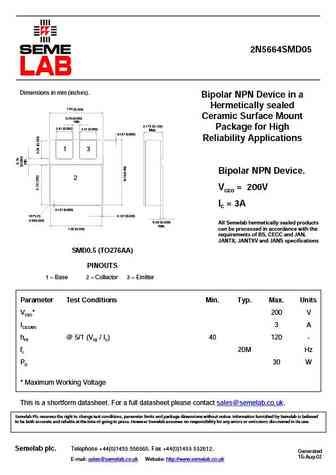
2N5664SMD05 Dimensions in mm (inches). Bipolar NPN Device in a Hermetically sealed 7.54 (0.296) 0.76 (0.030) Ceramic Surface Mount min. 3.175 (0.125) 2.41 (0.095) Package for High 2.41 (0.095) Max. 0.127 (0.005) Reliability Applications 1 3 Bipolar NPN Device. 2 VCEO = 200V IC = 3A 0.127 (0.005) 16 PLCS 0.127 (0.005) 0.50(0.020) 0.50 (0.020) All Semelab her
2n5617.pdf

2N5617 Dimensions in mm (inches). Bipolar PNP Device in a Hermetically sealed TO3 25.15 (0.99) 6.35 (0.25) 26.67 (1.05) 9.15 (0.36) Metal Package. 10.67 (0.42) 11.18 (0.44) 1.52 (0.06) 3.43 (0.135) 1 2 Bipolar PNP Device. 3 VCEO = 80V (case) 3.84 (0.151) 4.09 (0.161) 7.92 (0.312) IC = 5A 12.70 (0.50) All Semelab hermetically sealed products can be processed in ac
2n5681smd05.pdf

2N5681SMD05 Dimensions in mm (inches). Bipolar NPN Device in a Hermetically sealed 7.54 (0.296) 0.76 (0.030) Ceramic Surface Mount min. 3.175 (0.125) 2.41 (0.095) Package for High 2.41 (0.095) Max. 0.127 (0.005) Reliability Applications 1 3 Bipolar NPN Device. 2 VCEO = 100V IC = 1A 0.127 (0.005) 16 PLCS 0.127 (0.005) 0.50(0.020) 0.50 (0.020) All Semelab her
2n5600.pdf

2N5600 Dimensions in mm (inches). Bipolar PNP Device in a Hermetically sealed TO66 6.35 (0.250) Metal Package. 8.64 (0.340) 3.68 (0.145) rad. 3.61 (0.142) max. 4.08(0.161) rad. Bipolar PNP Device. 1 2 VCEO = 80V IC = 2A All Semelab hermetically sealed products can be processed in accordance with the requirements of BS, CECC and JAN, JANTX, JANTXV and JANS specif
2n5666smd05.pdf

2N5666SMD05 Dimensions in mm (inches). Bipolar NPN Device in a Hermetically sealed 7.54 (0.296) 0.76 (0.030) Ceramic Surface Mount min. 3.175 (0.125) 2.41 (0.095) Package for High 2.41 (0.095) Max. 0.127 (0.005) Reliability Applications 1 3 Bipolar NPN Device. 2 VCEO = 200V IC = 3A 0.127 (0.005) 16 PLCS 0.127 (0.005) 0.50(0.020) 0.50 (0.020) All Semelab her
2n5622.pdf
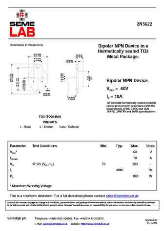
2N5622 Dimensions in mm (inches). Bipolar NPN Device in a Hermetically sealed TO3 25.15 (0.99) 6.35 (0.25) 26.67 (1.05) 9.15 (0.36) Metal Package. 10.67 (0.42) 11.18 (0.44) 1.52 (0.06) 3.43 (0.135) 1 2 Bipolar NPN Device. 3 VCEO = 60V (case) 3.84 (0.151) 4.09 (0.161) 7.92 (0.312) IC = 10A 12.70 (0.50) All Semelab hermetically sealed products can be processed in a
2n5634.pdf

2N5634 Dimensions in mm (inches). Bipolar NPN Device in a Hermetically sealed TO3 25.15 (0.99) 6.35 (0.25) 26.67 (1.05) 9.15 (0.36) Metal Package. 10.67 (0.42) 11.18 (0.44) 1.52 (0.06) 3.43 (0.135) 1 2 Bipolar NPN Device. 3 VCEO = 140V (case) 3.84 (0.151) 4.09 (0.161) 7.92 (0.312) IC = 10A 12.70 (0.50) All Semelab hermetically sealed products can be processed in
2n5666smd.pdf

2N5666SMD Dimensions in mm (inches). Bipolar NPN Device in a Hermetically sealed 0.89 (0.035) min. Ceramic Surface Mount 3.70 (0.146) 3.70 (0.146) 3.60 (0.142) 3.41 (0.134) 3.41 (0.134) Max. Package for High Reliability Applications 1 3 Bipolar NPN Device. 2 VCEO = 200V IC = 3A 9.67 (0.381) All Semelab hermetically sealed products 9.38 (0.369) 0.50 (0.020) 0.26 (
2n5611.pdf

2N5611 Dimensions in mm (inches). Bipolar PNP Device in a Hermetically sealed TO66 6.35 (0.250) Metal Package. 8.64 (0.340) 3.68 (0.145) rad. 3.61 (0.142) max. 4.08(0.161) rad. Bipolar PNP Device. 1 2 VCEO = 100V IC = 5A All Semelab hermetically sealed products can be processed in accordance with the requirements of BS, CECC and JAN, JANTX, JANTXV and JANS speci
2n5664smd.pdf
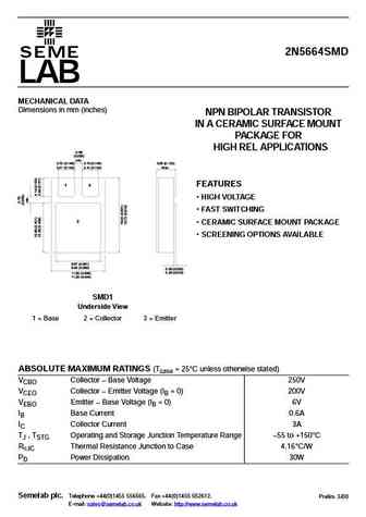
2N5664SMD SEME LAB MECHANICAL DATA Dimensions in mm (inches) NPN BIPOLAR TRANSISTOR IN A CERAMIC SURFACE MOUNT PACKAGE FOR HIGH REL APPLICATIONS FEATURES ! HIGH VOLTAGE FAST SWITCHING CERAMIC SURFACE MOUNT PACKAGE SCREENING OPTIONS AVAILABLE
2n5643.pdf
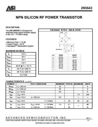
2N5643 NPN SILICON RF POWER TRANSISTOR DESCRIPTION PACKAGE STYLE .380 4L STUD The ASI 2N5643 is Designed for .112x45 A wideband large-signal amplifier stages in the 125 175 MHz range. C B E E FEATURES C B Minimum Gain = 7.6 dB Output Power = 40 W I D H Omnigold Metalization System J G #8-32 UNC-2A F MAXIMUM RATINGS E IC 5.0
2n5679 2n5680 2n5681 2n5682.pdf
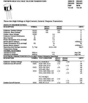
IS/ISO 9002 IS / IECQC 700000 Lic# QSC/L- 000019.2 IS / IECQC 750100 Continental Device India Limited An IS/ISO 9002 and IECQ Certified Manufacturer PNP/NPN HIGH VOLTAGE SILICON TRANSISTORS 2N5679 2N5681 2N5680 2N5682 PNP NPN TO-39 TO-39 Boca Semiconductor Corp. BSC These Are High Voltage & High Current, General Purpose Transistors ABSOLUTE MAXIMUM RATINGS. DESCRIPTION SYMBOL 2N5
2n5679 2n5680 81 82.pdf
Continental Device India Limited An ISO/TS 16949, ISO 9001 and ISO 14001 Certified Company PNP/NPN HIGH VOLTAGE SILICON TRANSISTORS 2N5679 2N5681 2N5680 2N5682 PNP NPN TO-39 TO-39 These Are High Voltage & High Current, General Purpose Transistors ABSOLUTE MAXIMUM RATINGS. DESCRIPTION SYMBOL 2N5679 2N5680 UNITS 2N5681 2N5682 Collector -Emitter Voltage VCEO 100 120 V Collector -Base
2n5622 2n5624 2n5626 2n5628.pdf
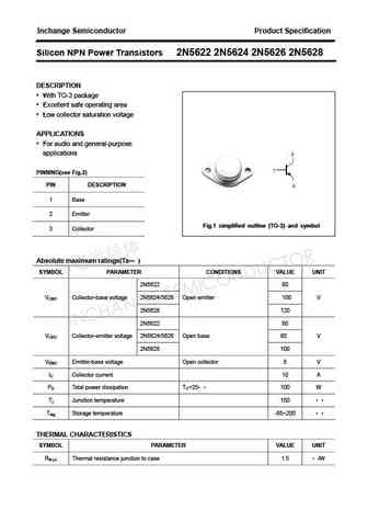
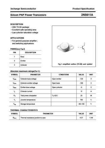
Product Specification www.jmnic.com Silicon NPN Power Transistors 2N5622 2N5624 2N5626 2N5628 DESCRIPTION With TO-3 package Excellent safe operating area Low collector-emitter saturation voltage APPLICATIONS For audio and general-purpose applications PINNING(see Fig.2) PIN DESCRIPTION 1 Base 2 Emitter 3 Collector Fig.1 simplified outline (TO-3) and symbol Abso
2n5629 2n5630.pdf
Product Specification www.jmnic.com Silicon NPN Power Transistors 2N5629 2N5630 DESCRIPTION With TO-3 package Complement to type 2N6029 2N6030 APPLICATIONS For high voltage and high power amplifier applications PINNING PIN DESCRIPTION 1 Base 2 Emitter 3 Collector Fig.1 simplified outline (TO-3) and symbol Absolute maximum ratings(Ta= ) SYMBOL PARAMETER CONDITIO
2n5606 2n5608 2n5610 2n5612.pdf
Product Specification www.jmnic.com Silicon NPN Power Transistors 2N5606 2N5608 2N5610 2N5612 DESCRIPTION With TO-66 package Excellent safe operating area Low collector-emitter saturation voltage APPLICATIONS For general-purpose amplifier ; and switching applications PINNING(see Fig.2) PIN DESCRIPTION 1 Base 2 Emitter 3 Collector Fig.1 simplified outline (TO-66)
2n5631.pdf
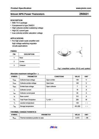
Product Specification www.jmnic.com Silicon NPN Power Transistors 2N5631 DESCRIPTION With TO-3 package Complement to type 2N6031 High collector-emitter sustaining voltage High DC current gain Low collector-emitter saturation voltage APPLICATIONS For high power audio amplifier and high voltage switching regulator circuits applications PINNING PIN DESCRIPTION
2n5621 2n5623 2n5625 2n5627.pdf
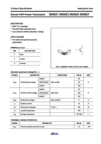
Product Specification www.jmnic.com Silicon PNP Power Transistors 2N5621 2N5623 2N5625 2N5627 DESCRIPTION With TO-3 package Excellent safe operating area Low collector-emitter saturation voltage APPLICATIONS For audio and general-purpose applications PINNING(see Fig.2) PIN DESCRIPTION 1 Base 2 Emitter 3 Collector Fig.1 simplified outline (TO-3) and symbol Abso
2n5598 2n5600 2n5602 2n5604.pdf
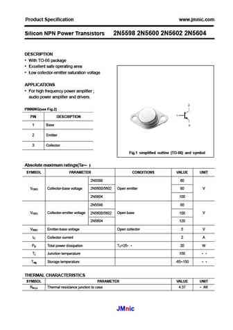
Product Specification www.jmnic.com Silicon NPN Power Transistors 2N5598 2N5600 2N5602 2N5604 DESCRIPTION With TO-66 package Excellent safe operating area Low collector-emitter saturation voltage APPLICATIONS For high frequency power amplifier ; audio power amplifier and drivers. PINNING(see Fig.2) PIN DESCRIPTION 1 Base 2 Emitter 3 Collector Fig.1 simplified ou
2n5605 2n5607 2n5609 2n5611.pdf
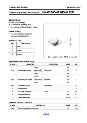
Product Specification www.jmnic.com Silicon PNP Power Transistors 2N5605 2N5607 2N5609 2N5611 DESCRIPTION With TO-66 package Excellent safe operating area Low collector-emitter saturation voltage APPLICATIONS For general-purpose amplifier ; and switching applications PINNING(see Fig.2) PIN DESCRIPTION 1 Base 2 Emitter 3 Collector Fig.1 simplified outline (TO-66)
2n5597 2n5599 2n5601 2n5603.pdf

Product Specification www.jmnic.com Silicon PNP Power Transistors 2N5597 2N5599 2N5601 2N5603 DESCRIPTION With TO-66 package Excellent safe operating area Low collector-emitter saturation voltage APPLICATIONS For high frequency power amplifier ; audio power amplifier and drivers. PINNING(see Fig.2) PIN DESCRIPTION 1 Base 2 Emitter 3 Collector Fig.1 simplified ou
2n5655 2n5656 2n5657.pdf
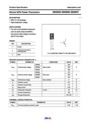
Product Specification www.jmnic.com Silicon NPN Power Transistors 2N5655 2N5656 2N5657 DESCRIPTION With TO-126 package High breakdown voltage APPLICATIONS For use in line-operated equipment such as audio output amplifiers; low-current ,high-voltage converters; and AC line relays PINNING PIN DESCRIPTION 1 Emitter Collector;connected to 2 mounting base 3 Bas
2n5632 2n5633 2n5634.pdf
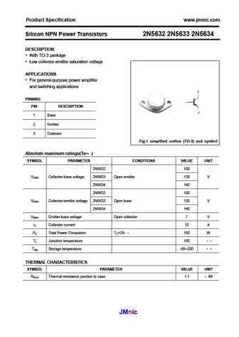
Product Specification www.jmnic.com Silicon NPN Power Transistors 2N5632 2N5633 2N5634 DESCRIPTION With TO-3 package Low collector-emitter saturation voltage APPLICATIONS For general-purpose power amplifier and switching applications PINNING PIN DESCRIPTION 1 Base 2 Emitter 3 Collector Fig.1 simplified outline (TO-3) and symbol Absolute maximum ratings(Ta= ) SY
2n5666u3.pdf

TECHNICAL DATA SHEET 6 Lake Street, Lawrence, MA 01841 1-800-446-1158 / (978) 620-2600 / Fax (978) 689-0803 Website http //www.microsemi.com NPN POWER SILICON SWITCHING TRANSISTOR Qualified per MIL-PRF-19500/455 DEVICES LEVELS 2N5664 2N5666 2N5667 JAN 2N5665 2N5666S 2N5667S JANTX 2N5666U3 JANTV JANS ABSOLUTE MAXIMUM RATINGS (TC = +25 C unless otherwise noted) 2N5664 2N5
2n5666s.pdf

TECHNICAL DATA SHEET 6 Lake Street, Lawrence, MA 01841 1-800-446-1158 / (978) 620-2600 / Fax (978) 689-0803 Website http //www.microsemi.com NPN POWER SILICON SWITCHING TRANSISTOR Qualified per MIL-PRF-19500/455 DEVICES LEVELS 2N5664 2N5666 2N5667 JAN 2N5665 2N5666S 2N5667S JANTX 2N5666U3 JANTV JANS ABSOLUTE MAXIMUM RATINGS (TC = +25 C unless otherwise noted) 2N5664 2N5
2n5661u3.pdf

TECHNICAL DATA SHEET 6 Lake Street, Lawrence, MA 01841 Gort Road Business Park, Ennis, Co. Clare, Ireland 1-800-446-1158 / (978) 620-2600 / Fax (978) 689-0803 Tel +353 (0) 65 6840044 Fax +353 (0) 65 6822298 Website http //www.microsemi.com NPN POWER SILICON TRANSISTOR Qualified per MIL-PRF-19500/454 DEVICES LEVELS 2N5660 2N5661 2N5662 JAN 2N5660U3 2N5661U3 2N5663 JANTX JANT
2n5660 2n5661 2n5662 2n5663.pdf
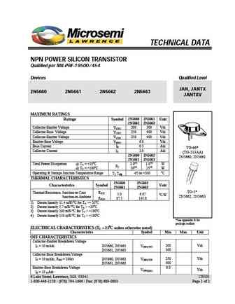
TECHNICAL DATA NPN POWER SILICON TRANSISTOR Qualified per MIL-PRF-19500/454 Devices Qualified Level JAN, JANTX 2N5660 2N5661 2N5662 2N5663 JANTXV MAXIMUM RATINGS 2N5660 2N5661 Ratings Symbol Unit 2N5662 2N5663 Collector-Emitter Voltage 200 300 Vdc VCEO Collector-Base Voltage 250 400 Vdc VCBO Collector-Emitter Voltage 250 400 Vdc VCER Emitter-Base Voltage 6.0
2n5667s.pdf
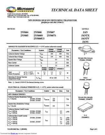
TECHNICAL DATA SHEET 6 Lake Street, Lawrence, MA 01841 1-800-446-1158 / (978) 620-2600 / Fax (978) 689-0803 Website http //www.microsemi.com NPN POWER SILICON SWITCHING TRANSISTOR Qualified per MIL-PRF-19500/455 DEVICES LEVELS 2N5664 2N5666 2N5667 JAN 2N5665 2N5666S 2N5667S JANTX 2N5666U3 JANTV JANS ABSOLUTE MAXIMUM RATINGS (TC = +25 C unless otherwise noted) 2N5664 2N5
2n5664-65-66-67.pdf
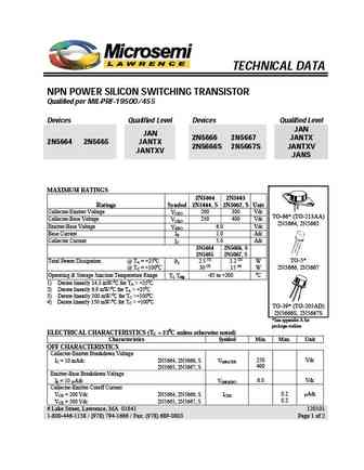
TECHNICAL DATA NPN POWER SILICON SWITCHING TRANSISTOR Qualified per MIL-PRF-19500/455 Devices Qualified Level Devices Qualified Level JAN JAN 2N5666 2N5667 JANTX 2N5664 2N5665 JANTX 2N5666S 2N5667S JANTXV JANTXV JANS MAXIMUM RATINGS 2N5664 2N5665 Ratings Symbol 2N5666, S 2N5667, S Unit Collector-Emitter Voltage 200 300 Vdc VCEO TO-66* (TO-213AA) Collector-Ba
2n5660u3.pdf
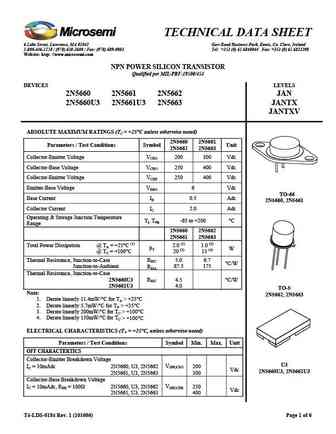
TECHNICAL DATA SHEET 6 Lake Street, Lawrence, MA 01841 Gort Road Business Park, Ennis, Co. Clare, Ireland 1-800-446-1158 / (978) 620-2600 / Fax (978) 689-0803 Tel +353 (0) 65 6840044 Fax +353 (0) 65 6822298 Website http //www.microsemi.com NPN POWER SILICON TRANSISTOR Qualified per MIL-PRF-19500/454 DEVICES LEVELS 2N5660 2N5661 2N5662 JAN 2N5660U3 2N5661U3 2N5663 JANTX JANT
2n5679 2n5680.pdf
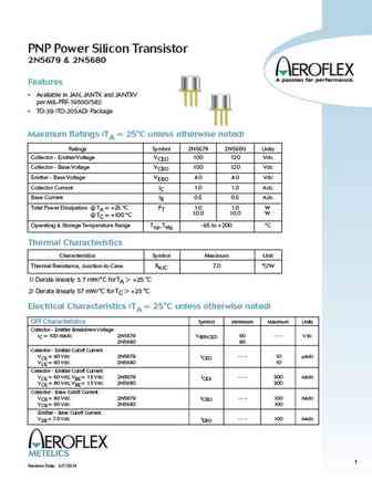
PNP Power Silicon Transistor 2N5679 & 2N5680 Features Available in JAN, JANTX and JANTXV per MIL-PRF-19500/582 TO-39 (TO-205AD) Package Maximum Ratings (TA = 25 C unless otherwise noted) Ratings Symbol 2N5679 2N5680 Units Collector - Emitter Voltage VCEO 100 120 Vdc Collector - Base Voltage VCBO 100 120 Vdc Emitter - Base Voltage VEBO 4.0 4.0 Vdc Collector Current IC 1.0 1.0
2n5672.pdf
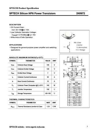
SPTECH Product Specification SPTECH Silicon NPN Power Transistors 2N5672 DESCRIPTION DC Current Gain- h = 20 100@I = 15A FE C Low Collector Saturation Voltage- V )= 0.75V(Max)@ I = 15A CE(sat C Wide Area of Safe Operation APPLICATIONS Designed for general purpose power amplifier and switching applications. ABSOLUTE MAXIMUM RATINGS(T =25 ) a SYMBOL PARAMETER VALUE UN
2n5631.pdf
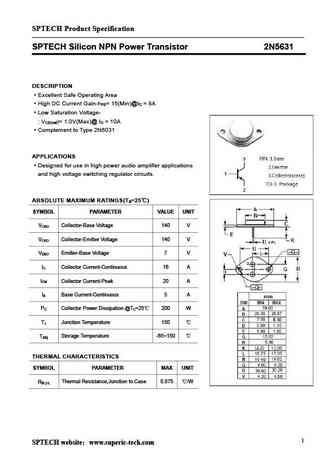
SPTECH Product Specification SPTECH Silicon NPN Power Transistor 2N5631 DESCRIPTION Excellent Safe Operating Area High DC Current Gain-h = 15(Min)@I = 8A FE C Low Saturation Voltage- V )= 1.0V(Max)@ I = 10A CE(sat C Complement to Type 2N6031 APPLICATIONS Designed for use in high power audio amplifier applications and high voltage switching regulator circuits. ABSOLUTE M
2n5622 2n5624 2n5626 2n5628.pdf
Inchange Semiconductor Product Specification Silicon NPN Power Transistors 2N5622 2N5624 2N5626 2N5628 DESCRIPTION With TO-3 package Excellent safe operating area Low collector saturation voltage APPLICATIONS For audio and general-purpose applications PINNING(see Fig.2) PIN DESCRIPTION 1 Base 2 Emitter Fig.1 simplified outline (TO-3) and symbol 3 Collector Abso
2n5629 2n5630.pdf

Inchange Semiconductor Product Specification Silicon NPN Power Transistors 2N5629 2N5630 DESCRIPTION With TO-3 package Complement to type 2N6029 2N6030 APPLICATIONS For high voltage and high power amplifier applications PINNING PIN DESCRIPTION 1 Base 2 Emitter Fig.1 simplified outline (TO-3) and symbol 3 Collector Absolute maximum ratings(Ta= ) SYMBOL PARAMETE
2n5606 2n5608 2n5610 2n5612.pdf
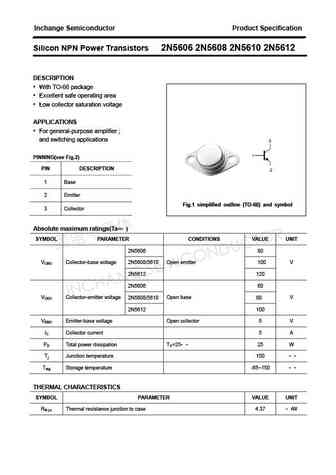
Inchange Semiconductor Product Specification Silicon NPN Power Transistors 2N5606 2N5608 2N5610 2N5612 DESCRIPTION With TO-66 package Excellent safe operating area Low collector saturation voltage APPLICATIONS For general-purpose amplifier ; and switching applications PINNING(see Fig.2) PIN DESCRIPTION 1 Base 2 Emitter Fig.1 simplified outline (TO-66) and symbol
2n5613 2n5615 2n5617 2n5619.pdf
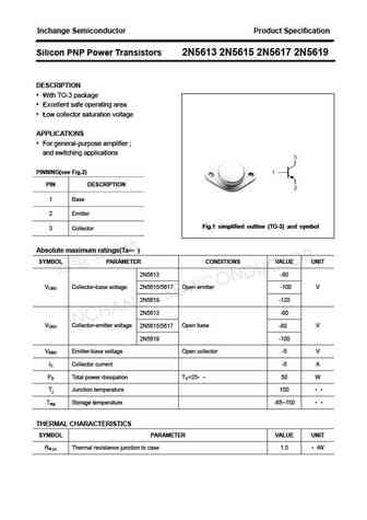
Inchange Semiconductor Product Specification Silicon PNP Power Transistors 2N5613 2N5615 2N5617 2N5619 DESCRIPTION With TO-3 package Excellent safe operating area Low collector saturation voltage APPLICATIONS For general-purpose amplifier ; and switching applications PINNING(see Fig.2) PIN DESCRIPTION 1 Base 2 Emitter Fig.1 simplified outline (TO-3) and symbol
2n5664 2n5665.pdf
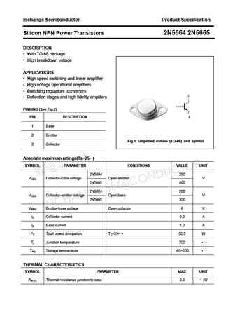
Inchange Semiconductor Product Specification Silicon NPN Power Transistors 2N5664 2N5665 DESCRIPTION With TO-66 package High breakdown voltage APPLICATIONS High speed switching and linear amplifier High-voltage operational amplifiers Switching regulators ,converters Deflection stages and high fidelity amplifers PINNING (See Fig.2) PIN DESCRIPTION 1 Base 2 Em
2n5631.pdf
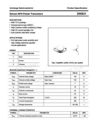
Inchange Semiconductor Product Specification Silicon NPN Power Transistors 2N5631 DESCRIPTION With TO-3 package Complement to type 2N6031 High collector-emitter sustaining voltage High DC current gain@IC=8A Low collector saturation voltage APPLICATIONS For high power audio amplifier and high voltage switching regulator circuits applications PINNING PIN DESC
2n5657.pdf
INCHANGE Semiconductor isc Product Specification isc Silicon NPN Power Transistors 2N5657 DESCRIPTION Collector-Emitter Sustaining Voltage- VCEO(SUS) = 350V(Min) DC Current Gain- hFE= 30-250@IC= 0.1A Low Saturation Voltage APPLICATIONS Designed for use in line-operated equipment such as audio output amplifiers; low-current, high-voltage converters; and AC
2n5621 2n5623 2n5625 2n5627.pdf
Inchange Semiconductor Product Specification Silicon PNP Power Transistors 2N5621 2N5623 2N5625 2N5627 DESCRIPTION With TO-3 package Excellent safe operating area Low collector saturation voltage APPLICATIONS For audio and general-purpose applications PINNING(see Fig.2) PIN DESCRIPTION 1 Base 2 Emitter Fig.1 simplified outline (TO-3) and symbol 3 Collector Abs
2n5671 2n5672.pdf
Inchange Semiconductor Product Specification Silicon NPN Power Transistors 2N5671 2N5672 DESCRIPTION With TO-3 package High current ,high speed APPLICATIONS Intended for high current and fast switching industrial applications PINNING PIN DESCRIPTION 1 Base 2 Emitter Fig.1 simplified outline (TO-3) and symbol 3 Collector Absolute maximum ratings(Ta= ) SYMBOL PA
2n5610.pdf
INCHANGE Semiconductor isc Product Specification isc Silicon NPN Power Transistors 2N5610 DESCRIPTION DC Current Gain- hFE= 70-200@IC= 2.5A Wide Area of Safe Operation Collector-Emitter Sustaining Voltage- VCEO(SUS)= 80V(Min) Complement to Type 2N5609 APPLICATIONS Designed for use in high frequency power amplifiers, audio power amplifier and drivers. ABSO
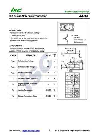
2n5665.pdf

isc Silicon NPN Power Transistor 2N5665 DESCRIPTION Collector-Emitter Breakdown Voltage- V =300V(Min) CEO Minimum Lot-to-Lot variations for robust device Performance and reliable operation APPLICATIONS Power amplifier and switching applications ABSOLUTE MAXIMUM RATINGS(Ta=25 ) UNI SYMBOL PARAMETER VALUE T V Collector-Base Voltage 400 V CBO V Collector-Emitter Voltage 30
2n5612a.pdf
Inchange Semiconductor Product Specification Silicon NPN Power Transistors 2N5612A DESCRIPTION With TO-66 package Excellent safe operating area Low collector saturation voltage APPLICATIONS For general-purpose amplifier ; and switching applications PINNING(see Fig.2) PIN DESCRIPTION 1 Base 2 Emitter Fig.1 simplified outline (TO-66) and symbol 3 Collector Absol
2n5598 2n5600 2n5602 2n5604.pdf
Inchange Semiconductor Product Specification Silicon NPN Power Transistors 2N5598 2N5600 2N5602 2N5604 DESCRIPTION With TO-66 package Excellent safe operating area Low collector saturation voltage APPLICATIONS For high frequency power amplifier ; audio power amplifier and drivers. PINNING(see Fig.2) PIN DESCRIPTION 1 Base 2 Emitter Fig.1 simplified outline (TO-66
2n5605 2n5607 2n5609 2n5611.pdf

Inchange Semiconductor Product Specification Silicon PNP Power Transistors 2N5605 2N5607 2N5609 2N5611 DESCRIPTION With TO-66 package Excellent safe operating area Low collector saturation voltage APPLICATIONS For general-purpose amplifier ; and switching applications PINNING(see Fig.2) PIN DESCRIPTION 1 Base 2 Emitter Fig.1 simplified outline (TO-66) and symbol
2n5619.pdf
INCHANGE Semiconductor isc Product Specification isc Silicon PNP Power Transistors 2N5619 DESCRIPTION DC Current Gain- hFE= 30-90@IC= -2.5A Wide Area of Safe Operation Collector-Emitter Sustaining Voltage- VCEO(SUS)= -100V(Min) Complement to Type 2N5620 APPLICATIONS Designed for use in high frequency power amplifiers, audio power amplifier and drivers. AB
2n5597 2n5599 2n5601 2n5603.pdf
Inchange Semiconductor Product Specification Silicon PNP Power Transistors 2N5597 2N5599 2N5601 2N5603 DESCRIPTION With TO-66 package Excellent safe operating area Low collector saturation voltage APPLICATIONS For high frequency power amplifier ; audio power amplifier and drivers. PINNING(see Fig.2) PIN DESCRIPTION 1 Base 2 Emitter Fig.1 simplified outline (TO-66
2n5611a.pdf
Inchange Semiconductor Product Specification Silicon PNP Power Transistors 2N5611A DESCRIPTION With TO-66 package Excellent safe operating area Low collector saturation voltage APPLICATIONS For general-purpose amplifier ; and switching applications PINNING(see Fig.2) PIN DESCRIPTION 1 Base 2 Emitter Fig.1 simplified outline (TO-66) and symbol 3 Collector Absolu
2n5660 2n5661.pdf

Inchange Semiconductor Product Specification Silicon NPN Power Transistors 2N5660 2N5661 DESCRIPTION With TO-66 package High breakdown voltage APPLICATIONS High speed switching and linear amplifier High-voltage operational amplifiers Switching regulators ,converters Deflection stages and high fidelity amplifers PINNING (See Fig.2) PIN DESCRIPTION 1 Base 2 Em
2n5614 2n5616 2n5618 2n5620.pdf
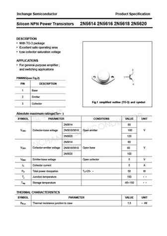
Inchange Semiconductor Product Specification Silicon NPN Power Transistors 2N5614 2N5616 2N5618 2N5620 DESCRIPTION With TO-3 package Excellent safe operating area Low collector saturation voltage APPLICATIONS For general-purpose amplifier ; and switching applications PINNING(see Fig.2) PIN DESCRIPTION 1 Base 2 Emitter Fig.1 simplified outline (TO-3) and symbol 3
2n5655 2n5656 2n5657.pdf
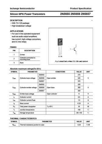
Inchange Semiconductor Product Specification Silicon NPN Power Transistors 2N5655 2N5656 2N5657 DESCRIPTION With TO-126 package High breakdown voltage APPLICATIONS For use in line-operated equipment such as audio output amplifiers; low-current ,high-voltage converters; and AC line relays PINNING PIN DESCRIPTION 1 Emitter Collector;connected to 2 mounting bas
2n5661.pdf
isc Silicon NPN Power Transistor 2N5661 DESCRIPTION Collector-Emitter Breakdown Voltage- V =300V(Min) CEO Minimum Lot-to-Lot variations for robust device Performance and reliable operation APPLICATIONS Power amplifier and switching applications ABSOLUTE MAXIMUM RATINGS(Ta=25 ) UNI SYMBOL PARAMETER VALUE T V Collector-Base Voltage 400 V CBO V Collector-Emitter Voltage 30
2n5632 2n5633 2n5634.pdf
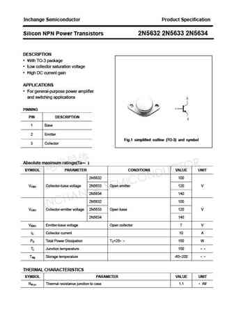
Inchange Semiconductor Product Specification Silicon NPN Power Transistors 2N5632 2N5633 2N5634 DESCRIPTION With TO-3 package Low collector saturation voltage High DC current gain APPLICATIONS For general-purpose power amplifier and switching applications PINNING PIN DESCRIPTION 1 Base 2 Emitter Fig.1 simplified outline (TO-3) and symbol 3 Collector Absolute m
2n5656.pdf
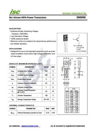
isc Silicon NPN Power Transistors 2N5656 DESCRIPTION Collector-Emitter Sustaining Voltage- V = 300V(Min) CEO(SUS) Low Saturation Voltage 100% avalanche tested Minimum Lot-to-Lot variations for robust device performance and reliable operation. APPLICATIONS Designed for use in line-operated equipment such as audio output amplifiers; low-current, high-voltage converters; and
2n5655.pdf
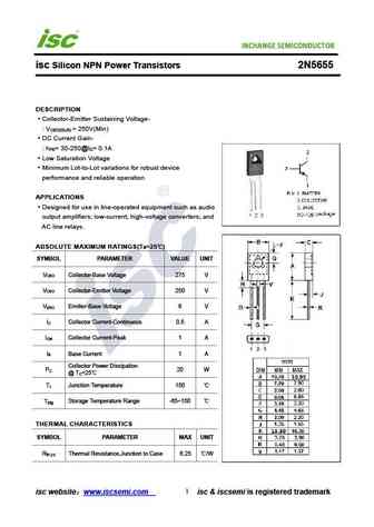
isc Silicon NPN Power Transistors 2N5655 DESCRIPTION Collector-Emitter Sustaining Voltage- V = 250V(Min) CEO(SUS) DC Current Gain- h = 30-250@I = 0.1A FE C Low Saturation Voltage Minimum Lot-to-Lot variations for robust device performance and reliable operation APPLICATIONS Designed for use in line-operated equipment such as audio output amplifiers; low-current, high-
2n5611.pdf
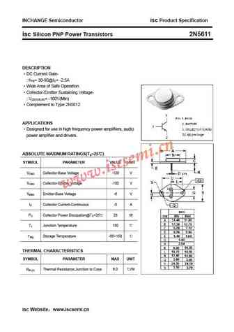
INCHANGE Semiconductor isc Product Specification isc Silicon PNP Power Transistors 2N5611 DESCRIPTION DC Current Gain- hFE= 30-90@IC= -2.5A Wide Area of Safe Operation Collector-Emitter Sustaining Voltage- VCEO(SUS)= -100V(Min) Complement to Type 2N5612 APPLICATIONS Designed for use in high frequency power amplifiers, audio power amplifier and drivers. ABS
2n5676.pdf
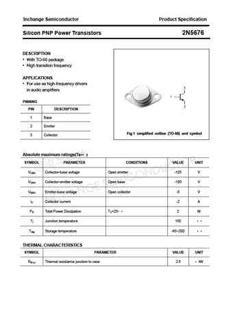
Inchange Semiconductor Product Specification Silicon PNP Power Transistors 2N5676 DESCRIPTION With TO-66 package High transition frequency APPLICATIONS For use as high-frequency drivers in audio amplifiers PINNING PIN DESCRIPTION 1 Base 2 Emitter Fig.1 simplified outline (TO-66) and symbol 3 Collector Absolute maximum ratings(Ta= ) SYMBOL PARAMETER CONDITIONS V
Другие транзисторы: 2N559, 2N5590, 2N5591, 2N5595, 2N5596, 2N5597, 2N5598, 2N5599, 2SC5200, 2N560, 2N5600, 2N5601, 2N5602, 2N5603, 2N5604, 2N5605, 2N5606
History: 2N1608 | 2N168 | 2N163A | 2N1864 | 2N1809 | ECH8502 | ED1702
🌐 : EN ES РУ

Список транзисторов
Обновления
BJT: GA1A4M | SBT42 | 2SA200-Y | 2SA200-O | 2SD882-Q | 2SD882-P | 2SD882-E | 2SC945-L | 2SC945-H | 2SC4226-R23 | 2SC3357-F | 2SC3357-E | 2SC3356-R26 | 2SC3356-R24 | 2SC3356-R23 | 2SB772-Q | 2SB772-P | 2SB772-E | 2SA1015-L | 2SA1015-H | HSS8550
Popular searches
mj21196g | irfb4115 | 21270 transistor | k3569 | irf640 datasheet | c945 transistor equivalent | irfz44 datasheet | tip3055 transistor