2N57. Аналоги и основные параметры
Наименование производителя: 2N57
Тип материала: Ge
Полярность: PNP
Предельные значения
Максимальная рассеиваемая мощность (Pc): 20 W
Макcимально допустимое напряжение коллектор-база (Ucb): 60 V
Макcимальный постоянный ток коллектора (Ic): 0.8 A
Предельная температура PN-перехода (Tj): 85 °C
Электрические характеристики
Граничная частота коэффициента передачи тока (ft): 0.2 MHz
Статический коэффициент передачи тока (hFE): 60
Корпус транзистора: TO3
Аналоги (замена) для 2N57
- подборⓘ биполярного транзистора по параметрам
2N57 даташит
2n5758re.pdf
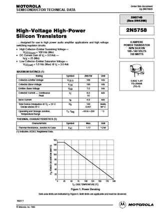
Order this document MOTOROLA by 2N5758/D SEMICONDUCTOR TECHNICAL DATA 2N5745 (See 2N4398) 2N5758 High-Voltage High-Power Silicon Transistors 6 AMPERE . . . designed for use in high power audio amplifier applications and high voltage POWER TRANSISTOR switching regulator circuits. NPN SILICON High Collector Emitter Sustaining Voltage 100 140 VOLTS VCEO(sus) = 100 Vdc (
2n5771 mmbt5771.pdf

2N5771 MMBT5771 C E C TO-92 B B SOT-23 E Mark 3R PNP Switching Transistor This device is designed for very high speed saturated switching at collector currents to 100 mA. Sourced from Process 65. See PN4258 for characteristics. Absolute Maximum Ratings* TA = 25 C unless otherwise noted Symbol Parameter Value Units VCEO Collector-Emitter Voltage 15 V VCBO Collector-Base Voltage
2n5771.pdf

2N5771 MMBT5771 C E C TO-92 B B SOT-23 E Mark 3R PNP Switching Transistor This device is designed for very high speed saturated switching at collector currents to 100 mA. Sourced from Process 65. See PN4258 for characteristics. Absolute Maximum Ratings* TA = 25 C unless otherwise noted Symbol Parameter Value Units VCEO Collector-Emitter Voltage 15 V VCBO Collector-Base Voltage
2n5772.pdf
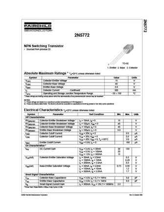
2N5772 NPN Switching Transistor Sourced from process 22. TO-92 1 1. Emitter 2. Base 3. Collector Absolute Maximum Ratings * Ta=25 C unless otherwise noted Symbol Parameter Value Units VCEO Collector-Emitter Voltage 15 V VCBO Collector-Base Voltage 40 V VEBO Emitter-Base Voltage 5.0 V IC Collector Current - Continued 300 mA TSTG Operating and Storage Junction Temperature Range -
2n5770.pdf
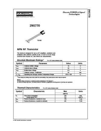
Discrete POWER & Signal Technologies 2N5770 C TO-92 B E NPN RF Transistor This device is designed for use as RF amplifiers, oscillators and multipliers with collector currents in the 1.0 mA to 30 mA range. Sourced from Process 43. See PN918 for characteristics. Absolute Maximum Ratings* TA = 25 C unless otherwise noted Symbol Parameter Value Units VCEO Collector-Emitter Voltage 15
2n5769.pdf
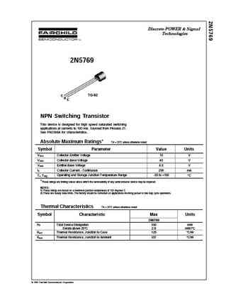
Discrete POWER & Signal Technologies 2N5769 C TO-92 B E NPN Switching Transistor This device is designed for high speed saturated switching applications at currents to 100 mA. Sourced from Process 21. See PN2369A for characteristics. Absolute Maximum Ratings* TA = 25 C unless otherwise noted Symbol Parameter Value Units VCEO Collector-Emitter Voltage 15 V V Collector-Base Voltage


2n5910 pn5910 2n5771.pdf
145 Adams Avenue, Hauppauge, NY 11788 USA Tel (631) 435-1110 Fax (631) 435-1824
2n3646 2n5772 pn3646.pdf
145 Adams Avenue, Hauppauge, NY 11788 USA Tel (631) 435-1110 Fax (631) 435-1824
2n5793 2n5794.pdf
145 Adams Avenue, Hauppauge, NY 11788 USA Tel (631) 435-1110 Fax (631) 435-1824
2n5783 2n5786.pdf
145 Adams Avenue, Hauppauge, NY 11788 USA Tel (631) 435-1110 Fax (631) 435-1824
2n5794u.pdf
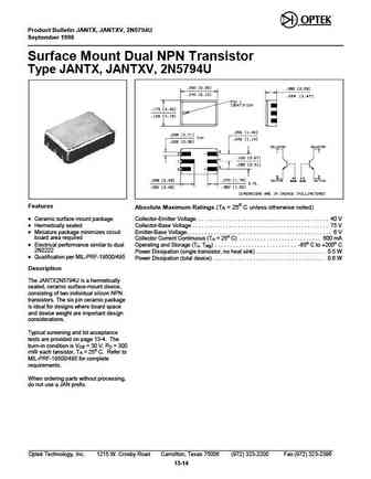
Product Bulletin JANTX, JANTXV, 2N5794U September 1996 Surface Mount Dual NPN Transistor Type JANTX, JANTXV, 2N5794U .058 (1.47) Features Absolute Maximum Ratings (TA = 25o C unless otherwise noted) Ceramic surface mount package Collector-Emitter Voltage. . . . . . . . . . . . . . . . . . . . . . . . . . . . . . . . . . . . . . . . . . . . 40 V Hermetically sealed Collector-Base V
2n5796u.pdf
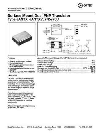
Product Bulletin JANTX, JANTXV, 2N5796U September 1996 Surface Mount Dual PNP Transistor Type JANTX, JANTXV, 2N5796U .058 (1.47) Features Absolute Maximum Ratings (TA = 25o C unless otherwise noted) Collector-Emitter Voltage. . . . . . . . . . . . . . . . . . . . . . . . . . . . . . . . . . . . . . . . . . . . 60 V Ceramic surface mount package Collector-Base Voltage . . . . . . . .
2n5786l.pdf
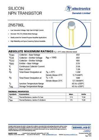
SILICON NPN TRANSISTOR 2N5786L Low Saturation Voltage. High Gain At High Current. Hermetic TO5 (TO-205AA) Metal Package. Ideally suited for General Purpose Amplifier Applications. High Reliability and Space Screening Options Available. ABSOLUTE MAXIMUM RATINGS (TC = 25 C unless otherwise stated) VCBO Collector Base Voltage 45V VCER RBE = 100 Collect
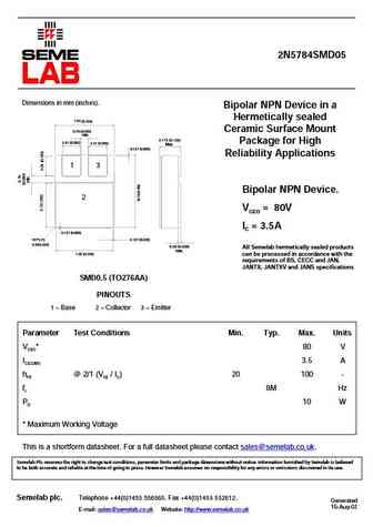
2n5784smd.pdf
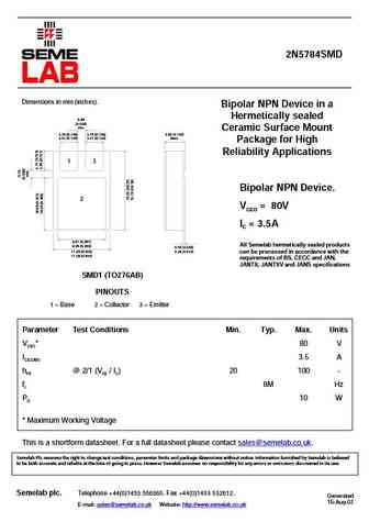
2N5784SMD Dimensions in mm (inches). Bipolar NPN Device in a Hermetically sealed 0.89 (0.035) min. Ceramic Surface Mount 3.70 (0.146) 3.70 (0.146) 3.60 (0.142) 3.41 (0.134) 3.41 (0.134) Max. Package for High Reliability Applications 1 3 Bipolar NPN Device. 2 VCEO = 80V IC = 3.5A 9.67 (0.381) All Semelab hermetically sealed products 9.38 (0.369) 0.50 (0.020) 0.26
2n5785smd.pdf

2N5785SMD Dimensions in mm (inches). Bipolar NPN Device in a Hermetically sealed 0.89 (0.035) min. Ceramic Surface Mount 3.70 (0.146) 3.70 (0.146) 3.60 (0.142) 3.41 (0.134) 3.41 (0.134) Max. Package for High Reliability Applications 1 3 Bipolar NPN Device. 2 VCEO = 65V IC = 3.5A 9.67 (0.381) All Semelab hermetically sealed products 9.38 (0.369) 0.50 (0.020) 0.26
2n5743.pdf
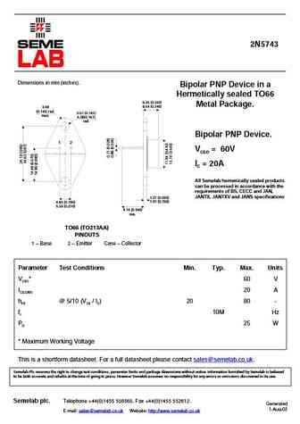
2N5743 Dimensions in mm (inches). Bipolar PNP Device in a Hermetically sealed TO66 6.35 (0.250) Metal Package. 8.64 (0.340) 3.68 (0.145) rad. 3.61 (0.142) max. 4.08(0.161) rad. Bipolar PNP Device. 1 2 VCEO = 60V IC = 20A All Semelab hermetically sealed products can be processed in accordance with the requirements of BS, CECC and JAN, JANTX, JANTXV and JANS speci
2n5759.pdf

2N5759 Dimensions in mm (inches). Bipolar NPN Device in a Hermetically sealed TO3 25.15 (0.99) 6.35 (0.25) 26.67 (1.05) 9.15 (0.36) Metal Package. 10.67 (0.42) 11.18 (0.44) 1.52 (0.06) 3.43 (0.135) 1 2 Bipolar NPN Device. 3 VCEO = 120V (case) 3.84 (0.151) 4.09 (0.161) 7.92 (0.312) IC = 6A 12.70 (0.50) All Semelab hermetically sealed products can be processed in a
2n5781.pdf
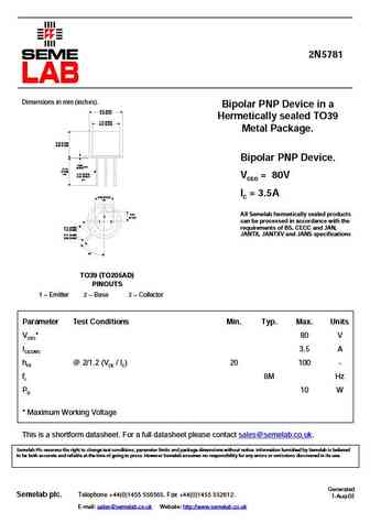
2N5781 Dimensions in mm (inches). Bipolar PNP Device in a 8.51 (0.34) 9.40 (0.37) Hermetically sealed TO39 7.75 (0.305) 8.51 (0.335) Metal Package. 6.10 (0.240) 6.60 (0.260) Bipolar PNP Device. 0.89 max. (0.035) 12.70 (0.500) min. 0.41 (0.016) 0.53 (0.021) VCEO = 80V dia. IC = 3.5A 5.08 (0.200) typ. 2.54 All Semelab hermetically sealed products 2 (0.100) 1
2n5741.pdf
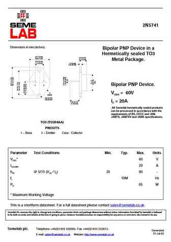
2N5741 Dimensions in mm (inches). Bipolar PNP Device in a Hermetically sealed TO3 25.15 (0.99) 6.35 (0.25) 26.67 (1.05) 9.15 (0.36) Metal Package. 10.67 (0.42) 11.18 (0.44) 1.52 (0.06) 3.43 (0.135) 1 2 Bipolar PNP Device. 3 VCEO = 60V (case) 3.84 (0.151) 4.09 (0.161) 7.92 (0.312) IC = 20A 12.70 (0.50) All Semelab hermetically sealed products can be processed in a
2n5758.pdf
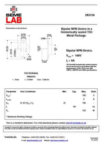
2N5758 Dimensions in mm (inches). Bipolar NPN Device in a Hermetically sealed TO3 25.15 (0.99) 6.35 (0.25) 26.67 (1.05) 9.15 (0.36) Metal Package. 10.67 (0.42) 11.18 (0.44) 1.52 (0.06) 3.43 (0.135) 1 2 Bipolar NPN Device. 3 VCEO = 100V (case) 3.84 (0.151) 4.09 (0.161) 7.92 (0.312) IC = 6A 12.70 (0.50) All Semelab hermetically sealed products can be processed in a
2n5785.pdf

2N5785 Dimensions in mm (inches). Bipolar NPN Device in a 8.51 (0.34) 9.40 (0.37) Hermetically sealed TO39 7.75 (0.305) 8.51 (0.335) Metal Package. 6.10 (0.240) 6.60 (0.260) Bipolar NPN Device. 0.89 max. (0.035) 12.70 (0.500) min. 0.41 (0.016) 0.53 (0.021) VCEO = 65V dia. IC = 3.5A 5.08 (0.200) typ. 2.54 All Semelab hermetically sealed products 2 (0.100) 1
2n5782l.pdf
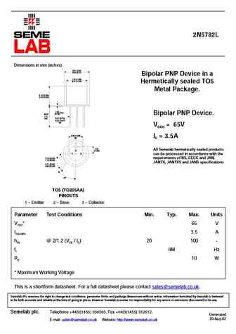
2N5782L Dimensions in mm (inches). 8.51 (0.34) 9.40 (0.37) Bipolar PNP Device in a 7.75 (0.305) 8.51 (0.335) Hermetically sealed TO5 Metal Package. 6.10 (0.240) 6.60 (0.260) 0.89 (0.035)max. 38.00 Bipolar PNP Device. (1.5) 0.41 (0.016) min. 0.53 (0.021) dia. VCEO = 65V 5.08 (0.200) IC = 3.5A typ. 2.54 All Semelab hermetically sealed products 2 (0.100) 1 3 can
2n5781xl.pdf
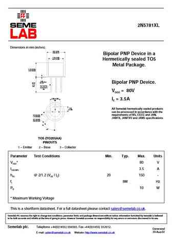
2N5781XL Dimensions in mm (inches). 8.51 (0.34) 9.40 (0.37) Bipolar PNP Device in a 7.75 (0.305) 8.51 (0.335) Hermetically sealed TO5 Metal Package. 6.10 (0.240) 6.60 (0.260) 0.89 (0.035)max. 38.00 Bipolar PNP Device. (1.5) 0.41 (0.016) min. 0.53 (0.021) dia. VCEO = 80V 5.08 (0.200) IC = 3.5A typ. 2.54 All Semelab hermetically sealed products 2 (0.100) 1 3 ca
2n5784.pdf
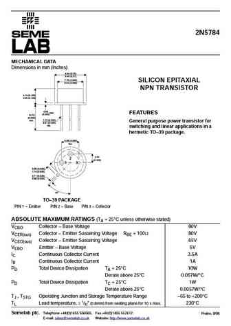
2N5784 MECHANICAL DATA Dimensions in mm (inches) 8.89 (0.35) 9.40 (0.37) 7.75 (0.305) SILICON EPITAXIAL 8.51 (0.335) NPN TRANSISTOR 4.19 (0.165) 4.95 (0.195) 0.89 max. FEATURES (0.035) 12.70 (0.500) 7.75 (0.305) min. General purpose power transistor for 8.51 (0.335) dia. switching and linear applications in a hermetic TO 39 package. 5.08 (0.200) typ. 2.54 2 (0.100)
2n5785smd05.pdf
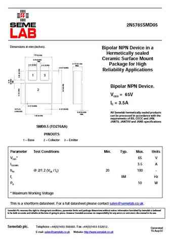
2N5785SMD05 Dimensions in mm (inches). Bipolar NPN Device in a Hermetically sealed 7.54 (0.296) 0.76 (0.030) Ceramic Surface Mount min. 3.175 (0.125) 2.41 (0.095) Package for High 2.41 (0.095) Max. 0.127 (0.005) Reliability Applications 1 3 Bipolar NPN Device. 2 VCEO = 65V IC = 3.5A 0.127 (0.005) 16 PLCS 0.127 (0.005) 0.50(0.020) 0.50 (0.020) All Semelab he
2n5785n1.pdf
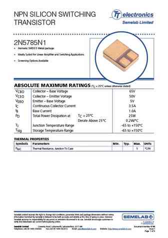
NPN SILICON SWITCHING TRANSISTOR 2N5785N1 Hermetic SMD0.5 Metal package. Ideally Suited for Linear Amplifier and Switching Applications. Screening Options Available ABSOLUTE MAXIMUM RATINGS (TC = 25 C unless otherwise stated) VCBO Collector Base Voltage 65V VCEO Collector Emitter Voltage 50V VEBO Emitter Base Voltage 5V IC Continuous Collecto
2n5784smd05.pdf
2N5784SMD05 Dimensions in mm (inches). Bipolar NPN Device in a Hermetically sealed 7.54 (0.296) 0.76 (0.030) Ceramic Surface Mount min. 3.175 (0.125) 2.41 (0.095) Package for High 2.41 (0.095) Max. 0.127 (0.005) Reliability Applications 1 3 Bipolar NPN Device. 2 VCEO = 80V IC = 3.5A 0.127 (0.005) 16 PLCS 0.127 (0.005) 0.50(0.020) 0.50 (0.020) All Semelab he
2n5770.pdf
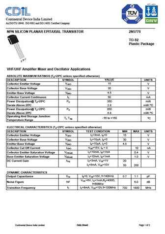
Continental Device India Limited An ISO/TS 16949, ISO 9001 and ISO 14001 Certified Company NPN SILICON PLANAR EPITAXIAL TRANSISTOR 2N5770 TO-92 Plastic Package C B E VHF/UHF Amplifier Mixer and Oscillator Applications ABSOLUTE MAXIMUM RATINGS (Ta=25 C unless specified otherwise) DESCRIPTION SYMBOL VALUE UNITS VCEO Collector Emitter Voltage 15 V Collector Base Voltage VCBO 30 V VE
2n5745.pdf
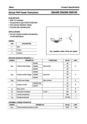
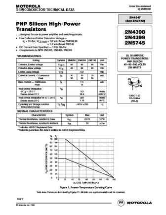
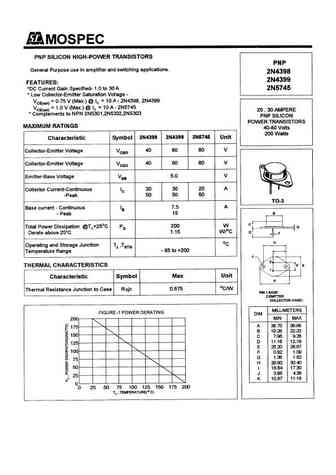
JMnic Product Specification Silicon PNP Power Transistors 2N4398 2N4399 2N5745 DESCRIPTION With TO-3 package Complement to type 2N5301/5302/5303 Low collector saturation voltage Excellent safe operating area APPLICATIONS For use in power amplifier and switching circuits applications. PINNING PIN DESCRIPTION 1 Base 2 Emitter Fig.1 simplified outline (TO-3) and
2n5741 2n5742.pdf
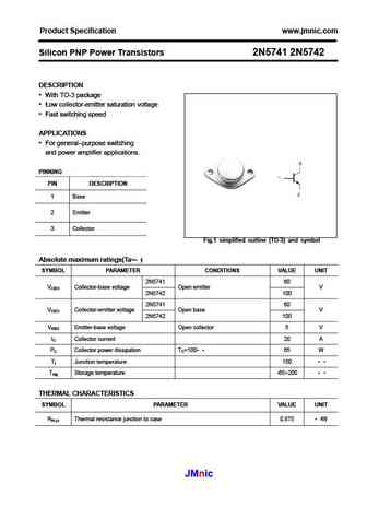
Product Specification www.jmnic.com Silicon PNP Power Transistors 2N5741 2N5742 DESCRIPTION With TO-3 package Low collector-emitter saturation voltage Fast switching speed APPLICATIONS For general purpose switching and power amplifier applications. PINNING PIN DESCRIPTION 1 Base 2 Emitter 3 Collector Fig.1 simplified outline (TO-3) and symbol Absolute maximu
2n5758 2n5759 2n5760.pdf
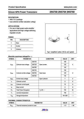
Product Specification www.jmnic.com Silicon NPN Power Transistors 2N5758 2N5759 2N5760 DESCRIPTION With TO-3 package Low collector-emitter saturation voltage APPLICATIONS For use in high power audio amplifier applications and high voltage switching regulator circuits PINNING PIN DESCRIPTION 1 Base 2 Emitter 3 Collector Fig.1 simplified outline (TO-3) and symbol
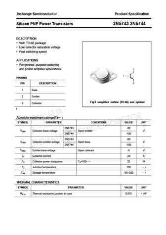
2n5743 2n5744.pdf
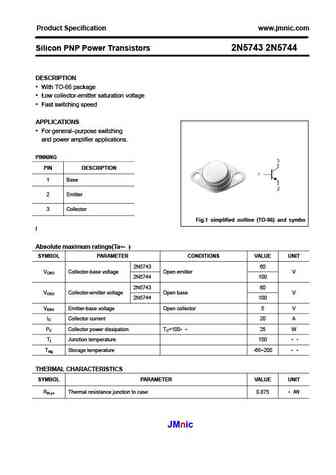
Product Specification www.jmnic.com Silicon PNP Power Transistors 2N5743 2N5744 DESCRIPTION With TO-66 package Low collector-emitter saturation voltage Fast switching speed APPLICATIONS For general purpose switching and power amplifier applications. PINNING PIN DESCRIPTION 1 Base 2 Emitter 3 Collector Fig.1 simplified outline (TO-66) and symbo l Absolute ma
2n5794u.pdf
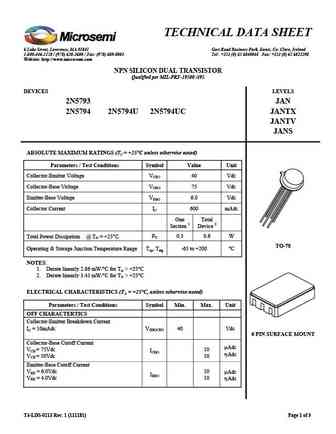
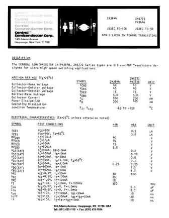
TECHNICAL DATA SHEET 6 Lake Street, Lawrence, MA 01841 6 Lake Street, Lawrence, MA 01841 Gort Road Business Park, Ennis, Co. Clare, Ireland 1-800-446-1158 / (978) 620-2600 / Fax (978) 689-0803 Tel +353 (0) 65 6840044 Fax +353 (0) 65 6822298 Website http //www.microsemi.com NPN SILICON DUAL TRANSISTOR Qualified per MIL-PRF-19500 /495 DEVICES LEVELS 2N5793 JAN 2N5794 2N5794U
2n5795-96.pdf

TECHNICAL DATA PNP DUAL SILICON TRANSISTOR Qualified per MIL-PRF-19500/496 Devices Qualified Level JAN 2N5796 2N5795 JANTX 2N5796U JANTXV MAXIMUM RATINGS Ratings Symbol Value Units Collector-Emitter Voltage 60 Vdc VCEO Collector-Base Voltage 60 Vdc VCBO Emitter-Base Voltage 5.0 Vdc VEBO TO-78* Collector Current 600 mAdc IC Both(2) One(1) Section Sections
2n5794uc 2n5794uc 2n5794u.pdf

TECHNICAL DATA SHEET 6 Lake Street, Lawrence, MA 01841 6 Lake Street, Lawrence, MA 01841 Gort Road Business Park, Ennis, Co. Clare, Ireland 1-800-446-1158 / (978) 620-2600 / Fax (978) 689-0803 Tel +353 (0) 65 6840044 Fax +353 (0) 65 6822298 Website http //www.microsemi.com NPN SILICON DUAL TRANSISTOR Qualified per MIL-PRF-19500 /495 DEVICES LEVELS 2N5793 JAN 2N5794 2N5794U
2n5796u.pdf
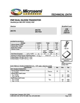
TECHNICAL DATA PNP DUAL SILICON TRANSISTOR Qualified per MIL-PRF-19500/496 Devices Qualified Level JAN 2N5796 2N5795 JANTX 2N5796U JANTXV MAXIMUM RATINGS Ratings Symbol Value Units Collector-Emitter Voltage 60 Vdc VCEO Collector-Base Voltage 60 Vdc VCBO Emitter-Base Voltage 5.0 Vdc VEBO TO-78* Collector Current 600 mAdc IC Both(2) One(1) Section Sections
2n5744.pdf
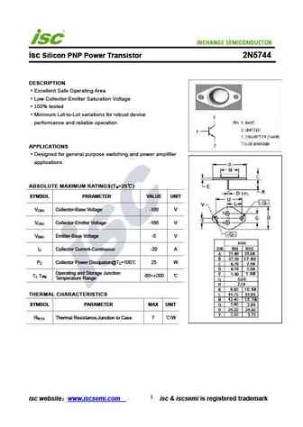
INCHANGE Semiconductor isc Silicon PNP Power Transistor 2N5744 DESCRIPTION Excellent Safe Operating Area Low Collector-Emitter Saturation Voltage 100% tested Minimum Lot-to-Lot variations for robust device performance and reliable operation APPLICATIONS Designed for general purpose switching and power amplifier applications ABSOLUTE MAXIMUM RATINGS(T =25 ) a SYMBOL PARA
2n5741 2n5742.pdf

Inchange Semiconductor Product Specification Silicon PNP Power Transistors 2N5741 2N5742 DESCRIPTION With TO-3 package Low collector saturation voltage Fast switching speed APPLICATIONS For general purpose switching and power amplifier applications. PINNING PIN DESCRIPTION 1 Base 2 Emitter Fig.1 simplified outline (TO-3) and symbol 3 Collector Absolute maximu
2n5739.pdf

INCHANGE Semiconductor isc Product Specification isc Silicon PNP Power Transistors 2N5739 DESCRIPTION Collector-Emitter Sustaining Voltage- VCEO(SUS)= -60V(Min.) Low Collector Saturation Voltage- VCE(sat)= -0.5V(Max.)@ IC= -5A Wide Area of Safe Operation APPLICATIONS Designed for general-purpose power amplifier and switching applications. ABSOLUTE MAXIMUM RAT
2n5732.pdf
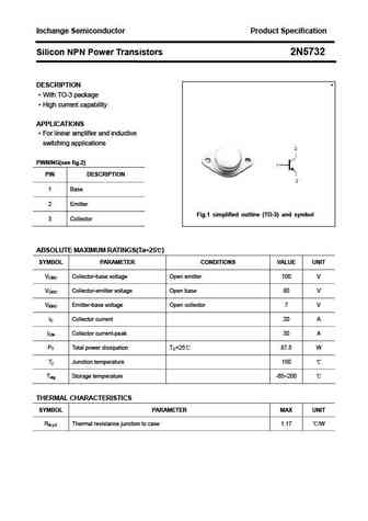
Inchange Semiconductor Product Specification Silicon NPN Power Transistors 2N5732 DESCRIPTION With TO-3 package High current capability APPLICATIONS For linear amplifier and inductive switching applications PINNING(see fig.2) PIN DESCRIPTION 1 Base 2 Emitter Fig.1 simplified outline (TO-3) and symbol 3 Collector ABSOLUTE MAXIMUM RATINGS(Ta=25 ) SYMBOL PARAME
2n5743.pdf
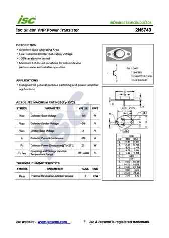
isc Silicon PNP Power Transistor 2N5743 DESCRIPTION Excellent Safe Operating Area Low Collector-Emitter Saturation Voltage 100% avalanche tested Minimum Lot-to-Lot variations for robust device performance and reliable operation APPLICATIONS Designed for general purpose switching and power amplifier applications ABSOLUTE MAXIMUM RATINGS(T =25 ) a SYMBOL PARAMETER VALUE UN
2n5738.pdf

INCHANGE Semiconductor isc Product Specification isc Silicon PNP Power Transistors 2N5738 DESCRIPTION Collector-Emitter Sustaining Voltage- VCEO(SUS)= -100V(Min.) Low Collector Saturation Voltage- VCE(sat)= -0.5V(Max.)@ IC= -5A Wide Area of Safe Operation APPLICATIONS Designed for general-purpose power amplifier and switching applications. ABSOLUTE MAXIMUM RA
2n5758 2n5759 2n5760.pdf
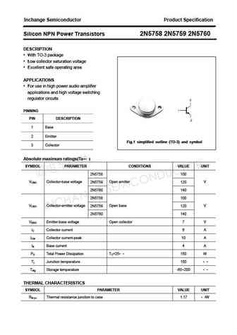
Inchange Semiconductor Product Specification Silicon NPN Power Transistors 2N5758 2N5759 2N5760 DESCRIPTION With TO-3 package Low collector saturation voltage Excellent safe operating area APPLICATIONS For use in high power audio amplifier applications and high voltage switching regulator circuits PINNING PIN DESCRIPTION 1 Base 2 Emitter Fig.1 simplified outlin
2n5737.pdf
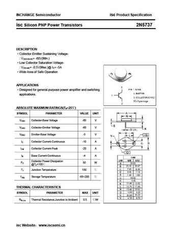
INCHANGE Semiconductor isc Product Specification isc Silicon PNP Power Transistors 2N5737 DESCRIPTION Collector-Emitter Sustaining Voltage- VCEO(SUS)= -60V(Min.) Low Collector Saturation Voltage- VCE(sat)= -0.5V(Max.)@ IC= -5A Wide Area of Safe Operation APPLICATIONS Designed for general-purpose power amplifier and switching applications. ABSOLUTE MAXIMUM RAT
2n4398 2n4399 2n5745.pdf
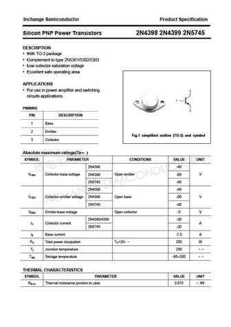
Inchange Semiconductor Product Specification Silicon PNP Power Transistors 2N4398 2N4399 2N5745 DESCRIPTION With TO-3 package Complement to type 2N5301/5302/5303 Low collector saturation voltage Excellent safe operating area APPLICATIONS For use in power amplifier and switching circuits applications. PINNING PIN DESCRIPTION 1 Base 2 Emitter Fig.1 simplified o
2n5743 2n5744.pdf
Inchange Semiconductor Product Specification Silicon PNP Power Transistors 2N5743 2N5744 DESCRIPTION With TO-66 package Low collector saturation voltage Fast switching speed APPLICATIONS For general purpose switching and power amplifier applications. PINNING PIN DESCRIPTION 1 Base 2 Emitter Fig.1 simplified outline (TO-66) and symbol 3 Collector l Absolute
2n5734.pdf
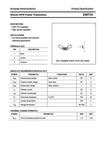
Inchange Semiconductor Product Specification Silicon NPN Power Transistors 2N5734 DESCRIPTION With TO-3 package High current capability APPLICATIONS For linear amplifier and inductive switching applications PINNING(see fig.2) PIN DESCRIPTION 1 Base 2 Emitter Fig.1 simplified outline (TO-3) and symbol 3 Collector ABSOLUTE MAXIMUM RATINGS(Ta=25 ) SYMBOL PARAME
2n5740.pdf

INCHANGE Semiconductor isc Product Specification isc Silicon PNP Power Transistors 2N5740 DESCRIPTION Collector-Emitter Sustaining Voltage- VCEO(SUS)= -100V(Min.) Low Collector Saturation Voltage- VCE(sat)= -0.5V(Max.)@ IC= -5A Wide Area of Safe Operation APPLICATIONS Designed for general-purpose power amplifier and switching applications. ABSOLUTE MAXIMUM RA
Другие транзисторы: 2N5692, 2N5693, 2N5694, 2N5695, 2N5696, 2N5697, 2N5698, 2N5699, 2N3904, 2N570, 2N5700, 2N5701, 2N5702, 2N5703, 2N5704, 2N5705, 2N5706
History: 2N1624 | LMBT3904DW1T1G | BSR60 | BF262 | EFT332 | 2N1657 | 2N162A
🌐 : EN ES РУ

Список транзисторов
Обновления
BJT: GA1A4M | SBT42 | 2SA200-Y | 2SA200-O | 2SD882-Q | 2SD882-P | 2SD882-E | 2SC945-L | 2SC945-H | 2SC4226-R23 | 2SC3357-F | 2SC3357-E | 2SC3356-R26 | 2SC3356-R24 | 2SC3356-R23 | 2SB772-Q | 2SB772-P | 2SB772-E | 2SA1015-L | 2SA1015-H | HSS8550
Popular searches
2sc1079 | 2sc1815 equivalent | 2sa1220 | 2sa940 | 2sc627 | 2sc680 | 2sd234 | 2sc9014