CN1 datasheet, аналоги, основные параметры
Наименование производителя: CN1 📄📄
Тип материала: Si
Полярность: NPN
Предельные значения
Максимальная рассеиваемая мощность (Pc): 0.4 W
Макcимально допустимое напряжение коллектор-база (Ucb): 12 V
Макcимально допустимое напряжение коллектор-эмиттер (Uce): 12 V
Макcимально допустимое напряжение эмиттер-база (Ueb): 4.5 V
Макcимальный постоянный ток коллектора (Ic): 0.15 A
Предельная температура PN-перехода (Tj): 125 °C
Электрические характеристики
Статический коэффициент передачи тока (hFE): 50
Корпус транзистора: TO-92
📄📄 Копировать
Аналоги (замена) для CN1
- подборⓘ биполярного транзистора по параметрам
CN1 даташит
cn1 cp4.pdf
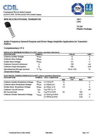
Q Continental Device India Limited An ISO/TS 16949, ISO 9001 and ISO 14001 Certified Company NPN SILICON EPITAXIAL TRANSISTOR CN 1 CP4 TO-92 Plastic Package Audio Frequency General Purpose and Driver Stage Amplofier Application for Transistor Radios. Complementary CP 4 ABSOLUTE MAXIMUM RATINGS (Ta=25 C unless specified otherwise) DESCRIPTION SYMBOL VALUE UNIT BVCEO Collector Emit
ipd64cn10ng ipu64cn10ng.pdf
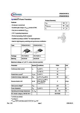
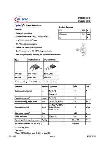
$ " " $( " " $;B1= '=- >5>?;= $=;0@/? &@99-=D Features 100 V DS S ( 5 3@@7> @AD?3> >7H7> 64 m DS(on) max S J57>>7@F 93F7 5 3D97 J BDA6G5F !) ' DS(on) 17 A D S 07DK >AI A@ D7E;EF3@57 DS(on) S V AB7D3F;@9 F7?B7D3FGD7 S *4 8D77 >736 B>3F;@9 , A#- 5A?B>;3@F 1) S + G3>;8;76 355AD6;@9 FA % 8AD F3D97F 3BB>;53F;A@ S $673> 8AD ;9 8D7CG7@5K EI;F5 ;@9 3@6 EK@5 DA@AGE D
ipb08cn10ng ipi08cn10ng ipp08cn10ng.pdf
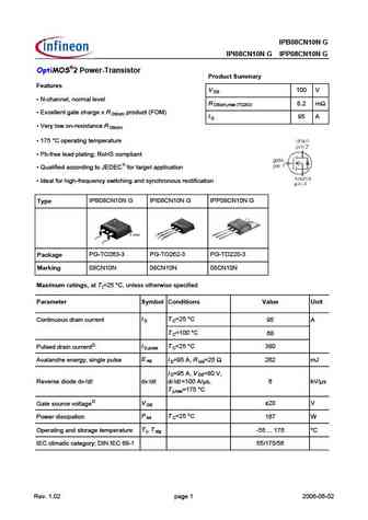
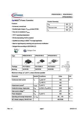
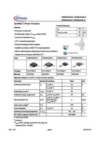
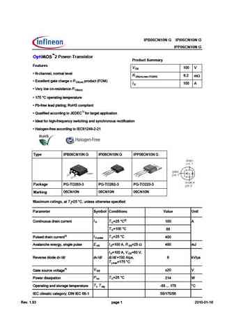
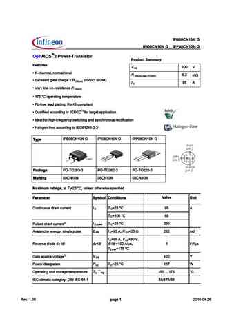
IPB08CN10N G IPI08CN10N G IPP08CN10N G OptiMOS 2 Power-Transistor Product Summary Features V 100 V DS N-channel, normal level R 8.2 m DS(on),max (TO263) Excellent gate charge x R product (FOM) DS(on) I 95 A D Very low on-resistance R DS(on) 175 C operating temperature Pb-free lead plating; RoHS compliant Qualified according to JEDEC1) for target
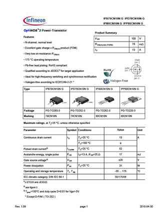
ipb80cn10n ipd78cn10n ipi80cn10n ipp80cn10n ipu78cn10n.pdf
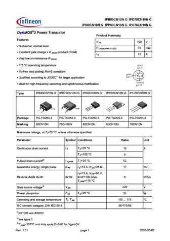
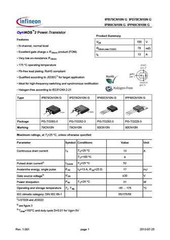
IPB80CN10N G IPD78CN10N G IPI80CN10N G IPP80CN10N G IPU78CN10N G OptiMOS 2 Power-Transistor Product Summary Features V 100 V DS N-channel, normal level R 78 m DS(on),max (TO252) Excellent gate charge x R product (FOM) DS(on) I 13 A D Very low on-resistance R DS(on) 175 C operating temperature Pb-free lead plating; RoHS compliant Qualified accordi
ipb12cn10ng ipd12cn10ng ipi12cn10ng ipp12cn10ng ipb12cn10ng ipi12cn10ng.pdf
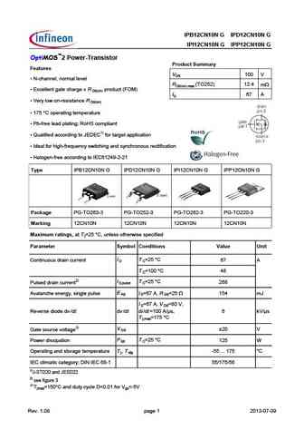
IPB12CN10N G IPD12CN10N G IPI12CN10N G IPP12CN10N G OptiMOS 2 Power-Transistor Product Summary Features VDS 100 V N-channel, normal level RDS(on),max (TO252) 12.4 mW Excellent gate charge x R product (FOM) DS(on) ID 67 A Very low on-resistance R DS(on) 175 C operating temperature Pb-free lead plating; RoHS compliant Qualified according to JEDEC1)
ipb12cn10n-g ipd12cn10n-g ipi12cn10n-g ipp12cn10n-g.pdf
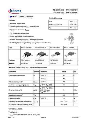
IPB12CN10N G IPD12CN10N G IPI12CN10N G IPP12CN10N G OptiMOS 2 Power-Transistor Product Summary Features V 100 V DS N-channel, normal level R (TO252) 12.4 m DS(on),max Excellent gate charge x R product (FOM) DS(on) I 67 A D Very low on-resistance R DS(on) 175 C operating temperature Pb-free lead plating; RoHS compliant Qualified according to JEDEC
ipb04cn10ng ipi04cn10n ipp04cn10n.pdf
IPB04CN10N G IPI04CN10N G IPP04CN10N G 2 Power-Transistor Product Summary Features V 1 D R ( 492??6= ?@C>2= =6G6= R m - @? >2I .) R I46==6?E 82E6 492C86 I R AC@5F4E !) ' D n) I 1 D R /6CJ =@H @? C6D DE2?46 R D n) R U @A6C2E ?8 E6>A6C2EFC6 R *3 7C66 =625 A=2E ?8 , @#- 4@>A= 2?E 1) R + F2= 7 65 244@C5 ?8 E@ % 7@C E2C86E 2AA= 42E @? R $562= 7@C 9 89 7C6BF6?4J DH E4
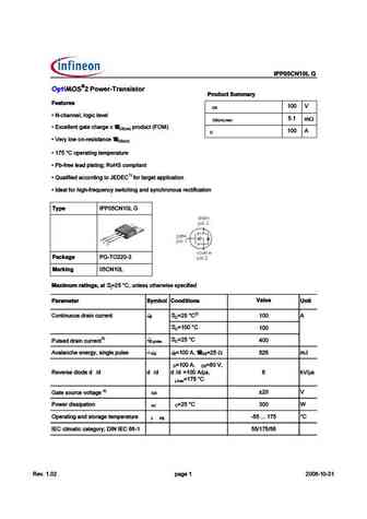
ipp05cn10n ipp05cn10n ipb05cn10n-g ipi05cn10n-g.pdf
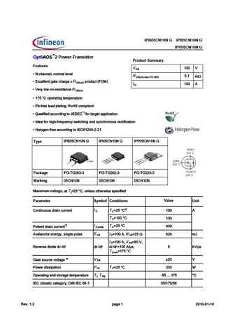
IPB05CN10N G IPI05CN10N G IPP05CN10N G 2 Power-Transistor Product Summary Features V 100 V DS R ( 492??6= ?@C>2= =6G6= R 5.1 m - @? >2I .) R I46==6?E 82E6 492C86 I R AC@5F4E !) ' DS(on) I 100 A D R /6CJ =@H @? C6D DE2?46 R DS(on) R U @A6C2E ?8 E6>A6C2EFC6 R *3 7C66 =625 A=2E ?8 , @#- 4@>A= 2?E 1) R + F2= 7 65 244@C5 ?8 E@ % 7@C E2C86E 2AA= 42E @? R $562= 7@C 9 89 7
ipb50cn10ng ipd49cn10ng ipi50cn10ng ipp50cn10ng.pdf
$ " " $ " " $ " " $$ " " $;B1= '=- >5>?;= $=;0@/? &@99-=D Features 1 D S ) 5 3@@7> @AD?3> >7H7> 4 m . A@ ?3J /* S !J57>>7@F 93F7 5 3D97 J BDA6G5F "* ( D n) D S 07DK >AI A@ D7E;EF3@57 D n) S V AB7D3F;@9 F7?B7D3FGD7 S +4 8D77 >736 B>3F;@9 - A$. 5A?B>;3@F 1) S , G3>;8;76 355AD6;@9 FA &! ! 8AD F3D97F 3BB>;53F;A@ S %673> 8AD ;9 8D7CG7@5K EI;F5 ;@9 3@6 EK@5 DA@AGE
ipb06cn10n-g ipi06cn10n-g ipp06cn10n-g.pdf
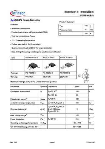
IPB06CN10N G IPI06CN10N G IPP06CN10N G OptiMOS 2 Power-Transistor Product Summary Features V 100 V DS N-channel, normal level R 6.2 m DS(on),max (TO263) Excellent gate charge x R product (FOM) DS(on) I 100 A D Very low on-resistance R DS(on) 175 C operating temperature Pb-free lead plating; RoHS compliant Qualified according to JEDEC1) for target
ipp08cn10l1.pdf
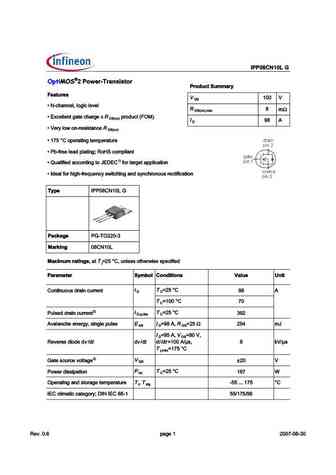
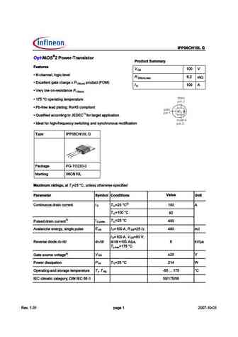
IPP08CN10L G 2 Power-Transistor Product Summary Features V 100 V DS N-channel, logic level R 8 m DS(on),max Excellent gate charge x R product (FOM) DS(on) I 98 A D Very low on-resistance R DS(on) 175 C operating temperature Pb-free lead plating; RoHS compliant Qualified according to JEDEC1) for target application Ideal for high-frequency
ipb26cn10ng ipd25cn10ng ipi26cn10ng ipp26cn10ng.pdf
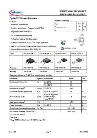
IPB26CN10N G IPD25CN10N G IPI26CN10N G IPP26CN10N G OptiMOS 2 Power-Transistor Product Summary Features VDS 100 V N-channel, normal level RDS(on),max (TO252) 25 mW Excellent gate charge x R product (FOM) DS(on) ID 35 A Very low on-resistance R DS(on) 175 C operating temperature Pb-free lead plating; RoHS compliant Qualified according to JEDEC1)
ipb79cn10n-g ipd78cn10n-g ipi80cn10n-g ipp80cn10n-g.pdf
IPB79CN10N G IPD78CN10N G IPI80CN10N G IPP80CN10N G OptiMOS 2 Power-Transistor Product Summary Features V 100 V DS N-channel, normal level R 78 m DS(on),max (TO252) Excellent gate charge x R product (FOM) DS(on) I 13 A D Very low on-resistance R DS(on) 175 C operating temperature Pb-free lead plating; RoHS compliant Qualified according to JEDEC
ipp16cn10l1.pdf
%% # ! % (>.;?6?@ %>E Features 1 D S ) 5 3@@7> >A9;5 >7H7> 1 7 m . A@ ?3J S J57>>7@F 93F7 5 3D97 J BDA6G5F !* ( D n) 4 D S 07DK >AI A@ D7E;EF3@57 D n) S V AB7D3F;@9 F7?B7D3FGD7 S +4 8D77 >736 B>3F;@9 - A#. 5A?B>;3@F 1) S , G3>;8;76 355AD6;@9 FA % 8AD F3D97F 3BB>;53F;A@ S $673> 8AD ;9 8D7CG7@5K EI;F5 ;@9 3@6 EK@5 DA@AGE D75F;8;53F;A@ Type
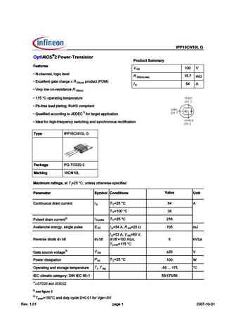
ipb16cn10n ipd16cn10n ipi16cn10n ipp16cn10n.pdf
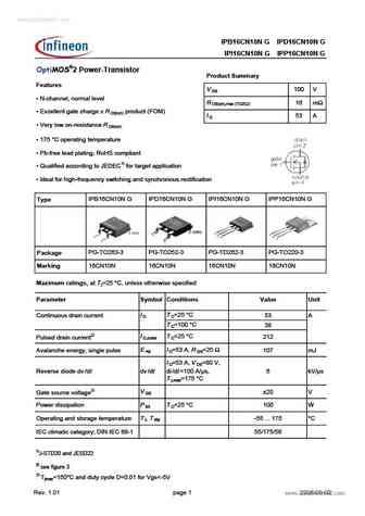
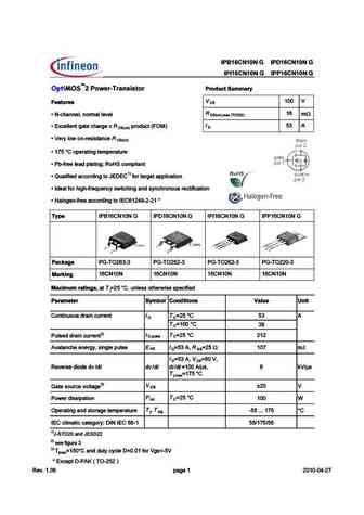
www.DataSheet4U.com IPB16CN10N G IPD16CN10N G IPI16CN10N G IPP16CN10N G OptiMOS 2 Power-Transistor Product Summary Features V 100 V DS N-channel, normal level R 16 m DS(on),max (TO252) Excellent gate charge x R product (FOM) DS(on) I 53 A D Very low on-resistance R DS(on) 175 C operating temperature Pb-free lead plating; RoHS compliant Qualified
ipp06cn10n.pdf
IPB06CN10N G IPI06CN10N G IPP06CN10N G 2 Power-Transistor Product Summary Features V 100 V DS R ( 492??6= ?@C>2= =6G6= R 6.2 m - @? >2I .) R I46==6?E 82E6 492C86 I R AC@5F4E !) ' DS(on) I 100 A D R /6CJ =@H @? C6D DE2?46 R DS(on) R U @A6C2E ?8 E6>A6C2EFC6 R *3 7C66 =625 A=2E ?8 , @#- 4@>A= 2?E 1) R + F2= 7 65 244@C5 ?8 E@ % 7@C E2C86E 2AA= 42E @? R $562= 7@C 9 89 7
ipb16cn10ng ipd16cn10ng ipi16cn10ng ipp16cn10ng.pdf
$ " " $ " " $ " " $$ " " $;B1= '=- >5>?;= $=;0@/? &@99-=D 1 Features D 1 m S ) 5 3@@7> @AD?3> >7H7> . A@ ?3J /* S !J57>>7@F 93F7 5 3D97 J BDA6G5F "* ( D D n) S 07DK >AI A@ D7E;EF3@57 D n) S V AB7D3F;@9 F7?B7D3FGD7 S +4 8D77 >736 B>3F;@9 - A$. 5A?B>;3@F 1) S , G3>;8;76 355AD6;@9 FA &! ! 8AD F3D97F 3BB>;53F;A@ S %673> 8AD ;9 8D7CG7@5K EI;F5 ;@9 3@6 EK@5 DA@AGE D7
ipb34cn10ng ipd33cn10ng ipi35cn10ng ipp35cn10ng ipb34cn10n ipd33cn10n ipi35cn10n ipp35cn10n.pdf
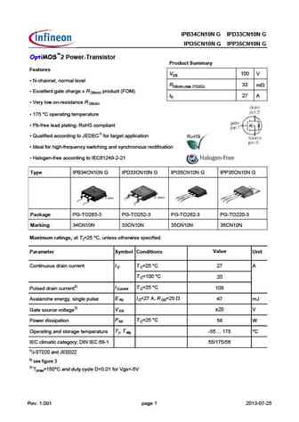
IPB34CN10N G IPD33CN10N G IPI35CN10N G IPP35CN10N G OptiMOS 2 Power-Transistor Product Summary Features VDS 100 V N-channel, normal level RDS(on),max (TO252) 33 mW Excellent gate charge x R product (FOM) DS(on) ID 27 A Very low on-resistance R DS(on) 175 C operating temperature Pb-free lead plating; RoHS compliant Qualified according to JEDEC1) f
ipb04cn10ng ipi04cn10ng ipp04cn10ng ipp04cn10n .pdf

IPB04CN10N G IPI04CN10N G IPP04CN10N G 2 Power-Transistor Product Summary Features V 1 D R ( 492??6= ?@C>2= =6G6= R m - @? >2I .) R I46==6?E 82E6 492C86 I R AC@5F4E !) ' D n) I 1 D R /6CJ =@H @? C6D DE2?46 R D n) R U @A6C2E ?8 E6>A6C2EFC6 R *3 7C66 =625 A=2E ?8 , @#- 4@>A= 2?E 1) R + F2= 7 65 244@C5 ?8 E@ % 7@C E2C86E 2AA= 42E @? R $562= 7@C 9 89 7C6BF6?4J DH E4
ipb26cn10n-g ipd25cn10n-g ipi26cn10n-g ipp26cn10n-g ipu25cn10n-g.pdf

IPB26CN10N G IPD25CN10N G IPI26CN10N G IPP26CN10N G IPU25CN10N G OptiMOS 2 Power-Transistor Product Summary Features V 100 V DS N-channel, normal level R 25 m DS(on),max (TO252) Excellent gate charge x R product (FOM) DS(on) I 35 A D Very low on-resistance R DS(on) 175 C operating temperature Pb-free lead plating; RoHS compliant Qualified accordi
ipp12cn10l-g ips12cn10l-g.pdf
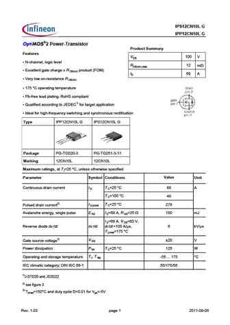
IPS12CN10L G IPP12CN10L G OptiMOS 2 Power-Transistor Product Summary Features VDS 100 V N-channel, logic level RDS(on),max 12 mW Excellent gate charge x R product (FOM) DS(on) ID 69 A Very low on-resistance R DS(on) 175 C operating temperature Pb-free lead plating; RoHS compliant Qualified according to JEDEC1) for target application Ideal for high
ipp64cn10n2.pdf
$ " " $( " " $;B1= '=- >5>?;= $=;0@/? &@99-=D Features 100 V DS S ( 5 3@@7> @AD?3> >7H7> 64 m DS(on) max S J57>>7@F 93F7 5 3D97 J BDA6G5F !) ' DS(on) 17 A D S 07DK >AI A@ D7E;EF3@57 DS(on) S V AB7D3F;@9 F7?B7D3FGD7 S *4 8D77 >736 B>3F;@9 , A#- 5A?B>;3@F 1) S + G3>;8;76 355AD6;@9 FA % 8AD F3D97F 3BB>;53F;A@ S $673> 8AD ;9 8D7CG7@5K EI;F5 ;@9 3@6 EK@5 DA@AGE D
ipp08cn10n8.pdf
$ " " $ " " $$ " " $;B1= '=- >5>?;= $=;0@/? &@99-=D Features 100 V DS R ( 492??6= ?@C>2= =6G6= 8.2 m - @? >2I .) R I46==6?E 82E6 492C86 I AC@5F4E !) ' DS(on) 95 A D R /6CJ =@H @? C6D DE2?46 DS(on) R U @A6C2E ?8 E6>A6C2EFC6 R *3 7C66 =625 A=2E ?8 , @#- 4@>A= 2?E 1) R + F2= 7 65 244@C5 ?8 E@ % 7@C E2C86E 2AA= 42E @? R $562= 7@C 9 89 7C6BF6?4J DH E49 ?8 2?5 DJ?49C@
ipb35cn10n-g ipd33cn10n-g ipi35cn10n-g ipp35cn10n-g ipu33cn10n-g.pdf

IPB35CN10N G IPD33CN10N G IPI35CN10N G IPP35CN10N G IPU33CN10N G OptiMOS 2 Power-Transistor Product Summary Features V 100 V DS N-channel, normal level R 34 m DS(on),max (TO252) Excellent gate charge x R product (FOM) DS(on) I 27 A D Very low on-resistance R DS(on) 175 C operating temperature Pb-free lead plating; RoHS compliant Qualified accordi
ipb79cn10ng ipd78cn10ng ipi80cn10ng ipp80cn10ng.pdf
IPB79CN10N G IPD78CN10N G IPI80CN10N G IPP80CN10N G OptiMOS 2 Power-Transistor Product Summary Features VDS 100 V N-channel, normal level RDS(on),max (TO252) 78 mW Excellent gate charge x R product (FOM) DS(on) ID 13 A Very low on-resistance R DS(on) 175 C operating temperature Pb-free lead plating; RoHS compliant Qualified according to JEDEC1)
ipp06cn10l1.pdf
%% # ! % (>.;?6?@ %>E Features 1 D S ) 5 3@@7> >A9;5 >7H7> m . A@ ?3J S J57>>7@F 93F7 5 3D97 J BDA6G5F !* ( D n) 1 D S 07DK >AI A@ D7E;EF3@57 D n) S V AB7D3F;@9 F7?B7D3FGD7 S +4 8D77 >736 B>3F;@9 - A#. 5A?B>;3@F 1) S , G3>;8;76 355AD6;@9 FA % 8AD F3D97F 3BB>;53F;A@ S $673> 8AD ;9 8D7CG7@5K EI;F5 ;@9 3@6 EK@5 DA@AGE D75F;8;53F;A@ pe $++
cn1933.pdf
Continental Device India Limited An ISO/TS 16949, ISO 9001 and ISO 14001 Certified Company NPN SILICON PLASTIC POWER DARLINGTON TRANSISTOR CN1933 (9AW) TO-220 MARKING CN 1933 Low Freq. Power Amp. Built in Damper Diode Complementry CP1342 ABSOLUTE MAXIMUM RATINGS(Ta=25deg C) DESCRIPTION SYMBOL VALUE UNIT Collector -Base Voltage VCBO 80 V Collector -Emitter Voltage VCEO 80 V Emitte
cn1016.pdf
Continental Device India Limited An ISO/TS 16949, ISO 9001 and ISO 14001 Certified Company NPN SILICON PLASTIC POWER DARLINGTON TRANSISTOR CN1016 (9AW) TO-3P MARKING - CN 1016 ABSOLUTE MAXIMUM RATINGS(Ta=25deg C) DESCRIPTION SYMBOL VALUE UNIT Collector -Base Voltage VCBO 160 V Collector -Emitter Voltage VCEO 150 V Emitter Base Voltage VEBO 5.0 V Collector Current IC 10 A Peak t=30m
cn107.pdf
Continental Device India Limited An ISO/TS 16949, ISO 9001 and ISO 14001 Certified Company NPN EPITAXIAL PLANAR SILICON TRANSISTOR CN 107 TO-92 CBE ABSOLUTE MAXIMUM RATINGS DESCRIPTION SYMBOL VALUE UNIT Collector -Base Voltage VCBO 60 V Collector -Emitter Voltage VCEO 50 V Emitter Base Voltage VEBO 6.0 V Collector Current Continuous IC 100 mA Peak ICM 200 mA Total Power Dissipation
ipd78cn10n.pdf
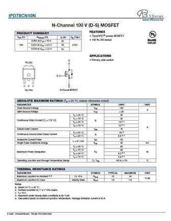
IPD78CN10N www.VBsemi.tw N-Channel 100 V (D-S) MOSFET FEATURES PRODUCT SUMMARY TrenchFET power MOSFET VDS (V) RDS(on) ( )ID (A) Qg (Typ.) 100 % UIS tested 0.055 at VGS = 10 V 25 0.057 at VGS = 4.5 V 100 25 21nC 0.070 at VGS = 2.5 V 18 APPLICATIONS Primary side switch D TO-252 G G D S S N-Channel MOSFET Top View ABSOLUTE MAXIMUM RATINGS (TA = 25 C, unl
ipb26cn10n.pdf

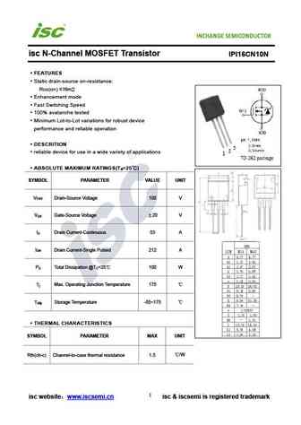
Isc N-Channel MOSFET Transistor IPB26CN10N FEATURES With To-263(D2PAK) package Low input capacitance and gate charge Low gate input resistance 100% avalanche tested Minimum Lot-to-Lot variations for robust device performance and reliable operation APPLICATIONS Switching applications ABSOLUTE MAXIMUM RATINGS(T =25 ) a SYMBOL PARAMETER VALUE UNIT V Drain-Source Vo
ipp12cn10n.pdf
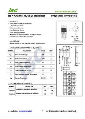
INCHANGE Semiconductor isc N-Channel MOSFET Transistor IPP12CN10N IIPP12CN10N FEATURES Static drain-source on-resistance RDS(on) 12.9m Enhancement mode Fast Switching Speed 100% avalanche tested Minimum Lot-to-Lot variations for robust device performance and reliable operation DESCRITION reliable device for use in a wide variety of applications ABSOLUTE MA
ipb16cn10ng.pdf
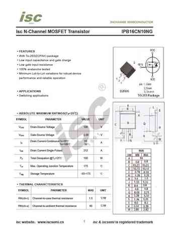
Isc N-Channel MOSFET Transistor IPB16CN10NG FEATURES With To-263(D2PAK) package Low input capacitance and gate charge Low gate input resistance 100% avalanche tested Minimum Lot-to-Lot variations for robust device performance and reliable operation APPLICATIONS Switching applications ABSOLUTE MAXIMUM RATINGS(T =25 ) a SYMBOL PARAMETER VALUE UNIT V Drain-Source V
ipd33cn10n.pdf

isc N-Channel MOSFET Transistor IPD33CN10N,IIPD33CN10N FEATURES Static drain-source on-resistance RDS(on) 34m Enhancement mode 100% avalanche tested Minimum Lot-to-Lot variations for robust device performance and reliable operation DESCRITION Ideal for high-frequency switching and synchronous rectification ABSOLUTE MAXIMUM RATINGS(T =25 ) a SYMBOL PARAMETER
ipi35cn10n.pdf
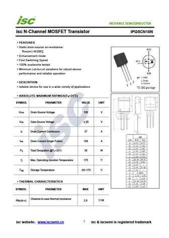
INCHANGE Semiconductor isc N-Channel MOSFET Transistor IPI35CN10N FEATURES Static drain-source on-resistance RDS(on) 0.035 Enhancement mode Fast Switching Speed 100% avalanche tested Minimum Lot-to-Lot variations for robust device performance and reliable operation DESCRITION reliable device for use in a wide variety of applications ABSOLUTE MAXIMUM RATINGS(
ipd78cn10n.pdf
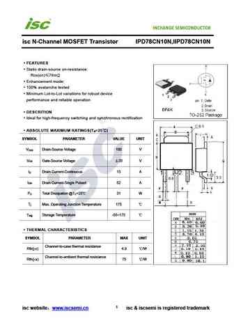
isc N-Channel MOSFET Transistor IPD78CN10N,IIPD78CN10N FEATURES Static drain-source on-resistance RDS(on) 78m Enhancement mode 100% avalanche tested Minimum Lot-to-Lot variations for robust device performance and reliable operation DESCRITION Ideal for high-frequency switching and synchronous rectification ABSOLUTE MAXIMUM RATINGS(T =25 ) a SYMBOL PARAMETER
ipi80cn10n.pdf
INCHANGE Semiconductor isc N-Channel MOSFET Transistor IPI80CN10N FEATURES Static drain-source on-resistance RDS(on) 0.08 Enhancement mode Fast Switching Speed 100% avalanche tested Minimum Lot-to-Lot variations for robust device performance and reliable operation DESCRITION reliable device for use in a wide variety of applications ABSOLUTE MAXIMUM RATINGS(T
ipb79cn10ng.pdf

Isc N-Channel MOSFET Transistor IPB79CN10NG FEATURES With To-263(D2PAK) package Low input capacitance and gate charge Low gate input resistance 100% avalanche tested Minimum Lot-to-Lot variations for robust device performance and reliable operation APPLICATIONS Switching applications ABSOLUTE MAXIMUM RATINGS(T =25 ) a SYMBOL PARAMETER VALUE UNIT V Drain-Source V
ipp16cn10n.pdf
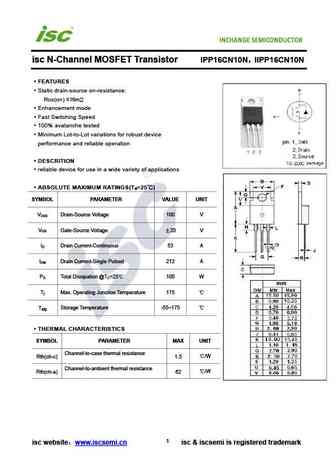
isc N-Channel MOSFET Transistor IPP16CN10N IIPP16CN10N FEATURES Static drain-source on-resistance RDS(on) 16m Enhancement mode Fast Switching Speed 100% avalanche tested Minimum Lot-to-Lot variations for robust device performance and reliable operation DESCRITION reliable device for use in a wide variety of applications ABSOLUTE MAXIMUM RATINGS(T =25 ) a
ipp26cn10n.pdf

INCHANGE Semiconductor isc N-Channel MOSFET Transistor IPP26CN10N IIPP26CN10N FEATURES Static drain-source on-resistance RDS(on) 26m Enhancement mode Fast Switching Speed 100% avalanche tested Minimum Lot-to-Lot variations for robust device performance and reliable operation DESCRITION reliable device for use in a wide variety of applications ABSOLUTE MAXI
ipd25cn10n.pdf

isc N-Channel MOSFET Transistor IPD25CN10N,IIPD25CN10N FEATURES Static drain-source on-resistance RDS(on) 25m Enhancement mode 100% avalanche tested Minimum Lot-to-Lot variations for robust device performance and reliable operation DESCRITION Ideal for high-frequency switching and synchronous rectification ABSOLUTE MAXIMUM RATINGS(T =25 ) a SYMBOL PARAMETER
ipp35cn10n.pdf
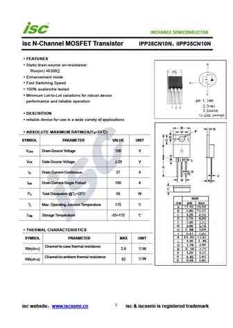
INCHANGE Semiconductor isc N-Channel MOSFET Transistor IPP35CN10N IIPP35CN10N FEATURES Static drain-source on-resistance RDS(on) 0.035 Enhancement mode Fast Switching Speed 100% avalanche tested Minimum Lot-to-Lot variations for robust device performance and reliable operation DESCRITION reliable device for use in a wide variety of applications ABSOLUTE MA
ipi26cn10n.pdf
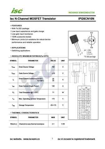
Isc N-Channel MOSFET Transistor IPI26CN10N FEATURES With To-262 package Low input capacitance and gate charge Low gate input resistance 100% avalanche tested Minimum Lot-to-Lot variations for robust device performance and reliable operation APPLICATIONS Switching applications ABSOLUTE MAXIMUM RATINGS(T =25 ) a SYMBOL PARAMETER VALUE UNIT V Drain-Source Voltage 1
ipb12cn10ng.pdf

Isc N-Channel MOSFET Transistor IPB12CN10NG FEATURES With To-263(D2PAK) package Low input capacitance and gate charge Low gate input resistance 100% avalanche tested Minimum Lot-to-Lot variations for robust device performance and reliable operation APPLICATIONS Switching applications ABSOLUTE MAXIMUM RATINGS(T =25 ) a SYMBOL PARAMETER VALUE UNIT V Drain-Source V
ipi05cn10n.pdf
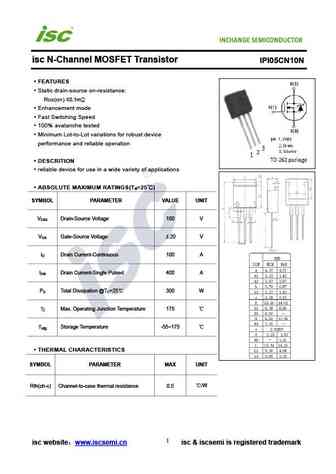
isc N-Channel MOSFET Transistor IPI05CN10N FEATURES Static drain-source on-resistance RDS(on) 5.1m Enhancement mode Fast Switching Speed 100% avalanche tested Minimum Lot-to-Lot variations for robust device performance and reliable operation DESCRITION reliable device for use in a wide variety of applications ABSOLUTE MAXIMUM RATINGS(T =25 ) a SYMBOL PARA
ipd16cn10n.pdf

isc N-Channel MOSFET Transistor IPD16CN10N,IIPD16CN10N FEATURES Static drain-source on-resistance RDS(on) 16m Enhancement mode 100% avalanche tested Minimum Lot-to-Lot variations for robust device performance and reliable operation DESCRITION Ideal for high-frequency switching and synchronous rectification ABSOLUTE MAXIMUM RATINGS(T =25 ) a SYMBOL PARAMETER
ipp04cn10n.pdf
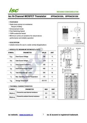
NCHANGE Semicon Iductor isc N-Channel MOSFET Transistor IPP04CN10N IIPP04CN10N FEATURES Static drain-source on-resistance RDS(on) 3.9m Enhancement mode Fast Switching Speed 100% avalanche tested Minimum Lot-to-Lot variations for robust device performance and reliable operation DESCRITION reliable device for use in a wide variety of applications ABSOLUTE MA
ipi04cn10n.pdf

NCHANGE Semicon Iductor isc N-Channel MOSFET Transistor IPI04CN10N FEATURES Static drain-source on-resistance RDS(on) 3.9m Enhancement mode Fast Switching Speed 100% avalanche tested Minimum Lot-to-Lot variations for robust device performance and reliable operation DESCRITION reliable device for use in a wide variety of applications ABSOLUTE MAXIMUM RATINGS(
ipi12cn10ng.pdf
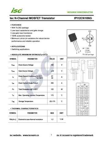
Isc N-Channel MOSFET Transistor IPI12CN10NG FEATURES With To-262 package Low input capacitance and gate charge Low gate input resistance 100% avalanche tested Minimum Lot-to-Lot variations for robust device performance and reliable operation APPLICATIONS Switching applications ABSOLUTE MAXIMUM RATINGS(T =25 ) a SYMBOL PARAMETER VALUE UNIT V Drain-Source Voltage
ipp80cn10n.pdf

INCHANGE Semiconductor isc N-Channel MOSFET Transistor IPP80CN10N IIPP80CN10N FEATURES Static drain-source on-resistance RDS(on) 0.08 Enhancement mode Fast Switching Speed 100% avalanche tested Minimum Lot-to-Lot variations for robust device performance and reliable operation DESCRITION reliable device for use in a wide variety of applications ABSOLUTE MAX
ipi16cn10n.pdf
isc N-Channel MOSFET Transistor IPI16CN10N FEATURES Static drain-source on-resistance RDS(on) 16m Enhancement mode Fast Switching Speed 100% avalanche tested Minimum Lot-to-Lot variations for robust device performance and reliable operation DESCRITION reliable device for use in a wide variety of applications ABSOLUTE MAXIMUM RATINGS(T =25 ) a SYMBOL PARAM
ipb04cn10ng.pdf

Isc N-Channel MOSFET Transistor IPB04CN10NG FEATURES With To-263(D2PAK) package Low input capacitance and gate charge Low gate input resistance 100% avalanche tested Minimum Lot-to-Lot variations for robust device performance and reliable operation APPLICATIONS Switching applications ABSOLUTE MAXIMUM RATINGS(T =25 ) a SYMBOL PARAMETER VALUE UNIT V Drain-Source V
ipp05cn10n.pdf

isc N-Channel MOSFET Transistor IPP05CN10N IIPP05CN10N FEATURES Static drain-source on-resistance RDS(on) 5.1m Enhancement mode Fast Switching Speed 100% avalanche tested Minimum Lot-to-Lot variations for robust device performance and reliable operation DESCRITION reliable device for use in a wide variety of applications ABSOLUTE MAXIMUM RATINGS(T =25 )
ipb05cn10n.pdf

Isc N-Channel MOSFET Transistor IPB05CN10N FEATURES With To-263(D2PAK) package Low input capacitance and gate charge Low gate input resistance 100% avalanche tested Minimum Lot-to-Lot variations for robust device performance and reliable operation APPLICATIONS Switching applications ABSOLUTE MAXIMUM RATINGS(T =25 ) a SYMBOL PARAMETER VALUE UNIT V Drain-Source Vo
ips12cn10l.pdf
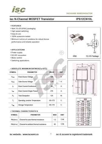
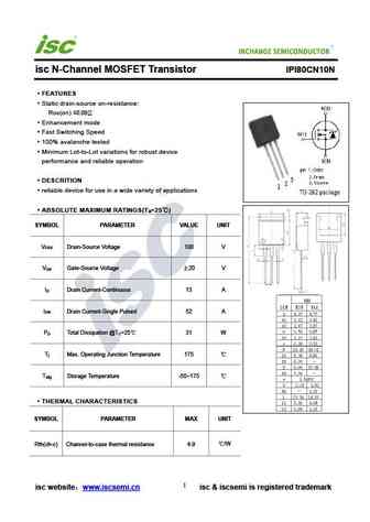
isc N-Channel MOSFET Transistor IPS12CN10L FEATURES With TO-251(IPAK) packaging High speed switching Easy to use 100% avalanche tested Minimum Lot-to-Lot variations for robust device performance and reliable operation APPLICATIONS Power supply DC-DC converters Motor control Switching applications ABSOLUTE MAXIMUM RATINGS(T =25 ) a SYMBOL PARAMETER VALUE
ipb34cn10n.pdf

Isc N-Channel MOSFET Transistor IPB34CN10N FEATURES With To-263(D2PAK) package Low input capacitance and gate charge Low gate input resistance 100% avalanche tested Minimum Lot-to-Lot variations for robust device performance and reliable operation APPLICATIONS Switching applications ABSOLUTE MAXIMUM RATINGS(T =25 ) a SYMBOL PARAMETER VALUE UNIT V Drain-Source Vo
ipp12cn10l.pdf

isc N-Channel MOSFET Transistor IPP12CN10L IIPP12CN10L FEATURES Static drain-source on-resistance RDS(on) 12m Enhancement mode Fast Switching Speed 100% avalanche tested Minimum Lot-to-Lot variations for robust device performance and reliable operation DESCRITION reliable device for use in a wide variety of applications ABSOLUTE MAXIMUM RATINGS(T =25 ) a
Другие транзисторы: CML1207, CMMT451, CMMT491, CMMT493, CMMT495, CMMT551, CMMT591, CMMT591A, BD679, CN102, CN107, CN1933, CN300, CN301, CN302, CN303, CN304
Параметры биполярного транзистора и их взаимосвязь

Список транзисторов
Обновления
BJT: ZDT6705 | GA1L4Z | GA1A4M | SBT42 | 2SA200-Y | 2SA200-O | 2SD882-Q | 2SD882-P | 2SD882-E | 2SC945-L | 2SC945-H | 2SC4226-R23 | 2SC3357-F | 2SC3357-E | 2SC3356-R26 | 2SC3356-R24 | 2SC3356-R23 | 2SB772-Q | 2SB772-P | 2SB772-E | 2SA1015-L
Popular searches
irfb7437 | tip32a | p75nf75 mosfet equivalent | irfpe50 | tip50 | transistor bc547 datasheet | bc109c | d331 transistor