D667 datasheet, аналоги, основные параметры
Наименование производителя: D667 📄📄
Тип материала: Si
Полярность: NPN
Предельные значения
Максимальная рассеиваемая мощность (Pc): 0.8 W
Макcимально допустимое напряжение коллектор-база (Ucb): 60 V
Макcимально допустимое напряжение коллектор-эмиттер (Uce): 40 V
Макcимально допустимое напряжение эмиттер-база (Ueb): 5 V
Макcимальный постоянный ток коллектора (Ic): 2 A
Предельная температура PN-перехода (Tj): 150 °C
Электрические характеристики
Граничная частота коэффициента передачи тока (ft): 50 MHz
Статический коэффициент передачи тока (hFE): 100
Корпус транзистора: TO92
📄📄 Копировать
Аналоги (замена) для D667
- подборⓘ биполярного транзистора по параметрам
D667 даташит
..1. Size:113K jdsemi
d667.pdf 
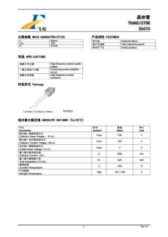
R D667 www.jdsemi.cn Bipolar Junction Transistor ShenZhen Jingdao Electronic Co.,Ltd. Si NPN RoHS COMPLIANT 1 1 1 APPLICATION 1 Charger Emergency lamp and Electric toy control circuit 2 2 2 FEATURES 2
0.1. Size:117K fairchild semi
fdd6676s.pdf 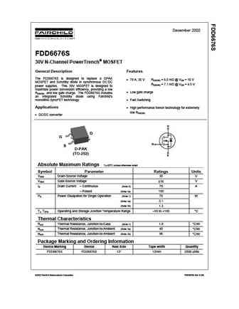
December 2002 FDD6676S 30V N-Channel PowerTrench MOSFET General Description Features The FDS6676S is designed to replace a DPAK 78 A, 30 V RDS(ON) = 6.0 m @ VGS = 10 V MOSFET and Schottky diode in synchronous DC DC RDS(ON) = 7.1 m @ VGS = 4.5 V power supplies. This 30V MOSFET is designed to maximize power conversion efficiency, providing a low Low gate charge
0.2. Size:91K fairchild semi
fdd6670s.pdf 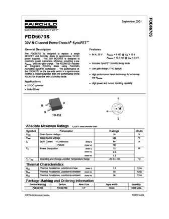
September 2001 FDD6670S 30V N-Channel PowerTrench SyncFET General Description Features The FDD6670S is designed to replace a single 64 A, 30 V RDS(ON) = 9 m @ VGS = 10 V MOSFET and Schottky diode in synchronous DC DC RDS(ON) = 12.5 m @ VGS = 4.5 V power supplies. This 30V MOSFET is designed to maximize power conversion efficiency, providing a low Includes S
0.3. Size:147K fairchild semi
fdd6670al.pdf 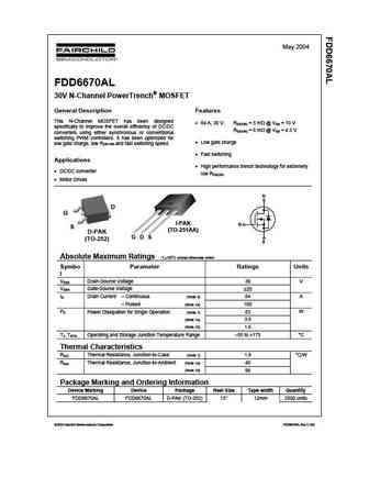
May 2004 FDD6670AL 30V N-Channel PowerTrench MOSFET General Description Features This N-Channel MOSFET has been designed 84 A, 30 V. RDS(ON) = 5 m @ VGS = 10 V specifically to improve the overall efficiency of DC/DC RDS(ON) = 6 m @ VGS = 4.5 V converters using either synchronous or conventional switching PWM controllers. It has been optimized for Low gate c
0.4. Size:80K fairchild semi
fdd6676.pdf 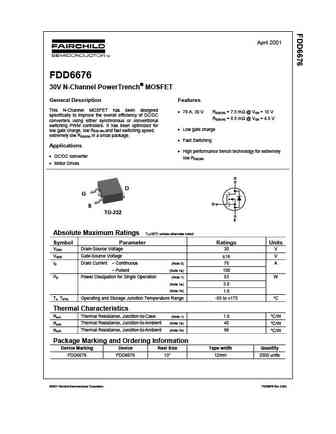
April 2001 FDD6676 30V N-Channel PowerTrench MOSFET General Description Features This N-Channel MOSFET has been designed 78 A, 30 V RDS(ON) = 7.5 m @ VGS = 10 V specifically to improve the overall efficiency of DC/DC RDS(ON) = 8.5 m @ VGS = 4.5 V converters using either synchronous or conventional switching PWM controllers. It has been optimized for
0.5. Size:105K fairchild semi
fdd6670as.pdf 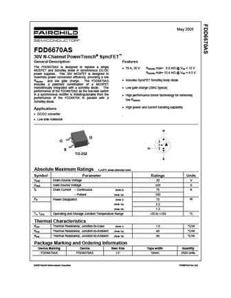
May 2005 FDD6670AS 30V N-Channel PowerTrench SyncFET General Description Features The FDD6670AS is designed to replace a single 76 A, 30 V RDS(ON) max= 8.0 m @ VGS = 10 V MOSFET and Schottky diode in synchronous DC DC RDS(ON) max= 10.4 m @ VGS = 4.5 V power supplies. This 30V MOSFET is designed to maximize power conversion efficiency, providing a low Inclu
0.6. Size:76K fairchild semi
fdd6672a.pdf 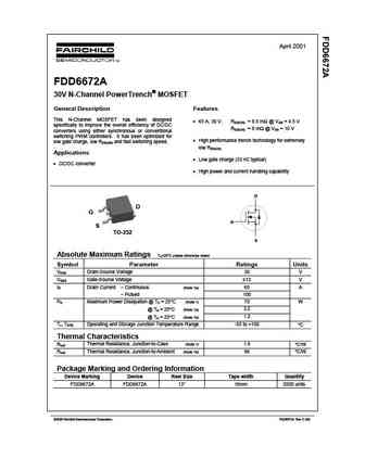
April 2001 FDD6672A 30V N-Channel PowerTrench MOSFET General Description Features This N-Channel MOSFET has been designed 65 A, 30 V. RDS(ON) = 9.5 m @ VGS = 4.5 V specifically to improve the overall efficiency of DC/DC RDS(ON) = 8 m @ VGS = 10 V converters using either synchronous or conventional switching PWM controllers. It has been optimized for
0.7. Size:109K fairchild semi
fdd6670a.pdf 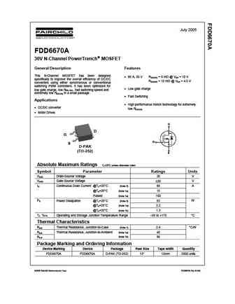
July 2005 FDD6670A 30V N-Channel PowerTrench MOSFET General Description Features This N-Channel MOSFET has been designed 66 A, 30 V RDS(ON) = 8 m @ VGS = 10 V specifically to improve the overall efficiency of DC/DC RDS(ON) = 10 m @ VGS = 4.5 V converters using either synchronous or conventional switching PWM controllers. It has been optimized for Low gate charge low ga
0.8. Size:411K fairchild semi
fdd6676as.pdf 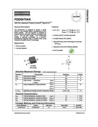
April 2008 FDD6676AS tm 30V N-Channel PowerTrench SyncFET General Description Features The FDD6676AS is designed to replace a single 90 A, 30 V RDS(ON) = 5.7 m @ VGS = 10 V MOSFET and Schottky diode in synchronous DC DC RDS(ON) = 7.1 m @ VGS = 4.5 V power supplies. This 30V MOSFET is designed to maximize power conversion efficiency, providing a low Includ
0.9. Size:284K mcc
2sd667l.pdf 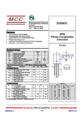
MCC TM Micro Commercial Components 20736 Marilla Street Chatsworth 2SD667L Micro Commercial Components CA 91311 Phone (818) 701-4933 Fax (818) 701-4939 Features Low Frequency Power Amplifier NPN Complementary Pair with 2SB647/A Plastic-Encapsulate Epoxy meets UL 94 V-0 flammability rating Moisture Sensitivity Level 1 Transistor Lead Free Finish/Rohs Compl
0.10. Size:557K mcc
2sd667a-b-c-d 2sd667-b-c-d.pdf 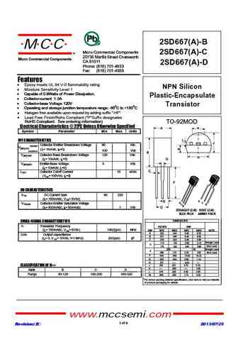
2SD667(A)-B MCC Micro Commercial Components TM 2SD667(A)-C 20736 Marilla Street Chatsworth Micro Commercial Components CA 91311 2SD667(A)-D Phone (818) 701-4933 Fax (818) 701-4939 Features Epoxy meets UL 94 V-0 flammability rating NPN Silicon Moisture Sensitivity Level 1 Capable of 0.9Watts of Power Dissipation. Capable of 0.9Watts of Power Dissipation. Pla
0.11. Size:331K utc
2sd667.pdf 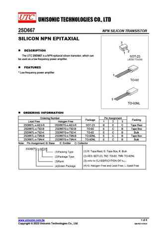
UNISONIC TECHNOLOGIES CO., LTD 2SD667 NPN SILICON TRANSISTOR SILICON NPN EPITAXIAL DESCRIPTION The UTC 2SD667 is a NPN epitaxial silicon transistor, which can be used as a low frequency power amplifier. FEATURES * Low frequency power amplifier ORDERING INFORMATION Ordering Number Pin Assignment Package Packing Lead Free Halogen Free 1 2 3 2SD667L-x-AE3-R 2SD6
0.12. Size:32K hitachi
2sd667.pdf 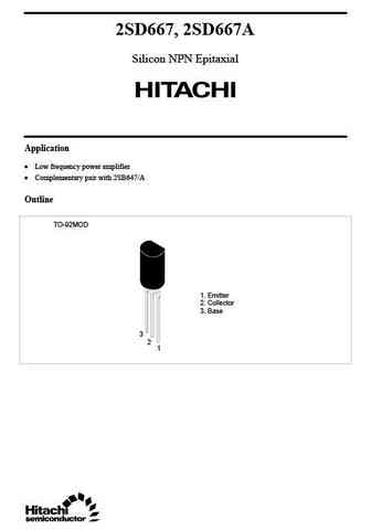
2SD667, 2SD667A Silicon NPN Epitaxial Application Low frequency power amplifier Complementary pair with 2SB647/A Outline TO-92MOD 1. Emitter 2. Collector 3. Base 3 2 1 2SD667, 2SD667A Absolute Maximum Ratings (Ta = 25 C) Item Symbol 2SD667 2SD667A Unit Collector to base voltage VCBO 120 120 V Collector to emitter voltage VCEO 80 100 V Emitter to base voltage VEBO 55V
0.13. Size:64K secos
2sd667a.pdf 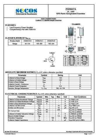
2SD667A 1A , 120V NPN Plastic Encapsulated Transistor Elektronische Bauelemente RoHS Compliant Product A suffix of -C specifies halogen & lead-free TO-92MOD FEATURES A D Low Frequency Power Amplifier Complementary Pair with 2SB647A B K E F CLASSIFICATION OF hFE (1) C Product-Rank 2SD667A-B 2SD667A-C 2SD667A-D Range 60 120 100 200 160 320 N G H 1 Emitte
0.14. Size:118K cdil
cld667 a.pdf 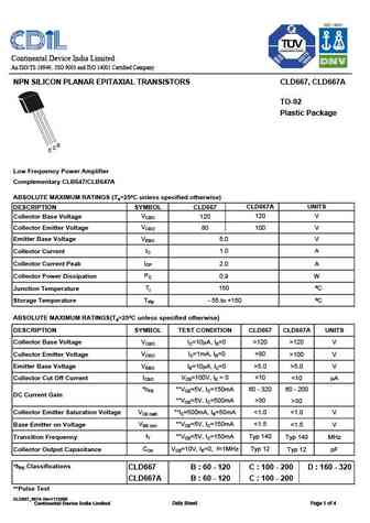
Continental Device India Limited An ISO/TS 16949, ISO 9001 and ISO 14001 Certified Company NPN SILICON PLANAR EPITAXIAL TRANSISTORS CLD667, CLD667A TO-92 Plastic Package B C E Low Frequency Power Amplifier Complementary CLB647/CLB647A ABSOLUTE MAXIMUM RATINGS (Ta=25 C unless specified otherwise) DESCRIPTION SYMBOL CLD667 CLD667A UNITS VCBO Collector Base Voltage 120 120 V VCEO C
0.15. Size:547K jiangsu
2sd667 2sd667a.pdf 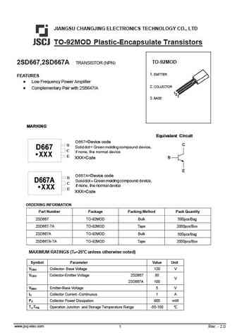
JIANGSU CHANGJING ELECTRONICS TECHNOLOGY CO., LTD TO-92MOD Plastic-Encapsulate Transistors TO-92MOD 2SD667,2SD667A TRANSISTOR (NPN) 1. EMITTER FEATURES Low Frequency Power Amplifier 2. COLLECTOR Complementary Pair with 2SB647/A 3. BASE Equivalent Circuit D667=Device code Solid dot = Green molding compound device, D667 if none, the normal device XXX=Code
0.16. Size:257K lge
2sd667-2sd667a to-92mod.pdf 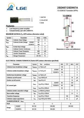
2SD667/2SD667A TO-92MOD Transistor (NPN) TO-92MOD 1. EMITTER 1 2 2. COLLECTOR 3 3. BASE Features Low frequency power amplifier 5.800 6.200 Complementary pair with 2SB647/A 8.400 MAXIMUM RATINGS (TA=25 unless otherwise noted) 8.800 0.900 1.100 Symbol Parameter Value Units 0.400 VCBO Collector- Base Voltage 120 V 0.600 VCEO Collector-Emitter Voltage 2SD667 8
0.17. Size:215K lge
2sd667-2sd667a to-92l.pdf 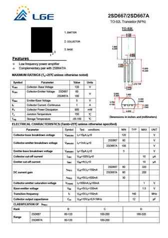
2SD667/2SD667A TO-92L Transistor (NPN) TO-92L 1. EMITTER 2. COLLECTOR 3. BASE 4.700 5.100 2 3 1 Features 7.800 Low frequency power amplifier 8.200 Complementary pair with 2SB647/A 0.600 0.800 MAXIMUM RATINGS (TA=25 unless otherwise noted) 0.350 Symbol Parameter Value Units 0.550 13.800 14.200 VCBO Collector- Base Voltage 120 V VCEO Collector-Emitter Vol
0.18. Size:49K hsmc
hsd667a.pdf 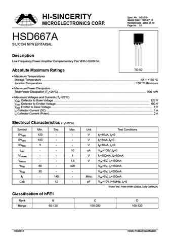
Spec. No. HE6510 HI-SINCERITY Issued Date 1996.07.15 Revised Date 2004.08.16 MICROELECTRONICS CORP. Page No. 1/5 HSD667A SILICON NPN EPITAXIAL Description Low Frequency Power Amplifier Complementary Pair With HSB647A. TO-92 Absolute Maximum Ratings Maximum Temperatures Storage Temperature ..................................................................................
0.19. Size:897K blue-rocket-elect
2sd667 2sd667a.pdf 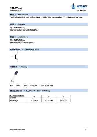
2SD667(A) Rev.F Mar.-2016 DATA SHEET / Descriptions TO-92LM NPN Silicon NPN transistor in a TO-92LM Plastic Package. / Features 2SB647(A) Complementary pair with 2SB647(A). / Applications Low frequency power amplifier. / Equivalent Circuit / P
0.20. Size:557K blue-rocket-elect
2sd667a.pdf 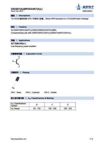
2SD667(A)(BR3DG667(A)L) Rev.C Feb.-2015 DATA SHEET / Descriptions TO-92LM NPN Silicon NPN transistor in a TO-92LM Plastic Package. / Features 2SB647(BR3CG647L)/2SB647A(BR3CG647AL) Complementary pair with 2SB647(BR3CG647L)/2SB647A(BR3CG647AL). / Applications Low frequency power ampli
0.22. Size:287K inchange semiconductor
fdd6676s.pdf 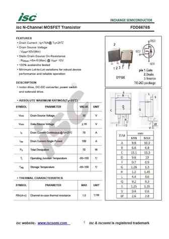
isc N-Channel MOSFET Transistor FDD6676S FEATURES Drain Current I =78A@ T =25 D C Drain Source Voltage V =30V(Min) DSS Static Drain-Source On-Resistance R =6m (Max) @ V = 10V DS(on) GS 100% avalanche tested Minimum Lot-to-Lot variations for robust device performance and reliable operation DESCRIPTION motor drive, DC-DC converter, power switch and solenoid dr
0.23. Size:308K inchange semiconductor
fdd6670s.pdf 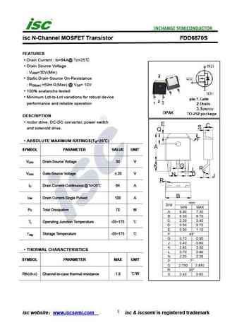
isc N-Channel MOSFET Transistor FDD6670S FEATURES Drain Current I =64A@ T =25 D C Drain Source Voltage V =30V(Min) DSS Static Drain-Source On-Resistance R =59m (Max) @ V = 10V DS(on) GS 100% avalanche tested Minimum Lot-to-Lot variations for robust device performance and reliable operation DESCRIPTION motor drive, DC-DC converter, power switch and solenoid d
0.24. Size:308K inchange semiconductor
fdd6670al.pdf 
isc N-Channel MOSFET Transistor FDD6670AL FEATURES Drain Current I =84A@ T =25 D C Drain Source Voltage V =30V(Min) DSS Static Drain-Source On-Resistance R =5m (Max) @ V = 10V DS(on) GS 100% avalanche tested Minimum Lot-to-Lot variations for robust device performance and reliable operation DESCRIPTION motor drive, DC-DC converter, power switch and solenoid d
0.25. Size:287K inchange semiconductor
fdd6676.pdf 
isc N-Channel MOSFET Transistor FDD6676 FEATURES Drain Current I =78A@ T =25 D C Drain Source Voltage V =30V(Min) DSS Static Drain-Source On-Resistance R =7.5m (Max) @ V = 10V DS(on) GS 100% avalanche tested Minimum Lot-to-Lot variations for robust device performance and reliable operation DESCRIPTION motor drive, DC-DC converter, power switch and solenoid d
0.26. Size:287K inchange semiconductor
fdd6672a.pdf 
isc N-Channel MOSFET Transistor FDD6672A FEATURES Drain Current I =65A@ T =25 D C Drain Source Voltage V =30V(Min) DSS Static Drain-Source On-Resistance R =8m (Max) @ V = 10V DS(on) GS 100% avalanche tested Minimum Lot-to-Lot variations for robust device performance and reliable operation DESCRIPTION motor drive, DC-DC converter, power switch and solenoid dr
0.27. Size:308K inchange semiconductor
fdd6670a.pdf 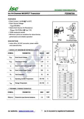
isc N-Channel MOSFET Transistor FDD6670A FEATURES Drain Current I =66A@ T =25 D C Drain Source Voltage V =30V(Min) DSS Static Drain-Source On-Resistance R =8m (Max) @ V = 10V DS(on) GS 100% avalanche tested Minimum Lot-to-Lot variations for robust device performance and reliable operation DESCRIPTION motor drive, DC-DC converter, power switch and solenoid dr
Другие транзисторы: BU3150F-A, BU3150T, BU5027A, BU5027AF, BU5027S, BU6084B, BU6084BF, BU8403, BD139, D880, D882P, D882PC, DBU103T, DK52, DK52A, DK52D, DK53AD