2N66 datasheet, аналоги, основные параметры
Наименование производителя: 2N66 📄📄
Тип материала: Ge
Полярность: PNP
Предельные значения
Максимальная рассеиваемая мощность (Pc): 1 W
Макcимально допустимое напряжение коллектор-база (Ucb): 40 V
Макcимально допустимое напряжение коллектор-эмиттер (Uce): 40 V
Макcимальный постоянный ток коллектора (Ic): 0.8 A
Предельная температура PN-перехода (Tj): 80 °C
Электрические характеристики
Граничная частота коэффициента передачи тока (ft): 0.1 MHz
Корпус транзистора: MM1
📄📄 Копировать
Аналоги (замена) для 2N66
- подборⓘ биполярного транзистора по параметрам
2N66 даташит
2n6667 2n6668.pdf
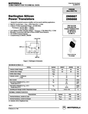
Order this document MOTOROLA by 2N6667/D SEMICONDUCTOR TECHNICAL DATA 2N6609 (See 2N3773) Darlington Silicon 2N6667 Power Transistors 2N6668 . . . designed for general purpose amplifier and low speed switching applications. High DC Current Gain hFE = 3500 (Typ) @ IC = 4 Adc PNP SILICON Collector Emitter Sustaining Voltage @ 200 mAdc DARLINGTON VCEO(sus) = 60 V
2n3773 2n6609.pdf
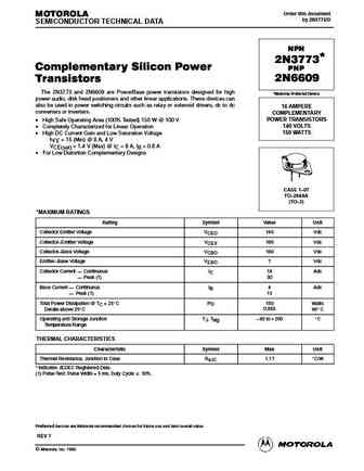
Order this document MOTOROLA by 2N3773/D SEMICONDUCTOR TECHNICAL DATA NPN 2N3773* Complementary Silicon Power PNP 2N6609 Transistors The 2N3773 and 2N6609 are PowerBase power transistors designed for high *Motorola Preferred Device power audio, disk head positioners and other linear applications. These devices can also be used in power switching circuits such as relay or solenoid d
2n6668.pdf
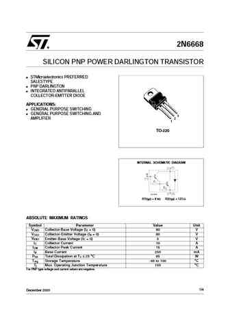
2N6668 SILICON PNP POWER DARLINGTON TRANSISTOR STMicroelectronics PREFERRED SALESTYPE PNP DARLINGTON INTEGRATED ANTIPARALLEL COLLECTOR-EMITTER DIODE APPLICATIONS GENERAL PURPOSE SWITCHING GENERAL PURPOSE SWITCHING AND 3 AMPLIFIER 2 1 TO-220 INTERNAL SCHEMATIC DIAGRAM R1(typ) = 8 k R2(typ) = 120 ABSOLUTE MAXIMUM RATINGS Symbol Parameter Value Unit VCBO Col
2n6661-2.pdf

2N6661, 2N6661-2, 2N6661JANTX, 2N6661JANTXV www.vishay.com Vishay Siliconix N-Channel 90 V (D-S) MOSFET FEATURES PRODUCT SUMMARY Military Qualified VDS (V) 90 Low On-Resistence 3.6 RDS(on) ( ) at VGS = 10 V 4 Low Threshold 1.6 V Configuration Single Low Input Capacitance 35 pF Fast Switching Speed 6 ns TO-205AD Low Input and Output Leakage (TO-39
2n6660-2.pdf
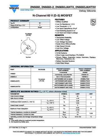
2N6660, 2N6660-2, 2N6660JANTX, 2N6660JANTXV www.vishay.com Vishay Siliconix N-Channel 60 V (D-S) MOSFET FEATURES PRODUCT SUMMARY Military Qualified VDS (V) 60 Low On-Resistence 1.3 RDS(on) ( ) at VGS = 10 V 3 Low Threshold 1.7 V Configuration Single Low Input Capacitance 35 pF Fast Switching Speed 8 ns Low Input and Output Leakage TO-205AD (TO-3
2n6661 vn88afd.pdf
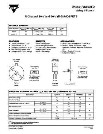
2N6661/VN88AFD Vishay Siliconix N-Channel 80-V and 90-V (D-S) MOSFETS PRODUCT SUMMARY Part Number V(BR)DSS Min (V) rDS(on) Max (W) VGS(th) (V) ID (A) 2N6661 90 4 @ VGS = 10 V 0.8 to 2 0.9 VN88AFD 80 4 @ VGS = 10 V 0.8 to 2.5 1.29 FEATURES BENEFITS APPLICATIONS D Low On-Resistance 3.6 W D Low Offset Voltage D Direct Logic-Level Interface TTL/CMOS D Low Threshold 1.6 V D Low-Voltage O
2n6659-2.pdf
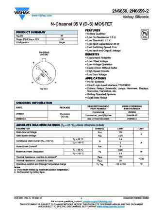
2N6659, 2N6659-2 www.vishay.com Vishay Siliconix N-Channel 35 V (D-S) MOSFET FEATURES PRODUCT SUMMARY Military Qualified VDS (V) 35 Low On-Resistence 1.3 RDS(on) ( ) at VGS = 10 V 1.8 Low Threshold 1.7 V Configuration Single Low Input Capacitance 35 pF Fast Switching Speed 8 ns Low Input and Output Leakage TO-205AD BENEFITS (TO-39) Guarant
2n3773 2n6609.pdf
TM Central Semiconductor Corp. 145 Adams Avenue Hauppauge, NY 11788 USA Tel (631) 435-1110 Fax (631) 435-1824 www.centralsemi.com
2n3773 2n6609.pdf
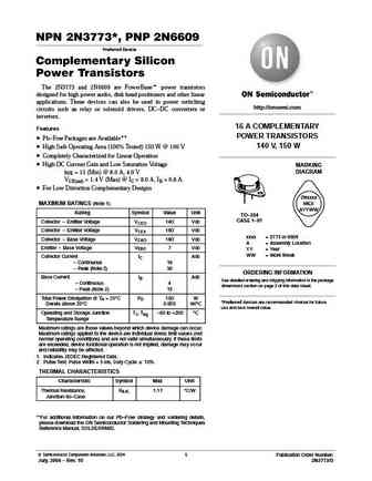
NPN 2N3773*, PNP 2N6609 Preferred Device Complementary Silicon Power Transistors The 2N3773 and 2N6609 are PowerBaset power transistors designed for high power audio, disk head positioners and other linear applications. These devices can also be used in power switching http //onsemi.com circuits such as relay or solenoid drivers, DC-DC converters or inverters. 16 A COMPLEMENTARY Feat
2n6661.pdf
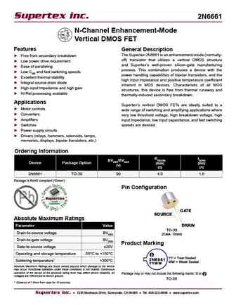
Supertex inc. 2N6661 N-Channel Enhancement-Mode Vertical DMOS FET Features General Description The Supertex 2N6661 is an enhancement-mode (normally- Free from secondary breakdown off) transistor that utilizes a vertical DMOS structure Low power drive requirement and Supertex s well-proven silicon-gate manufacturing Ease of paralleling process. This combination produc
2n6660.pdf
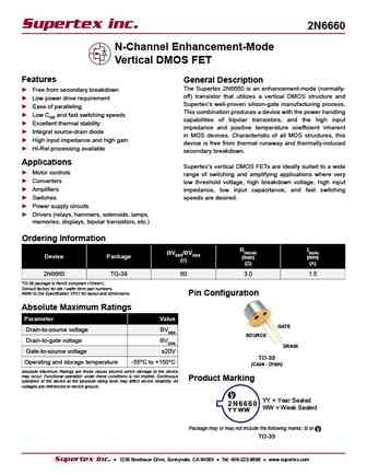
Supertex inc. 2N6660 N-Channel Enhancement-Mode Vertical DMOS FET Features General Description The Supertex 2N6660 is an enhancement-mode (normally- Free from secondary breakdown off) transistor that utilizes a vertical DMOS structure and Low power drive requirement Supertex s well-proven silicon-gate manufacturing process. Ease of paralleling This combination produ
2n6660 2n6661.pdf
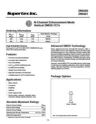
2N6660 2N6661 N-Channel Enhancement-Mode Vertical DMOS FETs Ordering Information Order Number / Package BVDSS /RDS(ON) ID(ON) BVDGS (max) (min) TO-39 60V 3.0 1.5A 2N6660 90V 4.0 1.5A 2N6661 High Reliability Devices Advanced DMOS Technology See pages 5-4 and 5-5 for MILITARY STANDARD Process These enhancement-mode (normally-off) transistors utilize a Flows and Ordering Informa
2n6676-t1-t3 2n6678-t1-t3 2n6691 2n6693.pdf
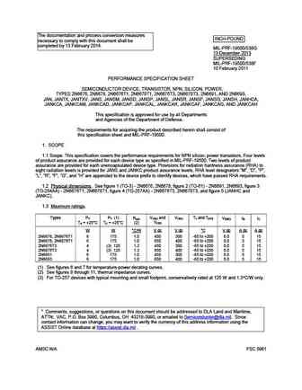
The documentation and process conversion measures INCH-POUND necessary to comply with this document shall be completed by 13 February 2014. MIL-PRF-19500/538G 13 December 2013 SUPERSEDING MIL-PRF-19500/538F 10 February 2011 PERFORMANCE SPECIFICATION SHEET SEMICONDUCTOR DEVICE, TRANSISTOR, NPN, SILICON, POWER, TYPES 2N6676, 2N6678, 2N6676T1, 2N6678T1, 2N6676T3, 2N6678T3, 2
2n6661m1a.pdf
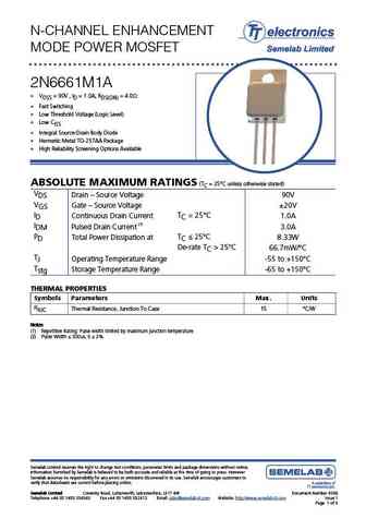
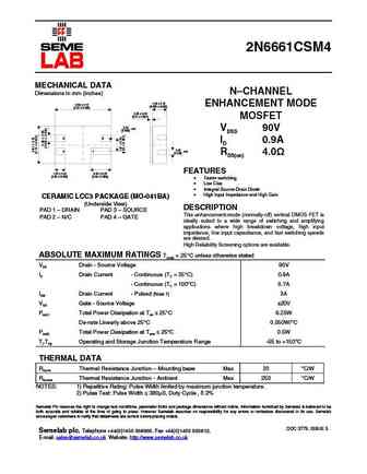
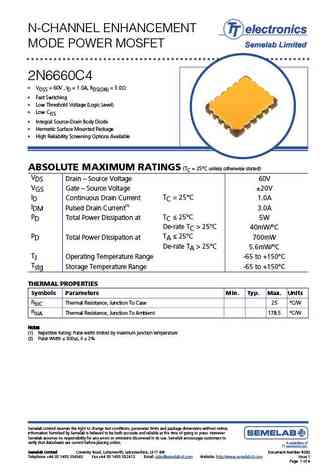
N-CHANNEL ENHANCEMENT MODE POWER MOSFET 2N6661M1A VDSS = 90V , ID = 1.0A, RDS(ON) = 4.0 Fast Switching Low Threshold Voltage (Logic Level) Low CISS Integral Source-Drain Body Diode Hermetic Metal TO-257AA Package High Reliability Screening Options Available ABSOLUTE MAXIMUM RATINGS (TC = 25 C unless otherwise stated) VDS Drain Source V
2n6659x.pdf
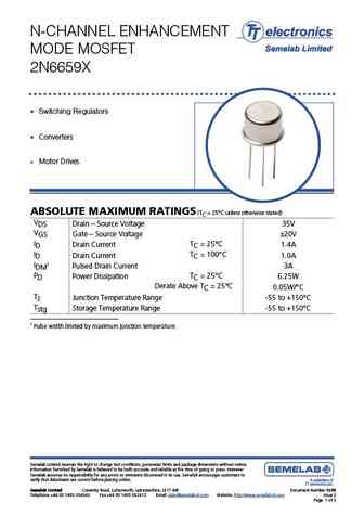
N-CHANNEL ENHANCEMENT MODE MOSFET 2N6659X Switching Regulators Converters Motor Drives ABSOLUTE MAXIMUM RATINGS (TC = 25 C unless otherwise stated) VDS Drain Source Voltage 35V VGS Gate Source Voltage 20V ID TC = 25 C Drain Current 1.4A ID TC = 100 C Drain Current 1.0A IDM1 Pulsed Drain Current 3A PD TC = 25 C Power Dissipation 6.25W
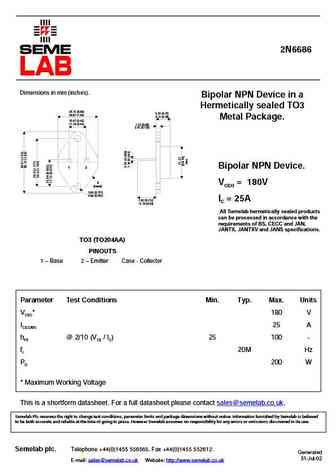
2n6687.pdf
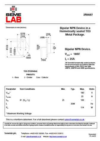
2N6687 Dimensions in mm (inches). Bipolar NPN Device in a Hermetically sealed TO3 25.15 (0.99) 6.35 (0.25) 26.67 (1.05) 9.15 (0.36) Metal Package. 10.67 (0.42) 11.18 (0.44) 1.52 (0.06) 3.43 (0.135) 1 2 Bipolar NPN Device. 3 VCEO = 180V (case) 3.84 (0.151) 4.09 (0.161) 7.92 (0.312) IC = 25A 12.70 (0.50) All Semelab hermetically sealed products can be processed in
2n6653.pdf

2N6653 Dimensions in mm (inches). Bipolar NPN Device in a Hermetically sealed TO3 25.15 (0.99) 6.35 (0.25) 26.67 (1.05) 9.15 (0.36) Metal Package. 10.67 (0.42) 11.18 (0.44) 1.52 (0.06) 3.43 (0.135) 1 2 Bipolar NPN Device. 3 VCEO = 300V (case) 3.84 (0.151) 4.09 (0.161) 7.92 (0.312) IC = 20A 12.70 (0.50) All Semelab hermetically sealed products can be processed in
2n6678m3a.pdf
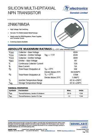
SILICON MULTI-EPITAXIAL NPN TRANSISTOR 2N6678M3A High Voltage, Fast Switching. Hermetic TO-254AA Isolated Metal Package. Ideally suited for PWM Regulators, Power Supplies and Converter Circuits Screening Options Available ABSOLUTE MAXIMUM RATINGS (TC = 25 C unless otherwise stated) VCBO Collector Base Voltage 650V VCEX VBE = -1.5V Collector Emitt
2n6654.pdf

2N6654 Dimensions in mm (inches). Bipolar NPN Device in a Hermetically sealed TO3 25.15 (0.99) 6.35 (0.25) 26.67 (1.05) 9.15 (0.36) Metal Package. 10.67 (0.42) 11.18 (0.44) 1.52 (0.06) 3.43 (0.135) 1 2 Bipolar NPN Device. 3 VCEO = 350V (case) 3.84 (0.151) 4.09 (0.161) 7.92 (0.312) IC = 20A 12.70 (0.50) All Semelab hermetically sealed products can be processed in
2n6686.pdf
2N6686 Dimensions in mm (inches). Bipolar NPN Device in a Hermetically sealed TO3 25.15 (0.99) 6.35 (0.25) 26.67 (1.05) 9.15 (0.36) Metal Package. 10.67 (0.42) 11.18 (0.44) 1.52 (0.06) 3.43 (0.135) 1 2 Bipolar NPN Device. 3 VCEO = 180V (case) 3.84 (0.151) 4.09 (0.161) 7.92 (0.312) IC = 25A 12.70 (0.50) All Semelab hermetically sealed products can be processed in
2n6660csm4.pdf
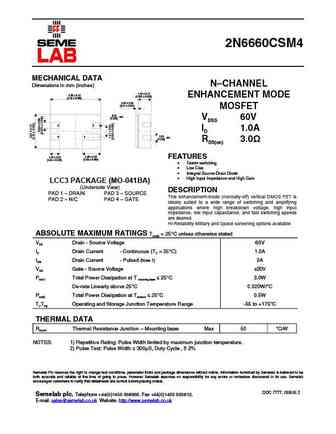
2N6660CSM4 MECHANICAL DATA N CHANNEL Dimensions in mm (inches) 1.40 0.15 5.59 0.13 (0.055 0.006) ENHANCEMENT MODE (0.22 0.005) 0.25 0.03 (0.01 0.001) MOSFET 0.23 rad. (0.009) V 60V DSS 3 2 I 1.0A D 0.23 4 1 min. (0.009) R 3.0 DS(on) 1.02 0.20 2.03 0.20 FEATURES (0.04 0.008) (0.08 0.008) Faster switching Low Ciss
2n6659.pdf
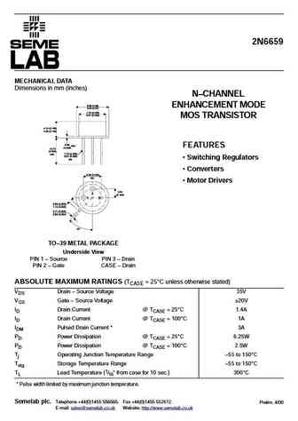
2N6659 MECHANICAL DATA Dimensions in mm (inches) N CHANNEL 8.89 (0.35) ENHANCEMENT MODE 9.40 (0.37) 7.75 (0.305) 8.51 (0.335) MOS TRANSISTOR 4.19 (0.165) 4.95 (0.195) 0.89 max. FEATURES (0.035) 12.70 (0.500) 7.75 (0.305) min. 8.51 (0.335) Switching Regulators dia. Converters 5.08 (0.200) typ. Motor Drivers 2.54 2 (0.100) 1 3 0.66 (0.026) 1.14 (0.045
2n6661csm4.pdf
2N6661CSM4 MECHANICAL DATA N CHANNEL Dimensions in mm (inches) 1.40 0.15 5.59 0.13 ENHANCEMENT MODE (0.055 0.006) (0.22 0.005) 0.25 0.03 (0.01 0.001) MOSFET 0.23 rad. V 90V (0.009) DSS 3 2 I 0.9A D 0.23 4 1 min. (0.009) R 4.0 DS(on) FEATURES 1.02 0.20 2.03 0.20 (0.04 0.008) (0.08 0.008) Faster switching Low Ciss
2n6661dcsm.pdf
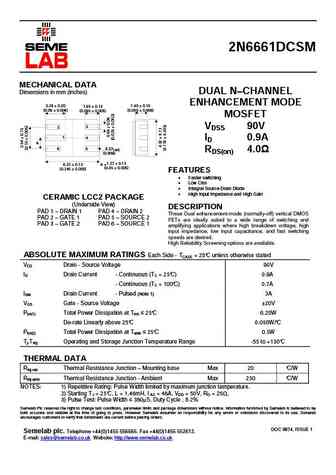
2N6661DCSM MECHANICAL DATA DUAL N CHANNEL Dimensions in mm (inches) ENHANCEMENT MODE 1.40 0.15 2.29 0.20 1.65 0.13 (0.055 0.006) (0.09 0.008) (0.065 0.005) MOSFET 2 3 VDSS 90V 1 4 ID 0.9A A 0.23 6 5 rad. RDS(on) 4.0 (0.009) 6.22 0.13 A = 1.27 0.13 (0.05 0.005) (0.245 0.005) FEATURES Faster switching Low Ciss In
2n6655.pdf
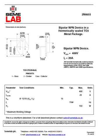
2N6655 Dimensions in mm (inches). Bipolar NPN Device in a Hermetically sealed TO3 25.15 (0.99) 6.35 (0.25) 26.67 (1.05) 9.15 (0.36) Metal Package. 10.67 (0.42) 11.18 (0.44) 1.52 (0.06) 3.43 (0.135) 1 2 Bipolar NPN Device. 3 VCEO = 400V (case) 3.84 (0.151) 4.09 (0.161) 7.92 (0.312) IC = 20A 12.70 (0.50) All Semelab hermetically sealed products can be processed in
2n6660c4a.pdf
N-CHANNEL ENHANCEMENT MODE POWER MOSFET 2N6660C4 VDSS = 60V , ID = 1.0A, RDS(ON) = 3.0 Fast Switching Low Threshold Voltage (Logic Level) Low CISS Integral Source-Drain Body Diode Hermetic Surface Mounted Package High Reliability Screening Options Available ABSOLUTE MAXIMUM RATINGS (TC = 25 C unless otherwise stated) VDS Drain Source V
2n6666 2n6667 2n6668.pdf
A B O C A S E M I C O N D U C T O R C O R P A Boca Semiconductor Corp. BSC http //www.bocasemi.com A Boca Semiconductor Corp. BSC http //www.bocasemi.com
2n6653.pdf

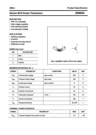
JMnic Product Specification Silicon NPN Power Transistors 2N6653 DESCRIPTION With TO-3 package High voltage capability Fast switching speeds Low saturation voltage APPLICATIONS Switcing regulators Inverters Solenoid and relay drivers Deflection circuits PINNING (See Fig.2) PIN DESCRIPTION 1 Base 2 Emitter Fig.1 simplified outline (TO-3) and symbol
2n6654.pdf
JMnic Product Specification Silicon NPN Power Transistors 2N6654 DESCRIPTION With TO-3 package High voltage capability Fast switching speeds Low saturation voltage APPLICATIONS Switcing regulators Inverters Solenoid and relay drivers Deflection circuits PINNING (See Fig.2) PIN DESCRIPTION 1 Base 2 Emitter Fig.1 simplified outline (TO-3) and symbol
2n6674.pdf
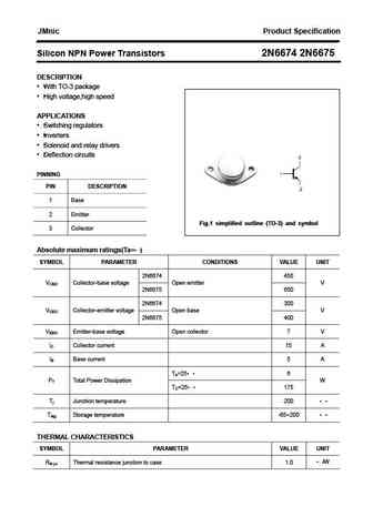
JMnic Product Specification Silicon NPN Power Transistors 2N6674 2N6675 DESCRIPTION With TO-3 package High voltage,high speed APPLICATIONS Switching regulators Inverters Solenoid and relay drivers Deflection circuits PINNING PIN DESCRIPTION 1 Base 2 Emitter Fig.1 simplified outline (TO-3) and symbol 3 Collector Absolute maximum ratings(Ta= ) SYMBOL P
2n6671 2n6672 2n6673.pdf
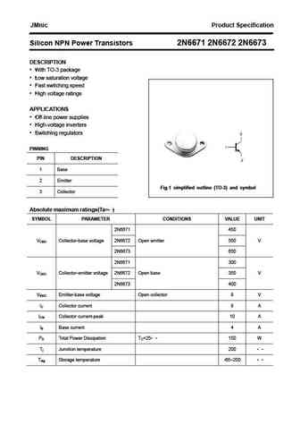
JMnic Product Specification Silicon NPN Power Transistors 2N6671 2N6672 2N6673 DESCRIPTION With TO-3 package Low saturation voltage Fast switching speed High voltage ratings APPLICATIONS Off-line power supplies High-voltage inverters Switching regulators PINNING PIN DESCRIPTION 1 Base 2 Emitter Fig.1 simplified outline (TO-3) and symbol 3 Collector A
2n6674 2n6675 2n6689 2n6690.pdf

TECHNICAL DATA NPN POWER SILICON TRANSISTOR Qualified per MIL-PRF-19500/537 Devices Qualified Level JAN 2N6674 2N6675 2N6689 2N6690 JANTX JANTXV MAXIMUM RATINGS Ratings Symbol 2N6674 2N6675 Unit 2N6689 2N6690 Collector-Emitter Voltage 300 400 Vdc VCEO Collector-Base Voltage 450 650 Vdc VCBO Collector-Base Voltage 450 650 Vdc VCEX Emitter-Base Voltage 7.0 Vdc VE
2n6676 2n6678 2n6691 2n6693.pdf
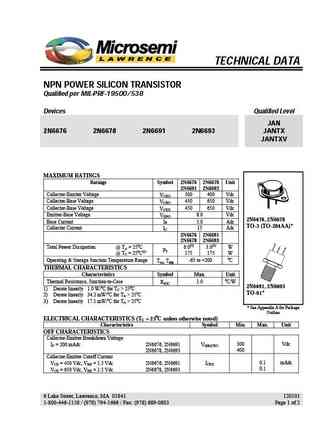
TECHNICAL DATA NPN POWER SILICON TRANSISTOR Qualified per MIL-PRF-19500/538 Devices Qualified Level JAN 2N6676 2N6678 2N6691 2N6693 JANTX JANTXV MAXIMUM RATINGS Ratings Symbol 2N6676 2N6678 Unit 2N6691 2N6693 Collector-Emitter Voltage 300 400 Vdc VCEO Collector-Base Voltage 450 650 Vdc VCBO Collector-Base Voltage 450 650 Vdc VCEX Emitter-Base Voltage 8.0 Vdc VE
2n6676 2n6678.pdf
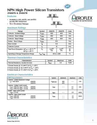
NPN High Power Silicon Transistors 2N6676 & 2N6678 Features Available in JAN, JANTX, and JANTXV per MIL-PRF-19500/538 TO-3 (TO-204AA) Package Maximum Ratings Ratings Symbol 2N6676 2N6678 Units Collector - Emitter Voltage VCEO 300 400 Vdc Collector - Base Voltage VCBO 450 650 Vdc Collector - Base Voltage VCBX 450 650 Vdc Emitter - Base Voltage VEBO 8.0 Vdc Base Current IB 5.
2n6674 2n6675.pdf
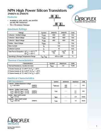
NPN High Power Silicon Transistors 2N6674 & 2N6675 Features Available in JAN, JANTX, and JANTXV per MIL-PRF-19500/537 TO-3 (TO-204AA) Package Maximum Ratings Ratings Symbol 2N6674 2N6675 Units Collector - Emitter Voltage VCEO 300 400 Vdc Collector - Base Voltage VCBO 450 650 Vdc Collector - Base Voltage VCBX 450 650 Vdc Emitter - Base Voltage VEBO 7.0 Vdc Base Current IB 5.
2n6678.pdf
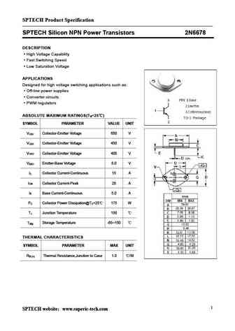
SPTECH Product Specification SPTECH Silicon NPN Power Transistors 2N6678 DESCRIPTION High Voltage Capability Fast Switching Speed Low Saturation Voltage APPLICATIONS Designed for high voltage switching applications such as Off-line power supplies Converter circuits PWM regulators ABSOLUTE MAXIMUM RATINGS(T =25 ) a SYMBOL PARAMETER VALUE UNIT V Collector-Emitter Volt
2n6678.pdf
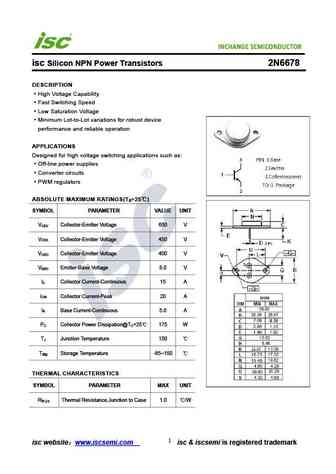
INCHANGE Semiconductor isc Silicon NPN Power Transistors 2N6678 DESCRIPTION High Voltage Capability Fast Switching Speed Low Saturation Voltage Minimum Lot-to-Lot variations for robust device performance and reliable operation APPLICATIONS Designed for high voltage switching applications such as Off-line power supplies Converter circuits PWM regulators ABSOLUTE MAXIM
2n6648.pdf
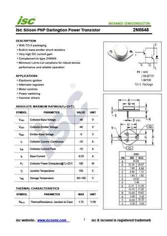
isc Product Specification isc Silicon PNP Darlingtion Power Transistor 2N6648 DESCRIPTION With TO-3 packaging Built-in base-emitter shunt resistors Very high DC current gain Complement to type 2N6648 Minimum Lot-to-Lot variations for robust device performance and reliable operation APPLICATIONS Electronic ignition Alternator regulator Motor controls Power switchin
2n6687.pdf
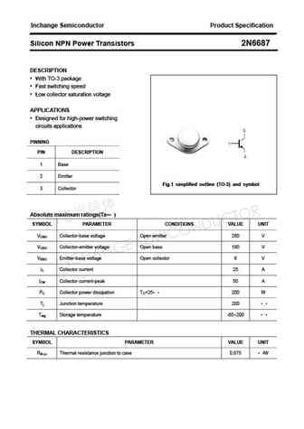
Inchange Semiconductor Product Specification Silicon NPN Power Transistors 2N6687 DESCRIPTION With TO-3 package Fast switching speed Low collector saturation voltage APPLICATIONS Designed for high-power switching circuits applications PINNING PIN DESCRIPTION 1 Base 2 Emitter Fig.1 simplified outline (TO-3) and symbol 3 Collector Absolute maximum ratings(Ta=
2n6653.pdf

isc Silicon NPN Power Transistor 2N6653 DESCRIPTION High Voltage Capability High Current Current Capability Low Collector Saturation Voltage- High Switching Speed Minimum Lot-to-Lot variations for robust device performance and reliable operation APPLICATIONS Desinged for use in switching and linear applications in military and power conversion. Absolute maximum ratings(Ta
2n6654.pdf
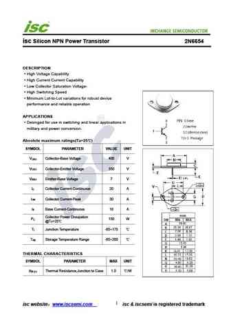
isc Silicon NPN Power Transistor 2N6654 DESCRIPTION High Voltage Capability High Current Current Capability Low Collector Saturation Voltage- High Switching Speed Minimum Lot-to-Lot variations for robust device performance and reliable operation APPLICATIONS Desinged for use in switching and linear applications in military and power conversion. Absolute maximum ratings(Ta
2n6686.pdf
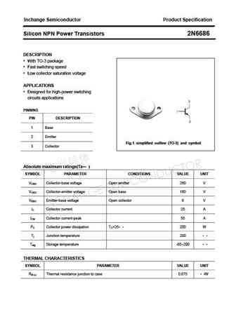
Inchange Semiconductor Product Specification Silicon NPN Power Transistors 2N6686 DESCRIPTION With TO-3 package Fast switching speed Low collector saturation voltage APPLICATIONS Designed for high-power switching circuits applications PINNING PIN DESCRIPTION 1 Base 2 Emitter Fig.1 simplified outline (TO-3) and symbol 3 Collector Absolute maximum ratings(Ta=
2n6676 2n6677 2n6678.pdf
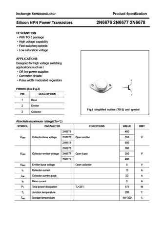
Inchange Semiconductor Product Specification Silicon NPN Power Transistors 2N6676 2N6677 2N6678 DESCRIPTION With TO-3 package High voltage capability Fast switching speeds Low saturation voltage APPLICATIONS Designed for high voltage switching applications such as Off-line power supplies Converter circuits Pulse width modulated regulators PINNING (See F
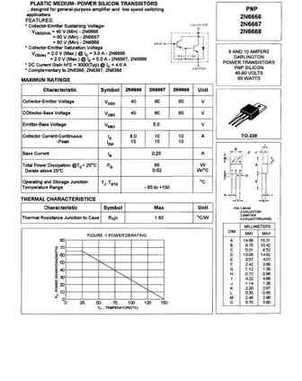
2n6666.pdf
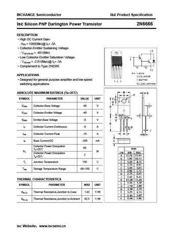
INCHANGE Semiconductor isc Product Specification isc Silicon PNP Darlington Power Transistor 2N6666 DESCRIPTION High DC Current Gain- hFE = 1000(Min)@ IC= -3A Collector-Emitter Sustaining Voltage- VCEO(SUS) = -40V(Min) Low Collector-Emitter Saturation Voltage- VCE(sat) = -2.0V(Max)@ IC= -3A Complement to Type 2N6386 APPLICATIONS Designed for general purpo
2n6671 2n6672 2n6673.pdf
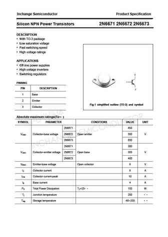
Inchange Semiconductor Product Specification Silicon NPN Power Transistors 2N6671 2N6672 2N6673 DESCRIPTION With TO-3 package Low saturation voltage Fast switching speed High voltage ratings APPLICATIONS Off-line power supplies High-voltage inverters Switching regulators PINNING PIN DESCRIPTION 1 Base 2 Emitter Fig.1 simplified outline (TO-3) and symbol
2n6688.pdf

Inchange Semiconductor Product Specification Silicon NPN Power Transistors 2N6688 DESCRIPTION With TO-3 package Fast switching speed Low collector saturation voltage APPLICATIONS Designed for high-power switching circuits applications PINNING PIN DESCRIPTION 1 Base 2 Emitter Fig.1 simplified outline (TO-3) and symbol 3 Collector Absolute maximum ratings(Ta=
2n6674 2n6675.pdf
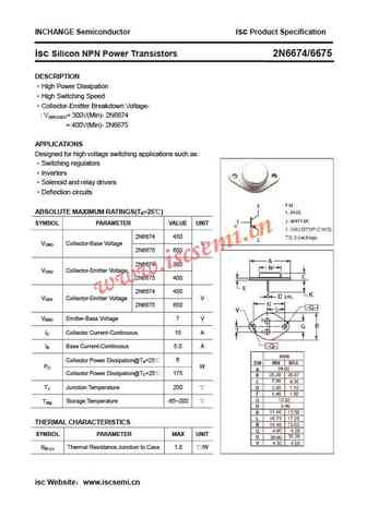
INCHANGE Semiconductor isc Product Specification isc Silicon NPN Power Transistors 2N6674/6675 DESCRIPTION High Power Dissipation High Switching Speed Collector-Emitter Breakdown Voltage- V(BR)CEO= 300V(Min)- 2N6674 = 400V(Min)- 2N6675 APPLICATIONS Designed for high voltage switching applications such as Switching regulators Inverters Solenoid and relay d
Другие транзисторы: 2N6592, 2N6593, 2N6594, 2N6595, 2N6596, 2N6597, 2N6598, 2N6599, B647, 2N660, 2N6600, 2N6601, 2N6602, 2N6603, 2N6604, 2N6609, 2N661
Параметры биполярного транзистора и их взаимосвязь
History: MD7021 | AFY39
🌐 : EN
ES
РУ

Список транзисторов
Обновления
BJT: GA1A4M | SBT42 | 2SA200-Y | 2SA200-O | 2SD882-Q | 2SD882-P | 2SD882-E | 2SC945-L | 2SC945-H | 2SC4226-R23 | 2SC3357-F | 2SC3357-E | 2SC3356-R26 | 2SC3356-R24 | 2SC3356-R23 | 2SB772-Q | 2SB772-P | 2SB772-E | 2SA1015-L | 2SA1015-H | HSS8550
Popular searches
bc546 datasheet | mpsa06 transistor | tta004b | 2sc1116 | 2n3565 equivalent | 10n60 | 2sc1061 | a1023