2N21 Datasheet. Specs and Replacement
Type Designator: 2N21 📄📄
Material of Transistor: Ge
Polarity: PNP
Absolute Maximum Ratings
Maximum Collector Power Dissipation (Pc): 0.12 W
Maximum Collector-Base Voltage |Vcb|: 100 V
Maximum Collector-Emitter Voltage |Vce|: 100 V
Maximum Collector Current |Ic max|: 0.04 A
Max. Operating Junction Temperature (Tj): 85 °C
Electrical Characteristics
Transition Frequency (ft): 1 MHz
Forward Current Transfer Ratio (hFE), MIN: 35
Noise Figure, dB: -
Package: TO22
- BJT ⓘ Cross-Reference Search
2N21 datasheet
0.8. Size:45K st
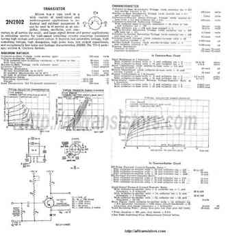
2n2102.pdf 
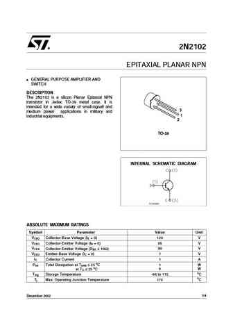
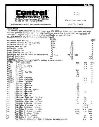
2N2102 EPITAXIAL PLANAR NPN GENERAL PURPOSE AMPLIFIER AND SWITCH DESCRIPTION The 2N2102 is a silicon Planar Epitaxial NPN transistor in Jedec TO-39 metal case. It is intended for a wide variety of small-signall and medium power applications in military and industrial equipments. TO-39 INTERNAL SCHEMATIC DIAGRAM ABSOLUTE MAXIMUM RATINGS Symbol Parameter Value Unit VCBO Collec... See More ⇒
0.9. Size:47K st
2n2102 .pdf

2N2102 EPITAXIAL PLANAR NPN GENERAL PURPOSE AMPLIFIER AND SWITCH DESCRIPTION The 2N2102 is a silicon Planar Epitaxial NPN transistor in Jedec TO-39 metal case. It is intended for a wide variety of small-signall and medium power applications in military and industrial equipments. TO-39 INTERNAL SCHEMATIC DIAGRAM ABSOLUTE MAXIMUM RATINGS Symbol Parameter Value Unit VCBO Collec... See More ⇒
0.10. Size:74K central
2n2102-a.pdf
145 Adams Avenue, Hauppauge, NY 11788 USA Tel (631) 435-1110 Fax (631) 435-1824 ... See More ⇒
0.11. Size:141K ixys
de475-102n21a.pdf
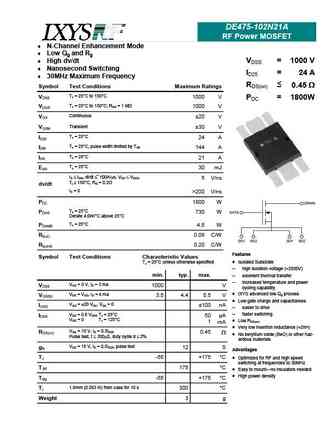
DE475-102N21A RF Power MOSFET N-Channel Enhancement Mode Low Qg and Rg High dv/dt VDSS = 1000 V Nanosecond Switching ID25 = 24 A 30MHz Maximum Frequency RDS(on) Symbol Test Conditions Maximum Ratings 0.45 TJ = 25 C to 150 C VDSS 1000 V PDC = 1800W TJ = 25 C to 150 C; RGS = 1 M VDGR 1000 V Continuous VGS 20 V T... See More ⇒
0.12. Size:11K semelab
2n2102.pdf
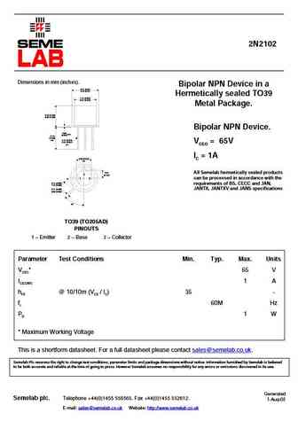
2N2102 Dimensions in mm (inches). Bipolar NPN Device in a 8.51 (0.34) 9.40 (0.37) Hermetically sealed TO39 7.75 (0.305) 8.51 (0.335) Metal Package. 6.10 (0.240) 6.60 (0.260) Bipolar NPN Device. 0.89 max. (0.035) 12.70 (0.500) min. 0.41 (0.016) 0.53 (0.021) VCEO = 65V dia. IC = 1A 5.08 (0.200) typ. 2.54 All Semelab hermetically sealed products 2 (0.100) 1 3 ... See More ⇒
0.13. Size:164K isahaya
rt2n21m.pdf
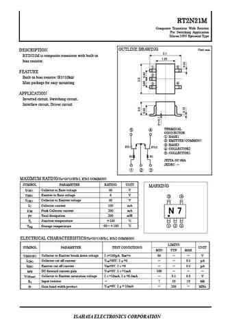
RT2N21M Composite Transistor With Resistor For Switching Application Silicon NPN Epitaxial Type OUTLINE DRAWING Unit mm DESCRIPTION 2.1 RT2N21M is composite transistor with built-in 1.25 bias resistor. FEATURE Built-in bias resistor (R1=10k ) Mini package for easy mounting APPLICATION Inverted circuit, Switching circuit, Interface circui... See More ⇒
0.14. Size:227K cdil
2n2102.pdf
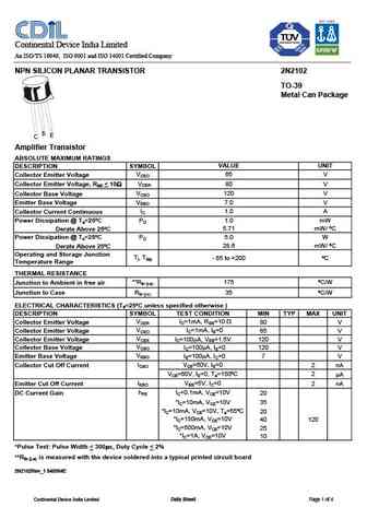
Continental Device India Limited An ISO/TS 16949, ISO 9001 and ISO 14001 Certified Company NPN SILICON PLANAR TRANSISTOR 2N2102 TO-39 Metal Can Package Amplifier Transistor ABSOLUTE MAXIMUM RATINGS DESCRIPTION SYMBOL VALUE UNIT VCEO Collector Emitter Voltage 65 V Collector Emitter Voltage, RBE ... See More ⇒
0.15. Size:65K microsemi
2n2150 2n2151.pdf
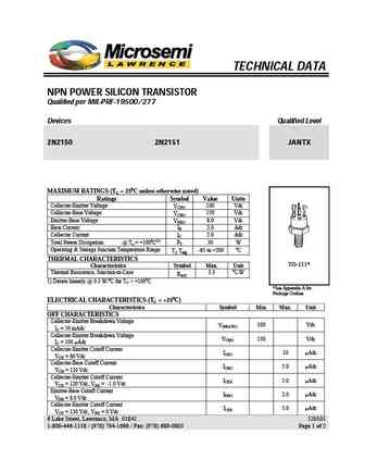
TECHNICAL DATA NPN POWER SILICON TRANSISTOR Qualified per MIL-PRF-19500/277 Devices Qualified Level 2N2150 2N2151 JANTX MAXIMUM RATINGS (TC = 250C unless otherwise noted) Ratings Symbol Value Units Collector-Emitter Voltage 100 Vdc VCEO Collector-Base Voltage 150 Vdc VCBO Emitter-Base Voltage 8.0 Vdc VEBO Base Current I 2.0 Adc B Collector Current 2.0 Adc IC To... See More ⇒
Detailed specifications: 2N2093, 2N2094, 2N2094A, 2N2095, 2N2096, 2N2097, 2N2098, 2N2099, 2SC2240, 2N2100, 2N2100A, 2N2101, 2N2102, 2N2102A, 2N2102L, 2N2102S, 2N2104
Keywords - 2N21 pdf specs
2N21 cross reference
2N21 equivalent finder
2N21 pdf lookup
2N21 substitution
2N21 replacement