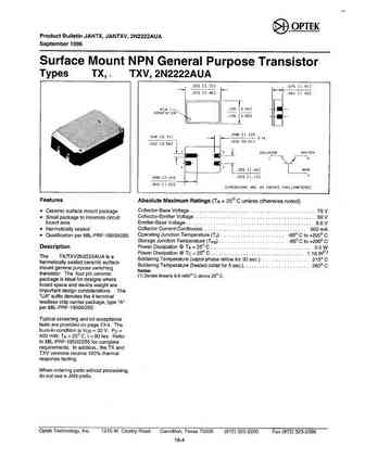
2N2222CSM Datasheet. Specs and Replacement
Type Designator: 2N2222CSM 📄📄
Material of Transistor: Si
Polarity: NPN
Absolute Maximum Ratings
Maximum Collector Power Dissipation (Pc): 0.5 W
Maximum Collector-Base Voltage |Vcb|: 75 V
Maximum Collector-Emitter Voltage |Vce|: 40 V
Maximum Emitter-Base Voltage |Veb|: 6 V
Maximum Collector Current |Ic max|: 0.8 A
Max. Operating Junction Temperature (Tj): 175 °C
Electrical Characteristics
Transition Frequency (ft): 250 MHz
Collector Capacitance (Cc): 8 pF
Forward Current Transfer Ratio (hFE), MIN: 100
Noise Figure, dB: -
Package: LCC3
📄📄 Copy
- BJT ⓘ Cross-Reference Search
2N2222CSM datasheet
8.1. Size:238K motorola
mtp2n2222a p2n2222a.pdf 

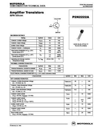
MOTOROLA Order this document SEMICONDUCTOR TECHNICAL DATA by P2N2222A/D Amplifier Transistors NPN Silicon P2N2222A COLLECTOR 1 2 BASE 3 EMITTER MAXIMUM RATINGS Rating Symbol Value Unit 1 2 Collector Emitter Voltage VCEO 40 Vdc 3 Collector Base Voltage VCBO 75 Vdc CASE 29 04, STYLE 17 Emitter Base Voltage VEBO 6.0 Vdc TO 92 (TO 226AA) Collector Current Conti... See More ⇒
8.2. Size:53K philips
2n2222 2n2222a cnv 2.pdf 

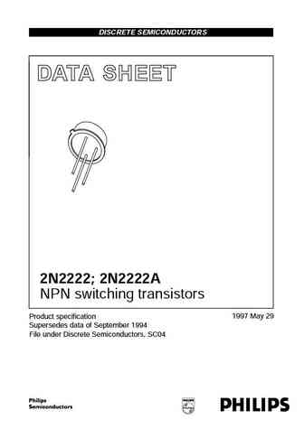
DISCRETE SEMICONDUCTORS DATA SHEET M3D125 2N2222; 2N2222A NPN switching transistors 1997 May 29 Product specification Supersedes data of September 1994 File under Discrete Semiconductors, SC04 Philips Semiconductors Product specification NPN switching transistors 2N2222; 2N2222A FEATURES PINNING High current (max. 800 mA) PIN DESCRIPTION Low voltage (max. 40 V). 1 emitte... See More ⇒
8.3. Size:1138K st
2n2222ahr.pdf 

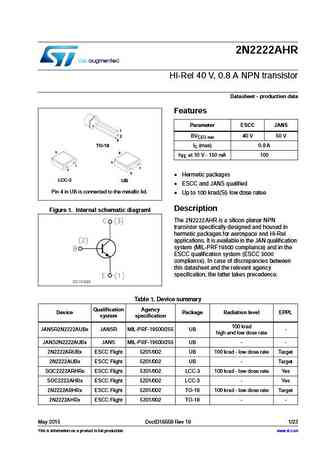
2N2222AHR Hi-Rel 40 V, 0.8 A NPN transistor Datasheet - production data Features Parameter ESCC JANS 1 2 BVCEO min 40 V 50 V 3 IC (max) 0.8 A TO-18 3 3 hFE at 10 V - 150 mA 100 4 1 1 2 2 Hermetic packages LCC-3 UB ESCC and JANS qualified Pin 4 in UB is connected to the metallic lid. Up to 100 krad(Si) low dose ratee Description Figure 1. Internal schematic ... See More ⇒
8.4. Size:166K st
2n2219a 2n2222a.pdf 

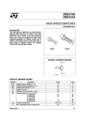
2N2219A 2N2222A HIGH SPEED SWITCHES PRELIMINARY DATA DESCRIPTION The 2N2219A and 2N2222A are silicon Planar Epitaxial NPN transistors in Jedec TO-39 (for 2N2219A) and in Jedec TO-18 (for 2N2222A) metal case. They are designed for high speed switching application at collector current up to 500mA, and feature useful current gain over a wide range of collector current, low leakage ... See More ⇒
8.5. Size:71K st
2n2218-2n2219-2n2221-2n2222.pdf 

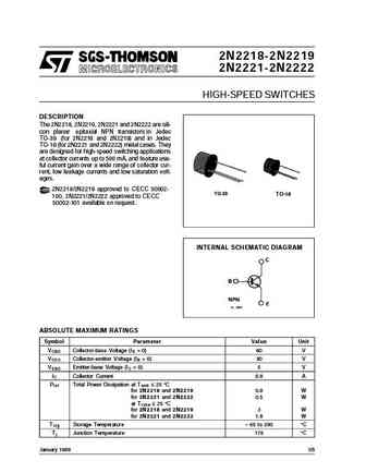
2N2218-2N2219 2N2221-2N2222 HIGH-SPEED SWITCHES DESCRIPTION The 2N2218, 2N2219, 2N2221 and 2N2222 are sili- con planar epitaxial NPN transistors in Jedec TO-39 (for 2N2218 and 2N2219) and in Jedec TO-18 (for 2N2221 and 2N2222) metal cases. They are designed for high-speed switching applications at collector currents up to 500 mA, and feature use- ful current gain over a wide range of ... See More ⇒
8.6. Size:116K central
2n2221a 2n2222a.pdf 

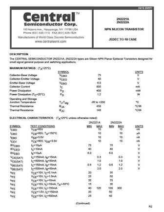
DATA SHEET 2N2221A 2N2222A NPN SILICON TRANSISTOR JEDEC TO-18 CASE DESCRIPTION The CENTRAL SEMICONDUCTOR 2N2221A, 2N2222A types are Silicon NPN Planar Epitaxial Transistors designed for small signal general purpose and switching applications. MAXIMUM RATINGS (TA=25 C) SYMBOL UNITS Collector-Base Voltage VCBO 75 V Collector-Emitter Voltage VCEO 40 V Emitter-Base Voltage ... See More ⇒
8.7. Size:232K mcc
2n2222 2n2222a to-18.pdf 

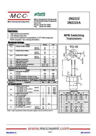
MCC 2N2222 Micro Commercial Components TM 20736 Marilla Street Chatsworth Micro Commercial Components CA 91311 2N2222A Phone (818) 701-4933 Fax (818) 701-4939 Features High current (max.800mA) Low voltage (max.40V) NPN Switching Lead Free Finish/RoHS Compliant(Note 1) ("P" Suffix designates Transistors RoHS Compliant. See ordering information) Maximum Ratings ... See More ⇒
8.8. Size:164K onsemi
p2n2222a-d.pdf 

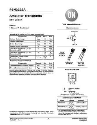
P2N2222A Amplifier Transistors NPN Silicon Features These are Pb--Free Devices* http //onsemi.com COLLECTOR 1 MAXIMUM RATINGS (TA =25 C unless otherwise noted) Characteristic Symbol Value Unit 2 BASE Collector--Emitter Voltage VCEO 40 Vdc Collector--Base Voltage VCBO 75 Vdc 3 Emitter--Base Voltage VEBO 6.0 Vdc EMITTER Collector Current -- Continuous IC 600 mAdc Total Devi... See More ⇒
8.9. Size:165K onsemi
p2n2222ag.pdf 

P2N2222A Amplifier Transistors NPN Silicon Features These are Pb--Free Devices* http //onsemi.com COLLECTOR 1 MAXIMUM RATINGS (TA =25 C unless otherwise noted) Characteristic Symbol Value Unit 2 BASE Collector--Emitter Voltage VCEO 40 Vdc Collector--Base Voltage VCBO 75 Vdc 3 Emitter--Base Voltage VEBO 6.0 Vdc EMITTER Collector Current -- Continuous IC 600 mAdc Total Devi... See More ⇒
8.11. Size:250K optek
2n2222aub.pdf 

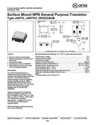
Product Bulletin JANTX, JANTXV, 2N2222AUB September 1996 Surface Mount NPN General Purpose Transistor Type JANTX, JANTXV, 2N2222AUB Feature Absolute Maximum Ratings (TA = 25o C unless otherwise noted) Collector-Base Voltage . . . . . . . . . . . . . . . . . . . . . . . . . . . . . . . . . . . . . . . . . . . . . 75 V Ceramic surface mount package Collector-Emitter Voltage. . . . . . .... See More ⇒
8.12. Size:563K semelab
2n2222ac1a.pdf 

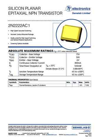
SILICON PLANAR EPITAXIAL NPN TRANSISTOR 2N2222AC1 High Speed Saturated Switching Hermetic Surface Mounted Package. Ideally suited for High Speed Switching and General Purpose Applications Screening Options Available ABSOLUTE MAXIMUM RATINGS (TA = 25 C unless otherwise stated) VCBO Collector Base Voltage 75V VCEO Collector Emitter Voltage 50V VE... See More ⇒
8.13. Size:86K semelab
2n2222ac3a 2n2222ac3b 2n2222ac3c.pdf 

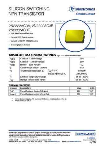
SILICON SWITCHING NPN TRANSISTOR 2N2222AC3A, 2N2222AC3B 2N2222AC3C High Speed Saturated Switching Hermetic LCC3 Ceramic package. Variant B to MIL-PRF-19500/255 outline Screening Options Available ABSOLUTE MAXIMUM RATINGS (TA = 25 C unless otherwise stated) VCBO Collector Base Voltage 75V VCEO Collector Emitter Voltage 50V VEBO Emitter Bas... See More ⇒
8.14. Size:563K semelab
2n2222ac1b.pdf 

SILICON PLANAR EPITAXIAL NPN TRANSISTOR 2N2222AC1 High Speed Saturated Switching Hermetic Surface Mounted Package. Ideally suited for High Speed Switching and General Purpose Applications Screening Options Available ABSOLUTE MAXIMUM RATINGS (TA = 25 C unless otherwise stated) VCBO Collector Base Voltage 75V VCEO Collector Emitter Voltage 50V VE... See More ⇒
8.15. Size:240K cdil
p2n2222 a.pdf 

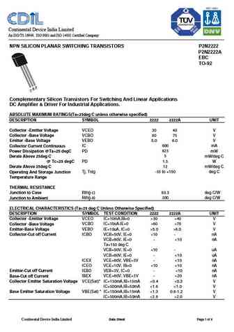
Continental Device India Limited An ISO/TS 16949, ISO 9001 and ISO 14001 Certified Company NPN SILICON PLANAR SWITCHING TRANSISTORS P2N2222 P2N2222A EBC TO-92 Complementary Silicon Transistors For Switching And Linear Applications DC Amplifier & Driver For Industrial Applications. ABSOLUTE MAXIMUM RATINGS(Ta=25deg C unless otherwise specified) DESCRIPTION SYMBOL 2222 2222A UNIT Colle... See More ⇒
8.16. Size:138K microsemi
2n2222aubc.pdf 

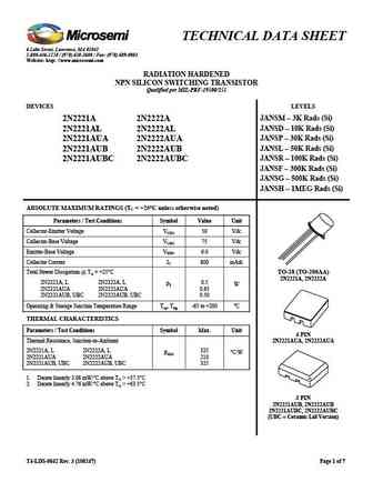
TECHNICAL DATA SHEET 6 Lake Street, Lawrence, MA 01841 1-800-446-1158 / (978) 620-2600 / Fax (978) 689-0803 Website http //www.microsemi.com RADIATION HARDENED NPN SILICON SWITCHING TRANSISTOR Qualified per MIL-PRF-19500/255 DEVICES LEVELS JANSM 3K Rads (Si) 2N2221A 2N2222A JANSD 10K Rads (Si) 2N2221AL 2N2222AL JANSP 30K Rads (Si) 2N2221AUA 2N2222AUA ... See More ⇒
8.18. Size:239K semtech
2n2222 2n2222a.pdf 

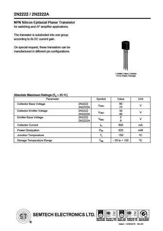
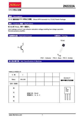
2N2222 / 2N2222A NPN Silicon Epitaxial Planar Transistor for switching and AF amplifier applications. The transistor is subdivided into one group according to its DC current gain. On special request, these transistors can be manufactured in different pin configurations. 1. Emitter 2. Base 3. Collector TO-92 Plastic Package O Absolute Maximum Ratings (Ta = 25 C) Parameter Sy... See More ⇒
8.19. Size:462K first silicon
2n2222ae.pdf 

SEMICONDUCTOR 2N2222AE TECHNICAL DATA General Purpose Transistor NPN Silicon These transistors are designed for general purpose amplifier 3 applications. They are housed in the SC-89 package which is designed for low power surface mount applications. 1 Features 2 compliance with RoHS requirements. We declare that the material of product SC-89 ORDERING INFORMATION COLLECTOR ... See More ⇒
8.20. Size:446K first silicon
2n2222as.pdf 
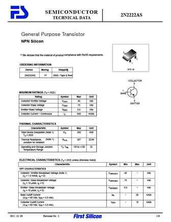
SEMICONDUCTOR 2N2222AS TECHNICAL DATA General Purpose Transistor NPN Silicon 3 compliance with RoHS requirements. We declare that the material of product 2 1 ORDERING INFORMATION SOT 23 Device Maring Shipping 2N2222AS 1P 3000 / Tape & Reel COLLECTOR 3 1 MAXIMUM RATINGS (TA = 25 C) BASE Rating Symbol Max Unit 2 Collector-Emitter Voltage VCEO 40 Vdc EMITTER Col... See More ⇒
8.21. Size:326K first silicon
2n2222au.pdf 
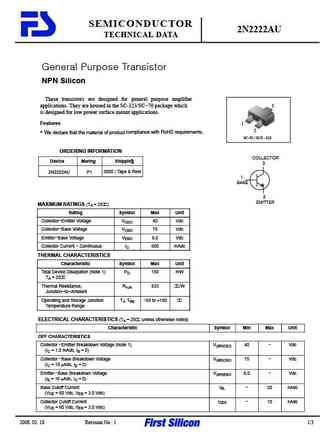
SEMICONDUCTOR 2N2222AU TECHNICAL DATA General Purpose Transistor NPN Silicon These transistors are designed for general purpose amplifier applications. They are housed in the SC-323/SC-70 package which 3 is designed for low power surface mount applications. Features 1 2 compliance with RoHS requirements. We declare that the material of product SC-70 / SOT 323 ORDERING INFO... See More ⇒
8.22. Size:377K aeroflex
2n2221a 2n2221al 2n2221aua 2n2221aub 2n2222a 2n2222al 2n2222aua 2n2222aub.pdf 

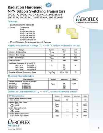
Radiation Hardened NPN Silicon Switching Transistors 2N2221A, 2N2221AL, 2N2221AUA, 2N2221AUB 2N2222A, 2N2222AL, 2N2222AUA, 2N2222AUB Features Qualified to MIL-PRF-19500/255 Levels Commerical JANS JANSM-3K Rads (Si) JANSD-l0K Rads (Si) JANSP-30K Rads (Si) JANSL-50K Rads (Si) JANSR-l00K Rads (Si) TO-18 (TO-206AA), Surface mount UA & UB Packages Absolute Maximum Ra... See More ⇒
Detailed specifications: 2N2222, 2N2222A, 2N2222ACSM, 2N2222ACSM4, 2N2222ADCSM, 2N2222AQCSM, 2N2222AQF, 2N2222AUB, 431, 2N2222DCSM, 2N2223, 2N2223A, 2N2223L, 2N2224, 2N2225, 2N2226, 2N2227
Keywords - 2N2222CSM pdf specs
2N2222CSM cross reference
2N2222CSM equivalent finder
2N2222CSM pdf lookup
2N2222CSM substitution
2N2222CSM replacement
