BD537A Datasheet. Specs and Replacement
Type Designator: BD537A 📄📄
Material of Transistor: Si
Polarity: NPN
Absolute Maximum Ratings
Maximum Collector Power Dissipation (Pc): 50 W
Maximum Collector-Base Voltage |Vcb|: 80 V
Maximum Collector-Emitter Voltage |Vce|: 80 V
Maximum Emitter-Base Voltage |Veb|: 5 V
Maximum Collector Current |Ic max|: 4 A
Max. Operating Junction Temperature (Tj): 150 °C
Electrical Characteristics
Transition Frequency (ft): 3 MHz
Forward Current Transfer Ratio (hFE), MIN: 25
Package: TO220
📄📄 Copy
BD537A Substitution
- BJT ⓘ Cross-Reference Search
BD537A datasheet
bd533 bd534 bd535 bd536 bd537.pdf ![]()
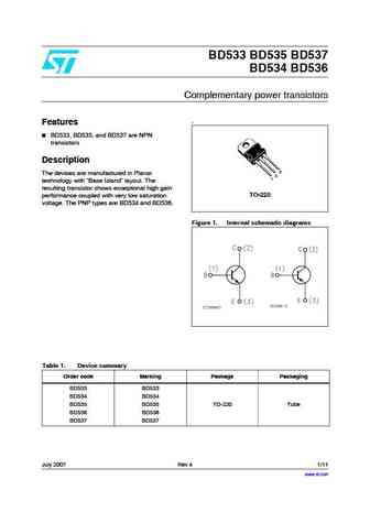
BD533 BD535 BD537 BD534 BD536 Complementary power transistors . Features BD533, BD535, and BD537 are NPN transistors Description 3 The devices are manufactured in Planar 2 1 technology with Base Island layout. The resulting transistor shows exceptional high gain TO-220 performance coupled with very low saturation voltage. The PNP types are BD534 and BD536. Figure... See More ⇒
bd533 bd534 bd535 bd536 bd537 bd538.pdf ![]()
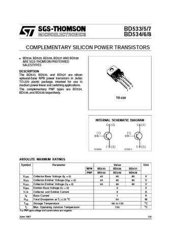
BD533/5/7 BD534/6/8 COMPLEMENTARY SILICON POWER TRANSISTORS BD534, BD535, BD536, BD537 AND BD538 ARE SGS-THOMSON PREFERRED SALESTYPES DESCRIPTION The BD533, BD535, and BD537 are silicon epitaxial-base NPN power transistors in Jedec TO-220 plastic package, intented for use in medium power linear and switching applications. 3 2 The complementary PNP types are BD534, 1 BD536, and B... See More ⇒
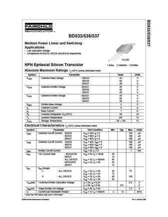
BD533/535/537 Medium Power Linear and Switching Applications Low Saturation Voltage Complement to BD534, BD536 and BD538 respectively TO-220 1 NPN Epitaxial Silicon Transistor 1.Base 2.Collector 3.Emitter Absolute Maximum Ratings TC=25 C unless otherwise noted Symbol Parameter Value Units VCBO Collector-Base Voltage BD533 45 V BD535 60 V BD537 80 V VCES Collect... See More ⇒
bd533 bd534 bd535 bd536 bd537 bd538.pdf ![]()
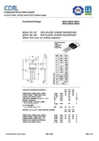
Continental Device India Limited An ISO/TS 16949, ISO 9001 and ISO 14001 Certified Company TO-220 Plastic Package BD533, BD535, BD537 BD534, BD536, BD538 BD533, 535, 537 NPN PLASTIC POWER TRANSISTORS BD534, 536, 538 PNP PLASTIC POWER TRANSISTORS Medium Power Linear and Switching Applications PIN CONFIGURATION 4 1. BASE 2. COLLECTOR 3. EMITTER 4. COLLECTOR 1 2 3 C DIM MIN. MAX. ... See More ⇒
Detailed specifications: BD535J, BD535K, BD536, BD536A, BD536J, BD536K, BD536L, BD537, BD139, BD537J, BD537K, BD537L, BD538, BD538A, BD538J, BD538K, BD538L
Keywords - BD537A pdf specs
BD537A cross reference
BD537A equivalent finder
BD537A pdf lookup
BD537A substitution
BD537A replacement
BJT Parameters and How They Relate
🌐 : EN ES РУ
LIST
Last Update
BJT: ZDT6705 | GA1L4Z | GA1A4M | SBT42 | 2SA200-Y | 2SA200-O
Popular searches
a933 | 2sa818 replacement | irfb3607 datasheet | 2n2907 equivalent | c2026 | mpsa56 transistor equivalent | 13009 transistor | irf3205 equivalent


