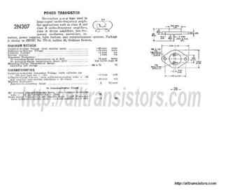
2N30 Specs and Replacement
Type Designator: 2N30
Material of Transistor: Ge
Polarity: PNP
Absolute Maximum Ratings
Maximum Collector Power Dissipation (Pc): 0.1 W
Maximum Collector-Base Voltage |Vcb|: 30 V
Maximum Collector-Emitter Voltage |Vce|: 30 V
Maximum Collector Current |Ic max|: 0.007 A
Max. Operating Junction Temperature (Tj): 100 °C
Electrical Characteristics
Transition Frequency (ft): 2 MHz
Collector Capacitance (Cc): 20 pF
Forward Current Transfer Ratio (hFE), MIN: 22
Package: TO7
2N30 Substitution
- BJT ⓘ Cross-Reference Search
2N30 datasheet
2n3055a mj2955a mj15015 mj15016.pdf ![]()
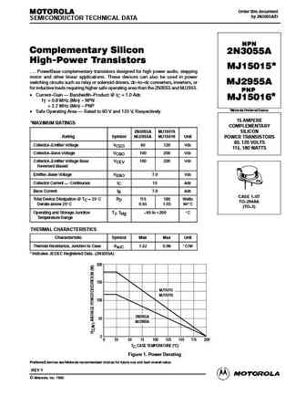
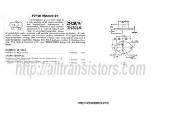
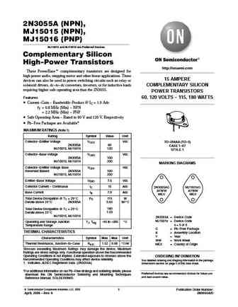
Order this document MOTOROLA by 2N3055A/D SEMICONDUCTOR TECHNICAL DATA NPN Complementary Silicon 2N3055A High-Power Transistors * MJ15015 . . . PowerBase complementary transistors designed for high power audio, stepping motor and other linear applications. These devices can also be used in power switching circuits such as relay or solenoid drivers, dc to dc converters, inverters... See More ⇒

Order this document MOTOROLA by 2N3055/D SEMICONDUCTOR TECHNICAL DATA NPN 2N3055 * Complementary Silicon Power PNP MJ2955* Transistors . . . designed for general purpose switching and amplifier applications. *Motorola Preferred Device DC Current Gain hFE = 20 70 @ IC = 4 Adc Collector Emitter Saturation Voltage 15 AMPERE VCE(sat) = 1.1 Vdc (Max) @ IC = 4 Adc P... See More ⇒
Order this document MOTOROLA by 2N3055/D SEMICONDUCTOR TECHNICAL DATA NPN 2N3055 * Complementary Silicon Power PNP MJ2955* Transistors . . . designed for general purpose switching and amplifier applications. *Motorola Preferred Device DC Current Gain hFE = 20 70 @ IC = 4 Adc Collector Emitter Saturation Voltage 15 AMPERE VCE(sat) = 1.1 Vdc (Max) @ IC = 4 Adc P... See More ⇒
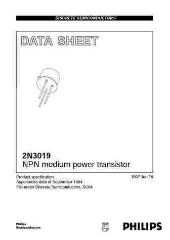
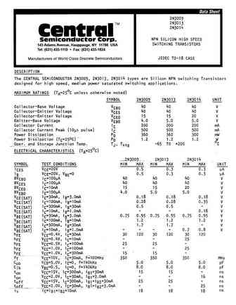
DISCRETE SEMICONDUCTORS DATA SHEET book, halfpage M3D111 2N3019 NPN medium power transistor 1997 Jun 19 Product specification Supersedes data of September 1994 File under Discrete Semiconductors, SC04 Philips Semiconductors Product specification NPN medium power transistor 2N3019 FEATURES PINNING High current (max. 1 A) PIN DESCRIPTION Low voltage (max. 80 V). 1 emitter... See More ⇒
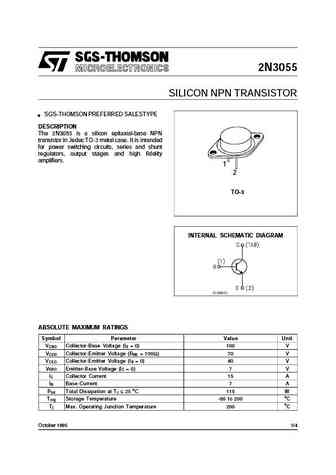
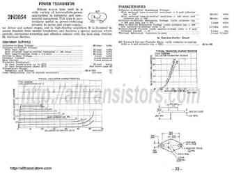
2N3055 SILICON NPN TRANSISTOR n SGS-THOMSON PREFERRED SALESTYPE DESCRIPTION The 2N3055 is a silicon epitaxial-base NPN transistor in Jedec TO-3 metal case. It is intended for power switching circuits, series and shunt regulators, output stages and high fidelity amplifiers. 1 2 TO-3 INTERNAL SCHEMATIC DIAGRAM ABSOLUTE MAXIMUM RATINGS Symbol Parameter Value Unit VCBO Collector-Base... See More ⇒
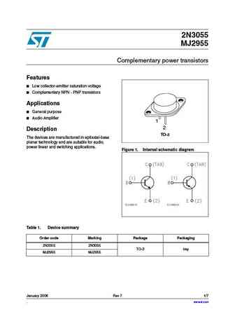
2N3055 MJ2955 Complementary power transistors Features Low collector-emitter saturation voltage Complementary NPN - PNP transistors Applications General purpose Audio Amplifier 1 2 Description TO-3 The devices are manufactured in epitaxial-base planar technology and are suitable for audio, power linear and switching applications. Figure 1. Internal schematic d... See More ⇒

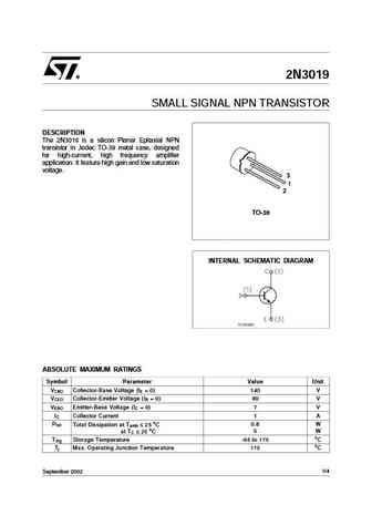
2N3019 SMALL SIGNAL NPN TRANSISTOR DESCRIPTION The 2N3019 is a silicon Planar Epitaxial NPN transistor in Jedec TO-39 metal case, designed for high-current, high frequency amplifier application. It feature high gain and low saturation voltage. TO-39 INTERNAL SCHEMATIC DIAGRAM ABSOLUTE MAXIMUM RATINGS Symbol Parameter Value Unit VCBO Collector-Base Voltage (IE = 0) 140 V VCEO C... See More ⇒
2N3019 SMALL SIGNAL NPN TRANSISTOR DESCRIPTION The 2N3019 is a silicon Planar Epitaxial NPN transistor in Jedec TO-39 metal case, designed for high-current, high frequency amplifier application. It feature high gain and low saturation voltage. TO-39 INTERNAL SCHEMATIC DIAGRAM ABSOLUTE MAXIMUM RATINGS Symbol Parameter Value Unit VCBO Collector-Base Voltage (IE = 0) 140 V VCEO C... See More ⇒
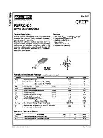
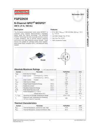
May 2000 TM QFET QFET QFET QFET 300V N-ChanneI MOSFET GeneraI Description Features These N-Channel enhancement mode power field effect 12A, 300V, RDS(on) = 0.16 @VGS = 10 V transistors are produced using Fairchild s proprietary, Low gate charge ( typical 47 nC) planar stripe, DMOS technology. Low Crss ( typical 40 pF) This advanced technology has been es... See More ⇒
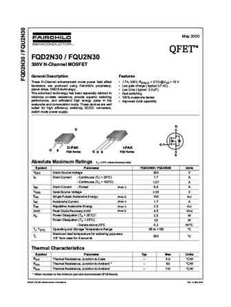
May 2000 TM QFET QFET QFET QFET FQD2N30 / FQU2N30 300V N-ChanneI MOSFET GeneraI Description Features These N-Channel enhancement mode power field effect 1.7A, 300V, RDS(on) = 3.7 @VGS = 10 V transistors are produced using Fairchild s proprietary, Low gate charge ( typical 3.7 nC) planar stripe, DMOS technology. Low Crss ( typical 3.0 pF) This advanced technology h... See More ⇒
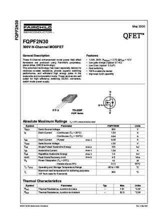
May 2000 TM QFET QFET QFET QFET 300V N-ChanneI MOSFET GeneraI Description Features These N-Channel enhancement mode power field effect 1.34A, 300V, RDS(on) = 3.7 @VGS = 10 V transistors are produced using Fairchild s proprietary, Low gate charge ( typical 3.7 nC) planar stripe, DMOS technology. Low Crss ( typical 3.0 pF) This advanced technology has been ... See More ⇒

May 2000 TM QFET QFET QFET QFET 300V N-ChanneI MOSFET GeneraI Description Features These N-Channel enhancement mode power field effect 21A, 300V, RDS(on) = 0.16 @VGS = 10 V transistors are produced using Fairchild s proprietary, Low gate charge ( typical 47 nC) planar stripe, DMOS technology. Low Crss ( typical 40 pF) This advanced technology has been esp... See More ⇒
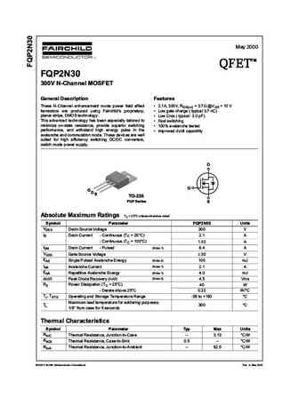
May 2000 TM QFET QFET QFET QFET 300V N-ChanneI MOSFET GeneraI Description Features These N-Channel enhancement mode power field effect 2.1A, 300V, RDS(on) = 3.7 @VGS = 10 V transistors are produced using Fairchild s proprietary, Low gate charge ( typical 3.7 nC) planar stripe, DMOS technology. Low Crss ( typical 3.0 pF) This advanced technology has been es... See More ⇒
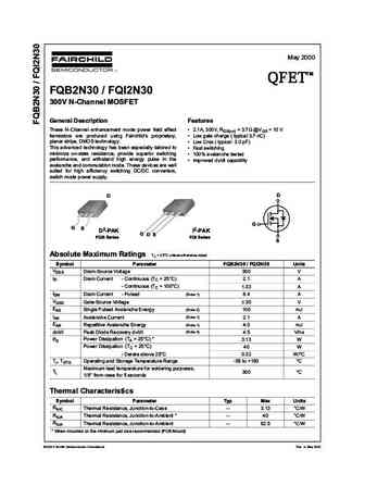
May 2000 TM QFET QFET QFET QFET FQB2N30 / FQI2N30 300V N-ChanneI MOSFET GeneraI Description Features These N-Channel enhancement mode power field effect 2.1A, 300V, RDS(on) = 3.7 @VGS = 10 V transistors are produced using Fairchild s proprietary, Low gate charge ( typical 3.7 nC) planar stripe, DMOS technology. Low Crss ( typical 3.0 pF) This advanced technology h... See More ⇒
145 Adams Avenue, Hauppauge, NY 11788 USA Tel (631) 435-1110 Fax (631) 435-1824 ... See More ⇒
145 Adams Avenue, Hauppauge, NY 11788 USA Tel (631) 435-1110 Fax (631) 435-1824 ... See More ⇒
145 Adams Avenue, Hauppauge, NY 11788 USA Tel (631) 435-1110 Fax (631) 435-1824 ... See More ⇒
145 Adams Avenue, Hauppauge, NY 11788 USA Tel (631) 435-1110 Fax (631) 435-1824 ... See More ⇒

VCES = 300V IXGA42N30C3 GenX3TM 300V IGBT IC110 = 42A IXGH42N30C3 VCE(sat) 1.85V High Speed PT IGBTs for IXGP42N30C3 50-150kHz switching tfi typ = 65ns TO-263 (IXGA) Symbol Test Conditions Maximum Ratings VCES TJ = 25 C to 150 C 300 V G VCGR TJ = 25 C to 150 C, RGE = 1M 300 V E C (TAB) VGES Continuous 20 V TO-247 (IXGH) VGEM Transient 30 V... See More ⇒

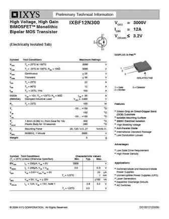
High Voltage, High Gain VCES = 3000V IXBT12N300 BIMOSFETTM Monolithic IXBH12N300 IC110 = 12A Bipolar MOS Transistor VCE(sat) 3.2V TO-268 (IXBT) G Symbol Test Conditions Maximum Ratings E VCES TC = 25 C to 150 C 3000 V C (Tab) VCGR TJ = 25 C to 150 C, RGE = 1M 3000 V VGES Continuous 20 V TO-247 (IXBH) VGEM Transient 30 V IC25 TC = 25 C 30 A ... See More ⇒
ixth2n300p3hv ixtt2n300p3hv.pdf ![]()
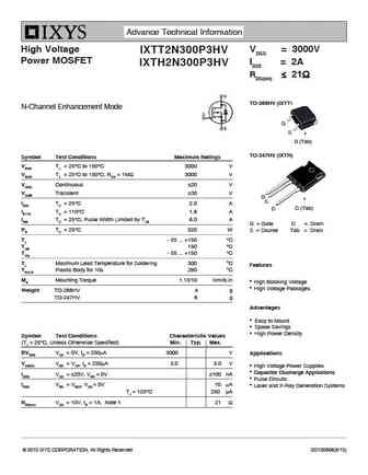
Advance Technical Information High Voltage VDSS = 3000V IXTT2N300P3HV Power MOSFET ID25 = 2A IXTH2N300P3HV RDS(on) 21 TO-268HV (IXTT) N-Channel Enhancement Mode G S D (Tab) TO-247HV (IXTH) Symbol Test Conditions Maximum Ratings VDSS TJ = 25 C to 150 C 3000 V VDGR TJ = 25 C to 150 C, RGS = 1M 3000 V VGSS Continuous 20 V V... See More ⇒
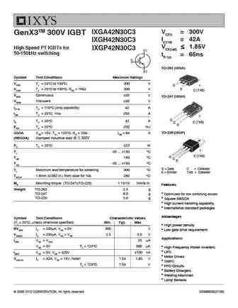
VCES = 300V IXGA42N30C3 GenX3TM 300V IGBT IC110 = 42A IXGH42N30C3 VCE(sat) 1.85V High Speed PT IGBTs for IXGP42N30C3 50-150kHz switching tfi typ = 65ns TO-263 (IXGA) Symbol Test Conditions Maximum Ratings VCES TJ = 25 C to 150 C 300 V G VCGR TJ = 25 C to 150 C, RGE = 1M 300 V E C (TAB) VGES Continuous 20 V TO-247 (IXGH) VGEM Transient 30 V... See More ⇒

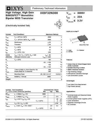
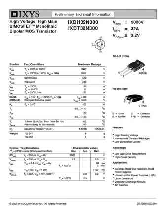
Preliminary Technical Information High Voltage, High Gain VCES = 3000V IXBH32N300 BIMOSFETTM Monolithic IXBT32N300 IC110 = 32A Bipolar MOS Transistor VCE(sat) 3.2V TO-247 (IXBH) Symbol Test Conditions Maximum Ratings VCES TC = 25 C to 150 C 3000 V G C (TAB) VCGR TJ = 25 C to 150 C, RGE = 1M 3000 V C E VGES Continuous 20 V VGEM Transient 30 V... See More ⇒
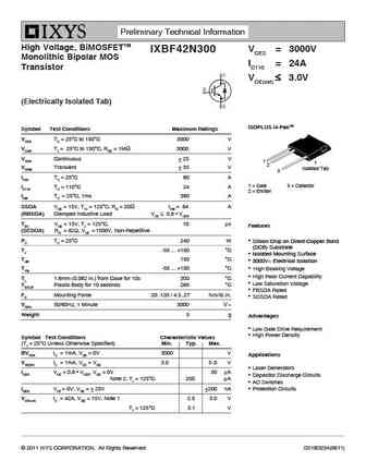
Preliminary Technical Information High Voltage, BiMOSFETTM VCES = 3000V IXBF42N300 Monolithic Bipolar MOS IC110 = 24A Transistor VCE(sat) 3.0V (Electrically Isolated Tab) ISOPLUS i4-PakTM Symbol Test Conditions Maximum Ratings VCES TC = 25 C to 150 C 3000 V VCGR TJ = 25 C to 150 C, RGE = 1M 3000 V VGES Continuous 25 V 1 2 VGEM Transient 35 V ... See More ⇒
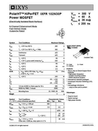
VDSS = 300 V IXFR 102N30P PolarHTTM HiPerFET ID25 = 60 A Power MOSFET RDS(on) 36 m (Electrically Isolated Back Surface) trr 200 ns N-Channel Enhancement Mode Fast Intrinsic Diode Avalanche Rated Symbol Test Conditions Maximum Ratings ISOPLUS247 (IXFR) VDSS TJ = 25 C to 150 C 300 V E153432 VDGR TJ = 25 C to 1... See More ⇒
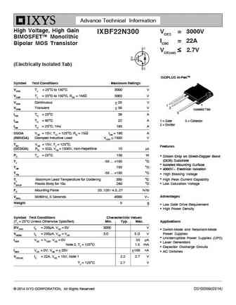
Advance Technical Information High Voltage, High Gain VCES = 3000V IXBF22N300 BIMOSFETTM Monolithic IC90 = 22A Bipolar MOS Transistor VCE(sat) 2.7V (Electrically Isolated Tab) ISOPLUS i4-PakTM Symbol Test Conditions Maximum Ratings VCES TJ = 25 C to 150 C 3000 V VCGR TJ = 25 C to 150 C, RGE = 1M 3000 V VGES Continuous 20 V 1 2 VGEM Transient ... See More ⇒
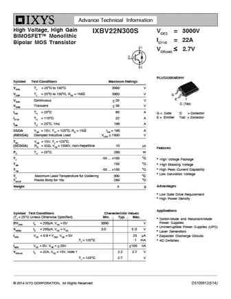
Advance Technical Information High Voltage, High Gain VCES = 3000V IXBV22N300S BIMOSFETTM Monolithic IC110 = 22A Bipolar MOS Transistor VCE(sat) 2.7V PLUS220SMDHV Symbol Test Conditions Maximum Ratings VCES TJ = 25 C to 150 C 3000 V VCGR TJ = 25 C to 150 C, RGE = 1M 3000 V G E VGES Continuous 20 V C (Tab) VGEM Transient 30 V IC25 TC = 25 C ... See More ⇒
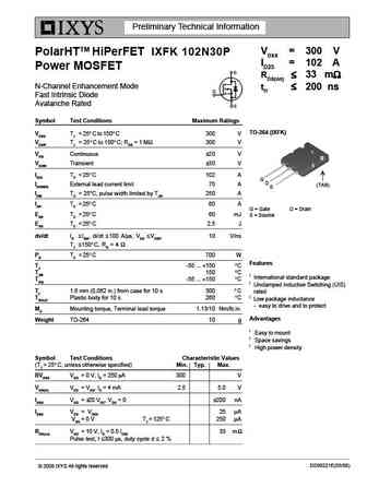
Preliminary Technical Information VDSS = 300 V IXFK 102N30P PolarHTTM HiPerFET ID25 = 102 A Power MOSFET RDS(on) 33 m N-Channel Enhancement Mode trr 200 ns Fast Intrinsic Diode Avalanche Rated Symbol Test Conditions Maximum Ratings TO-264 (IXFK) VDSS TJ = 25 C to 150 C 300 V VDGR TJ = 25 C to 150 C; RGS = ... See More ⇒
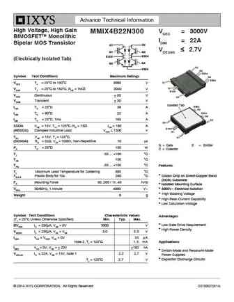
Advance Technical Information High Voltage, High Gain VCES = 3000V MMIX4B22N300 BIMOSFETTM Monolithic IC90 = 22A Bipolar MOS Transistor C2 C1 VCE(sat) 2.7V G1 G2 E2C4 E1C3 (Electrically Isolated Tab) G3 G4 C2 E3E4 G2 E2C4 Symbol Test Conditions Maximum Ratings G4 E3E4 C1 VCES TJ = 25 C to 150 C 3000 ... See More ⇒
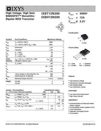
High Voltage, High Gain VCES = 3000V IXBT12N300 BIMOSFETTM Monolithic IXBH12N300 IC110 = 12A Bipolar MOS Transistor VCE(sat) 3.2V TO-268 (IXBT) G Symbol Test Conditions Maximum Ratings E VCES TC = 25 C to 150 C 3000 V C (Tab) VCGR TJ = 25 C to 150 C, RGE = 1M 3000 V VGES Continuous 20 V TO-247 (IXBH) VGEM Transient 30 V IC25 TC = 25 C 30 A ... See More ⇒
ixfh52n30q ixfk52n30q ixft52n30q.pdf ![]()
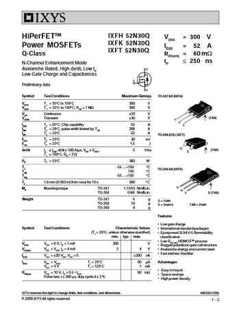
IXFH 52N30Q HiPerFETTM VDSS = 300 V IXFK 52N30Q Power MOSFETs ID25 = 52 A IXFT 52N30Q Q-Class RDS(on) = 60 mW trr 250 ns N-Channel Enhancement Mode Avalanche Rated, High dv/dt, Low trr Low Gate Charge and Capacitances Preliminary data Symbol Test Conditions Maximum Ratings TO-247 AD (IXFH) VDSS TJ = 25 C to 150 C 300 V VDGR TJ = 25 C to 150 C; RGS = 1 MW 300 V VGS Continuo... See More ⇒
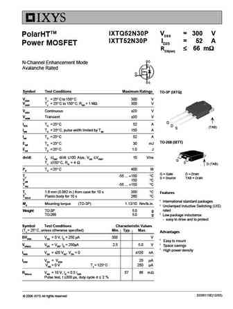
IXTQ52N30P VDSS = 300 V PolarHTTM IXTT52N30P ID25 = 52 A Power MOSFET RDS(on) 66 m N-Channel Enhancement Mode Avalanche Rated Symbol Test Conditions Maximum Ratings TO-3P (IXTQ) VDSS TJ = 25 C to 150 C 300 V VDGR TJ = 25 C to 150 C; RGS = 1 M 300 V VGSS Continuous 20 V VGSM Transient 30 V G ID25 TC = 25 C52 A D (TAB) ... See More ⇒
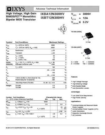
Advance Technical Information High Voltage, High Gain VCES = 3000V IXBA12N300HV BIMOSFETTM Monolithic IXBT12N300HV IC110 = 12A Bipolar MOS Transistor VCE(sat) 3.2V TO-263 (IXBA) G E C (Tab) Symbol Test Conditions Maximum Ratings VCES TC = 25 C to 150 C 3000 V TO-268 (IXBT) VCGR TJ = 25 C to 150 C, RGE = 1M 3000 V VGES Continuous 20 V VGEM Trans... See More ⇒

Preliminary Technical Information High Voltage, BiMOSFETTM VCES = 3000V IXBT42N300HV Monolithic Bipolar MOS IXBH42N300HV IC110 = 42A Transistor VCE(sat) 3.0V TO-268HV (IXBT) G E Symbol Test Conditions Maximum Ratings C (Tab) VCES TC = 25 C to 150 C 3000 V VCGR TJ = 25 C to 150 C, RGE = 1M 3000 V TO-247HV (IXBH) VGES Continuous 25 V VGEM Trans... See More ⇒
Preliminary Technical Information High Voltage, High Gain VCES = 3000V IXBF32N300 BIMOSFETTM Monolithic IC90 = 22A Bipolar MOS Transistor VCE(sat) 3.2V (Electrically Isolated Tab) ISOPLUS i4-PakTM Symbol Test Conditions Maximum Ratings VCES TC = 25 C to 150 C 3000 V 1 VCGR TJ = 25 C to 150 C, RGE = 1M 3000 V 2 VGES Continuous 20 V 5 VGEM Transie... See More ⇒
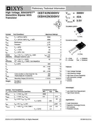
Preliminary Technical Information High Voltage, BiMOSFETTM VCES = 3000V IXBT42N300HV Monolithic Bipolar MOS IXBH42N300HV IC110 = 42A Transistor VCE(sat) 3.0V TO-268HV (IXBT) G E Symbol Test Conditions Maximum Ratings C (Tab) VCES TC = 25 C to 150 C 3000 V VCGR TJ = 25 C to 150 C, RGE = 1M 3000 V TO-247HV (IXBH) VGES Continuous 25 V VGEM Trans... See More ⇒

Advance Technical Information High Voltage, High Gain VCES = 3000V IXBT22N300HV BIMOSFETTM Monolithic IXBH22N300HV IC110 = 22A Bipolar MOS Transistor VCE(sat) 2.7V TO-268HV (IXBT) Symbol Test Conditions Maximum Ratings G VCES TJ = 25 C to 150 C 3000 V E C (Tab) VCGR TJ = 25 C to 150 C, RGE = 1M 3000 V VGES Continuous 20 V TO-247HV (IXBH) VGEM ... See More ⇒
Preliminary Technical Information High Voltage, High Gain VCES = 3000V IXBF12N300 BIMOSFETTM Monolithic IC90 = 12A Bipolar MOS Transistor VCE(sat) 3.2V (Electrically Isolated Tab) ISOPLUS i4-PakTM Symbol Test Conditions Maximum Ratings VCES TC = 25 C to 150 C 3000 V 1 VCGR TJ = 25 C to 150 C, RGE = 1M 3000 V 2 VGES Continuous 20 V 5 VGEM Transie... See More ⇒

VCES = 300V IXGA42N30C3 GenX3TM 300V IGBT IC110 = 42A IXGH42N30C3 VCE(sat) 1.85V High Speed PT IGBTs for IXGP42N30C3 50-150kHz switching tfi typ = 65ns TO-263 (IXGA) Symbol Test Conditions Maximum Ratings VCES TJ = 25 C to 150 C 300 V G VCGR TJ = 25 C to 150 C, RGE = 1M 300 V E C (TAB) VGES Continuous 20 V TO-247 (IXGH) VGEM Transient 30 V... See More ⇒

Advance Technical Information High Voltage, High Gain VCES = 3000V IXBA12N300HV BIMOSFETTM Monolithic IXBT12N300HV IC110 = 12A Bipolar MOS Transistor VCE(sat) 3.2V TO-263 (IXBA) G E C (Tab) Symbol Test Conditions Maximum Ratings VCES TC = 25 C to 150 C 3000 V TO-268 (IXBT) VCGR TJ = 25 C to 150 C, RGE = 1M 3000 V VGES Continuous 20 V VGEM Trans... See More ⇒
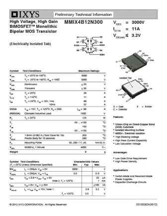
Preliminary Technical Information High Voltage, High Gain MMIX4B12N300 VCES = 3000V BIMOSFETTM Monolithic IC110 = 11A Bipolar MOS Transistor VCE(sat) 3.2V C2 C1 G1 G2 (Electrically Isolated Tab) E2C4 E1C3 G3 G4 C2 G2 E3E4 E2C4 G4 E3E4 C1 G1 E1C3 Symbol Test Conditions Maximum Ratings G3 VCES TC = 25 C to 150 C 3000 V Isolated Tab E3E4 VCG... See More ⇒
Preliminary Technical Information High Voltage, High Gain VCES = 3000V IXBH32N300 BIMOSFETTM Monolithic IXBT32N300 IC110 = 32A Bipolar MOS Transistor VCE(sat) 3.2V TO-247 (IXBH) Symbol Test Conditions Maximum Ratings VCES TC = 25 C to 150 C 3000 V G C (TAB) VCGR TJ = 25 C to 150 C, RGE = 1M 3000 V C E VGES Continuous 20 V VGEM Transient 30 V... See More ⇒
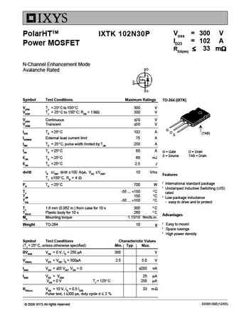
VDSS = 300 V IXTK 102N30P PolarHTTM ID25 = 102 A Power MOSFET RDS(on) 33 m N-Channel Enhancement Mode Avalanche Rated Symbol Test Conditions Maximum Ratings TO-264 (IXTK) VDSS TJ = 25 C to 150 C 300 V VDGR TJ = 25 C to 150 C; RGS = 1 M 300 V VGSS Continuous 20 V VGSM Transient 30 V G ID25 TC = 25 C 102 A D (TAB) S ID(... See More ⇒
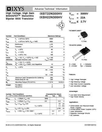
Advance Technical Information High Voltage, High Gain VCES = 3000V IXBT22N300HV BIMOSFETTM Monolithic IXBH22N300HV IC110 = 22A Bipolar MOS Transistor VCE(sat) 2.7V TO-268HV (IXBT) Symbol Test Conditions Maximum Ratings G VCES TJ = 25 C to 150 C 3000 V E C (Tab) VCGR TJ = 25 C to 150 C, RGE = 1M 3000 V VGES Continuous 20 V TO-247HV (IXBH) VGEM ... See More ⇒

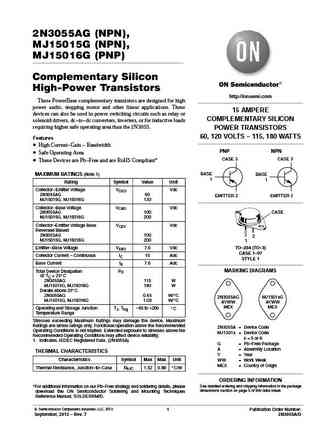
2N3055A (NPN), MJ15015 (NPN), MJ15016 (PNP) MJ15015 and MJ15016 are Preferred Devices Complementary Silicon High-Power Transistors http //onsemi.com These PowerBaset complementary transistors are designed for high power audio, stepping motor and other linear applications. These 15 AMPERE devices can also be used in power switching circuits such as relay or solenoid drivers, dc-to-dc ... See More ⇒

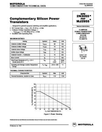
2N3055(NPN), MJ2955(PNP) Preferred Device Complementary Silicon Power Transistors Complementary silicon power transistors are designed for general-purpose switching and amplifier applications. Features http //onsemi.com DC Current Gain - hFE = 20-70 @ IC = 4 Adc Collector-Emitter Saturation Voltage - 15 AMPERE VCE(sat) = 1.1 Vdc (Max) @ IC = 4 Adc POWER TRANSISTORS Exc... See More ⇒
2N3055A (NPN), MJ15015 (NPN), MJ15016 (PNP) MJ15015 and MJ15016 are Preferred Devices Complementary Silicon High-Power Transistors http //onsemi.com These PowerBaset complementary transistors are designed for high power audio, stepping motor and other linear applications. These 15 AMPERE devices can also be used in power switching circuits such as relay or solenoid drivers, dc-to-dc ... See More ⇒
2n3055ag mj15015g mj15016g.pdf ![]()
2N3055AG (NPN), MJ15015G (NPN), MJ15016G (PNP) Complementary Silicon High-Power Transistors http //onsemi.com These PowerBase complementary transistors are designed for high power audio, stepping motor and other linear applications. These 15 AMPERE devices can also be used in power switching circuits such as relay or COMPLEMENTARY SILICON solenoid drivers, dc-to-dc converters, invert... See More ⇒
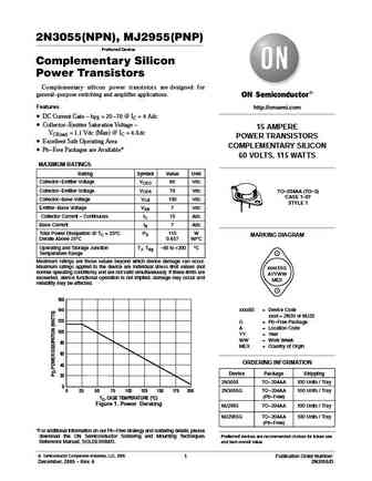
2N3055(NPN), MJ2955(PNP) Preferred Device Complementary Silicon Power Transistors Complementary silicon power transistors are designed for general-purpose switching and amplifier applications. Features http //onsemi.com DC Current Gain - hFE = 20-70 @ IC = 4 Adc Collector-Emitter Saturation Voltage - 15 AMPERE VCE(sat) = 1.1 Vdc (Max) @ IC = 4 Adc POWER TRANSISTORS Exc... See More ⇒
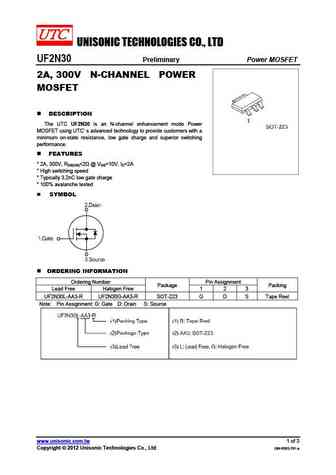
UNISONIC TECHNOLOGIES CO., LTD UF2N30 Preliminary Power MOSFET 2A, 300V N-CHANNEL POWER MOSFET DESCRIPTION The UTC UF2N30 is an N-channel enhancement mode Power MOSFET using UTC s advanced technology to provide customers with a minimum on-state resistance, low gate charge and superior switching performance. FEATURES * 2A, 300V, RDS(ON)... See More ⇒
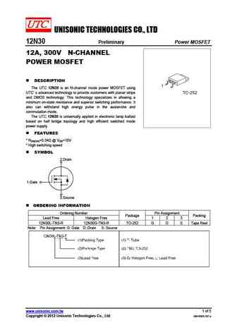
UNISONIC TECHNOLOGIES CO., LTD 12N30 Preliminary Power MOSFET 12A, 300V N-CHANNEL POWER MOSFET DESCRIPTION The UTC 12N30 is an N-channel mode power MOSFET using UTC s advanced technology to provide customers with planar stripe and DMOS technology. This technology specializes in allowing a minimum on-state resistance and superior switching performance. It also can withstand ... See More ⇒
UTC 2N3055 SILICON NPN TRANSISTOR SILICON NPN TRANSISTORS The UTC 2N3055 is a silicon NPN transistor in TO-3 metal case. It is intended for power switching circuits, series and shunt regulators, output stages and high fidelity amplifiers. TO-3 ABSOLUTE MAXIMUM RATINGS ( Ta=25 C ,unless otherwise specified ) PARAMETERS SYMBOL VALUE UNITS Collector-Base Voltage VCBO 100 V Collector-Em... See More ⇒
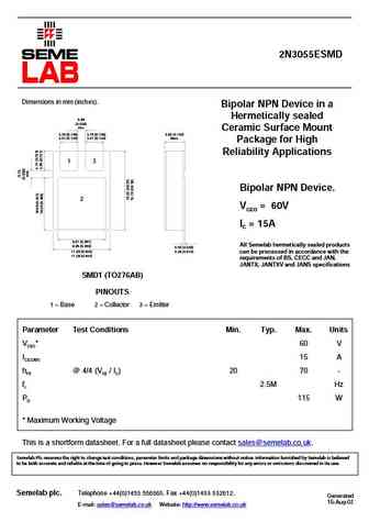
2N3055ESMD Dimensions in mm (inches). Bipolar NPN Device in a Hermetically sealed 0.89 (0.035) min. Ceramic Surface Mount 3.70 (0.146) 3.70 (0.146) 3.60 (0.142) 3.41 (0.134) 3.41 (0.134) Max. Package for High Reliability Applications 1 3 Bipolar NPN Device. 2 VCEO = 60V IC = 15A 9.67 (0.381) All Semelab hermetically sealed products 9.38 (0.369) 0.50 (0.020) 0.26 ... See More ⇒

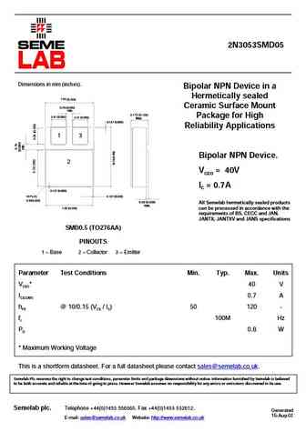
2N3053SMD Dimensions in mm (inches). Bipolar NPN Device in a Hermetically sealed 0.89 (0.035) min. Ceramic Surface Mount 3.70 (0.146) 3.70 (0.146) 3.60 (0.142) 3.41 (0.134) 3.41 (0.134) Max. Package for High Reliability Applications 1 3 Bipolar NPN Device. 2 VCEO = 40V IC = 0.7A 9.67 (0.381) All Semelab hermetically sealed products 9.38 (0.369) 0.50 (0.020) 0.26 ... See More ⇒
2N3053SMD05 Dimensions in mm (inches). Bipolar NPN Device in a Hermetically sealed 7.54 (0.296) 0.76 (0.030) Ceramic Surface Mount min. 3.175 (0.125) 2.41 (0.095) Package for High 2.41 (0.095) Max. 0.127 (0.005) Reliability Applications 1 3 Bipolar NPN Device. 2 VCEO = 40V IC = 0.7A 0.127 (0.005) 16 PLCS 0.127 (0.005) 0.50(0.020) 0.50 (0.020) All Semelab he... See More ⇒
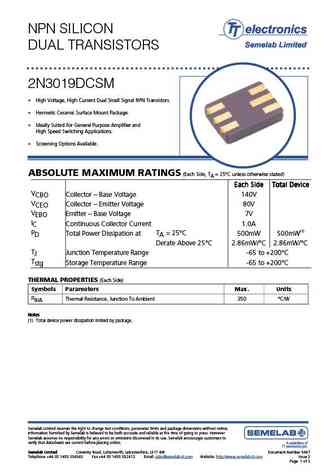
NPN SILICON DUAL TRANSISTORS 2N3019DCSM High Voltage, High Current Dual Small Signal NPN Transistors. Hermetic Ceramic Surface Mount Package. Ideally Suited For General Purpose Amplifier and High Speed Switching Applications. Screening Options Available. ABSOLUTE MAXIMUM RATINGS (Each Side, TA = 25 C unless otherwise stated) Each Side Total Device Each Side... See More ⇒
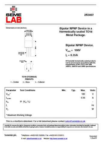
2N3007 Dimensions in mm (inches). Bipolar NPNP Device in a 5.84 (0.230) 5.31 (0.209) Hermetically sealed TO18 4.95 (0.195) 4.52 (0.178) Metal Package. Bipolar NPNP Device. VCEO = 100V 0.48 (0.019) 0.41 (0.016) dia. IC = 0.35A 2.54 (0.100) All Semelab hermetically sealed products Nom. can be processed in accordance with the requirements of BS, CECC and JAN, JANTX,... See More ⇒
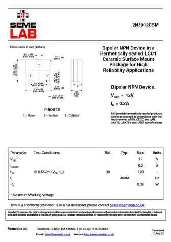
2N3012CSM Dimensions in mm (inches). Bipolar NPN Device in a 0.51 0.10 Hermetically sealed LCC1 (0.02 0.004) 0.31 rad. (0.012) Ceramic Surface Mount 3 Package for High Reliability Applications 21 1.91 0.10 (0.075 0.004) A 0.31 rad. Bipolar NPN Device. (0.012) 3.05 0.13 (0.12 0.005) 1.40 (0.055) 1.02 0.10 max. VCEO = 12V A = (0.04 0.004... See More ⇒
Boca Semiconductor Corp. BSC http //www.bocasemi.com ... See More ⇒
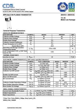
Continental Device India Limited An ISO/TS 16949, ISO 9001 and ISO 14001 Certified Company NPN SILICON PLANAR TRANSISTOR 2N3053 / 2N3053A TO-39 Metal Can Package General Purpose Transistors ABSOLUTE MAXIMUM RATINGS DESCRIPTION SYMBOL 2N3053 2N3053A UNIT Collector Emitter Voltage VCEO 40 60 V Collector Base Voltage VCBO 60 80 V Emitter Base Voltage VEBO 5.0 V Collector Current Continu... See More ⇒
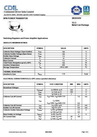
Continental Device India Limited An ISO/TS 16949, ISO 9001 and ISO 14001 Certified Company 2N3055HV NPN POWER TRANSISTOR TO-3 Metal Can Package Switching Regulator and Power Amplifier Applications ABSOLUTE MAXIMUM RATINGS DESCRIPTION SYMBOL VALUE UNITS VCBO Collector Base Voltage ( Open Emitter) V 100 VCEO Collector Emitter Voltage (Open Base) V 100 VEBO Emitter Base Voltage V ... See More ⇒
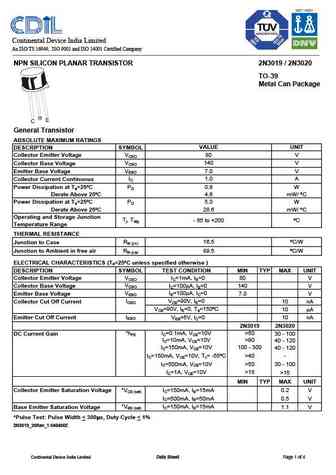
Continental Device India Limited An ISO/TS 16949, ISO 9001 and ISO 14001 Certified Company NPN SILICON PLANAR TRANSISTOR 2N3019 / 2N3020 TO-39 Metal Can Package General Transistor ABSOLUTE MAXIMUM RATINGS DESCRIPTION SYMBOL VALUE UNIT Collector Emitter Voltage VCEO 80 V Collector Base Voltage VCBO 140 V Emitter Base Voltage VEBO 7.0 V Collector Current Continuous IC 1.0 A Power Diss... See More ⇒
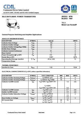
Continental Device India Limited An ISO/TS 16949, ISO 9001 and ISO 14001 Certified Company 2N3055 NPN SILICON PLANAR POWER TRANSISTORS MJ2955 PNP TO-3 Metal Can Package General Purpose Switching and Amplifier Applications ABSOLUTE MAXIMUM RATINGS DESCRIPTION SYMBOL UNITS VALUE Collector Base Voltage VCBO V 100 Collector Emitter Voltage VCEO V 60 Collector Emitter Voltage(RBE=100... See More ⇒
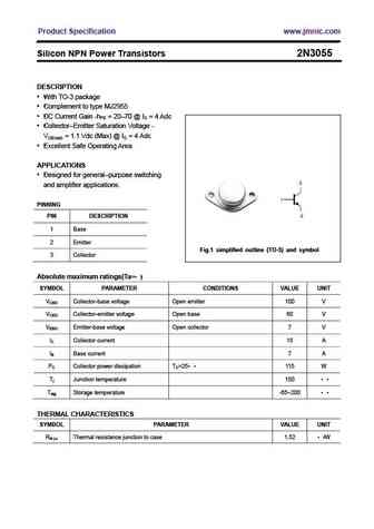
Product Specification www.jmnic.com Silicon NPN Power Transistors 2N3055 DESCRIPTION With TO-3 package Complement to type MJ2955 DC Current Gain -hFE = 20 70 @ IC = 4 Adc Collector Emitter Saturation Voltage - VCE(sat) = 1.1 Vdc (Max) @ IC = 4 Adc Excellent Safe Operating Area APPLICATIONS Designed for general purpose switching and amplifier applications. ... See More ⇒
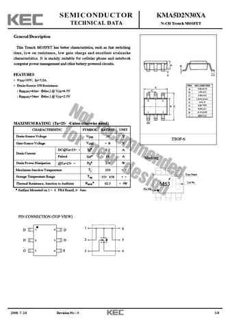
SEMICONDUCTOR KMA5D2N30XA TECHNICAL DATA N-CH Trench MOSFET General Description This Trench MOSFET has better characteristics, such as fast switching time, low on resistance, low gate charge and excellent avalanche characteristics. It is mainly suitable for cellular phone and netebook computer power management and other battery powered circuits. FEATURES VDSS=30V, ID=5.2A. Drain-S... See More ⇒
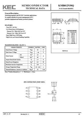
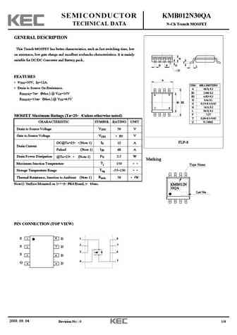
SEMICONDUCTOR KMB012N30Q TECHNICAL DATA N-Ch Trench MOSFET General Description Switching regulator and DC-DC Converter applications. It s mainly suitable for power management in PC, portable equipment and battery powered systems. H T D P G L FEATURES VDSS=30V, ID=12A. A Low Drain-Source ON Resistance. DIM MILLIMETERS RDS(ON)=7m (Max.) @ VGS=10V A 5.05+0.25/-0.20 RDS(ON)=11... See More ⇒
SEMICONDUCTOR KMB012N30QA TECHNICAL DATA N-Ch Trench MOSFET GENERAL DESCRIPTION This Trench MOSFET has better characteristics, such as fast switching time, low on resistance, low gate charge and excellent avalanche characteristiscs. It is mainly H suitable for DC/DC Converter and Battery pack.. T D P G L U FEATURES A VDSS=30V, ID=12A. DIM MILLIMETERS Drain to Source On Resis... See More ⇒
TECHNICAL DATA LOW POWER NPN SILICON TRANSISTOR Qualified per MIL-PRF-19500/391 Devices Qualified Level 2N3019 2N3057A 2N3700 JAN 2N3019S 2N3700S JANTX JANTXV JANS MAXIMUM RATINGS Ratings Symbol Value Units Collector-Emitter Voltage 80 Vdc VCEO Collector-Base Voltage 140 Vdc VCBO TO-39* (TO-205AD) Emitter-Base Voltage 7.0 Vdc VEBO 2N3019, 2N3019S Collector ... See More ⇒
AOT12N30/AOTF12N30 300V,11.5A N-Channel MOSFET General Description Product Summary VDS 350V@150 The AOT12N30/AOTF12N30 is fabricated using an advanced high voltage MOSFET process that is designed ID (at VGS=10V) 11.5A to deliver high levels of performance and robustness in RDS(ON) (at VGS=10V) ... See More ⇒

AOT12N30/AOTF12N30 300V,11.5A N-Channel MOSFET General Description Product Summary VDS 350V@150 The AOT12N30/AOTF12N30 is fabricated using an advanced high voltage MOSFET process that is designed ID (at VGS=10V) 11.5A to deliver high levels of performance and robustness in RDS(ON) (at VGS=10V) ... See More ⇒
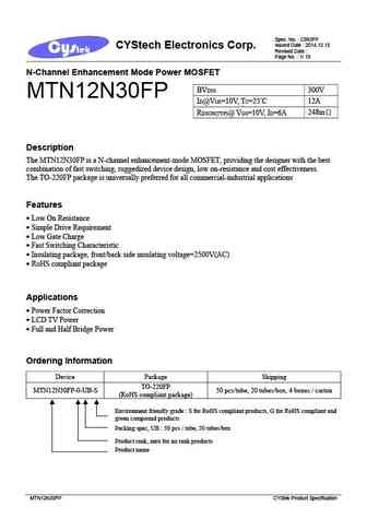
Spec. No. C993FP Issued Date 2014.12.15 CYStech Electronics Corp. Revised Date Page No. 1/ 10 N-Channel Enhancement Mode Power MOSFET BVDSS 300V MTN12N30FP ID@VGS=10V, TC=25 C 12A RDSON(TYP)@ VGS=10V, ID=6A 248m Description The MTN12N30FP is a N-channel enhancement-mode MOSFET, providing the designer with the best combination of fast switching, ruggedized devic... See More ⇒
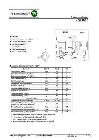
SMD Type SMD Type SMD Type SMD Type SMD Type IC SMD Type IC SMD Type IC SMD Type IC SMD Type Transistors SMD Type Transistors SMD Type Transistors SMD Type Transistors SMD Type SMD Type SMD Type SMD Type SMD Type SMD Type SMD Type SMD Type Product specification KQB2N30 TO-263 Unit mm Features 4.57+0.2 -0.2 +0.1 1.27-0.1 2.1A, 300 V. RDS(ON) =3.7 @VGS =10V Low gate... See More ⇒
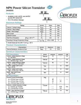
NPN Power Silicon Transistor 2N3055 Features Available in JAN, JANTX, and JANTXV per MIL-PRF-19500/407 TO-3 (TO-204AA) Package Maximum Ratings Ratings Symbol Value Units Collector - Emitter Voltage VCEO 70 Vdc Collector - Base Voltage VCBO 100 Vdc Emitter - Base Voltage VEBO 7.0 Vdc Base Current IB 7.0 Adc Collector Current IC 15 Adc Total Power Dissipation @ TA = 25 C (... See More ⇒
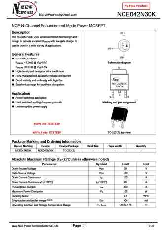
Pb Free Product http //www.ncepower.com NCE042N30K NCE N-Channel Enhancement Mode Power MOSFET Description The NCE042N30K uses advanced trench technology and design to provide excellent R with low gate charge. It DS(ON) can be used in a wide variety of applications. General Features V =30V,I =100A DS D R =3.2m @ V =10V Schematic diagram DS(ON) GS R =6.8m @ V =4.5V DS(ON) ... See More ⇒
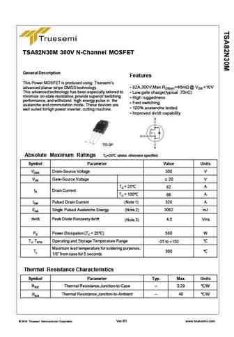
TSA82N30M 300V N-Channel MOSFET General Description Features This Power MOSFET is produced using Truesemi s 82A,300V,Max.RDS(on)=46m @ VGS =10V advanced planar stripe DMOS technology. This advanced technology has been especially tailored to Low gate charge(typical 70nC) minimize on-state resistance, provide superior switching High ruggedness performance, and withstand h... See More ⇒
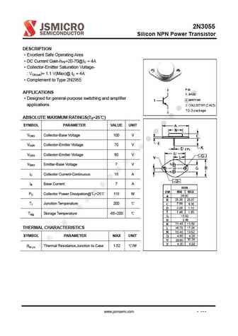
2N3055 Silicon NPN Power Transistor DESCRIPTION Excellent Safe Operating Area DC Current Gain-hFE=20-70@IC = 4A Collector-Emitter Saturation Voltage- VCE(sat)= 1.1 V(Max)@ IC = 4A Complement to Type 2N2955 APPLICATIONS Designed for general-purpose switching and amplifier applications ABSOLUTE MAXIMUM RATINGS(Ta=25 ) SYMBOL PARAMETER VALUE UNIT VCBO Collecto... See More ⇒
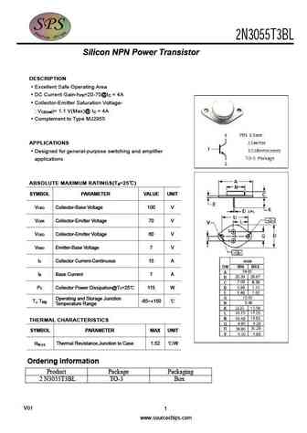
2N3055T3BL Silicon NPN Power Transistor DESCRIPTION Excellent Safe Operating Area DC Current Gain-h =20-70@I = 4A FE C Collector-Emitter Saturation Voltage- V )= 1.1 V(Max)@ I = 4A CE(sat C Complement to Type MJ2955 APPLICATIONS Designed for general-purpose switching and amplifier applications ABSOLUTE MAXIMUM RATINGS(T =25 ) a SYMBOL PARAMETER VALUE UNIT V Collect... See More ⇒
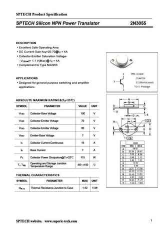
SPTECH Product Specification SPTECH Silicon NPN Power Transistor 2N3055 DESCRIPTION Excellent Safe Operating Area DC Current Gain-h =20-70@I = 4A FE C Collector-Emitter Saturation Voltage- V )= 1.1 V(Max)@ I = 4A CE(sat C Complement to Type MJ2955 APPLICATIONS Designed for general-purpose switching and amplifier applications ABSOLUTE MAXIMUM RATINGS(T =25 ) a SYMBOL... See More ⇒
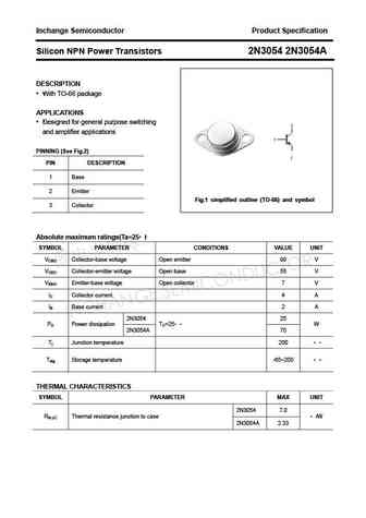
Inchange Semiconductor Product Specification Silicon NPN Power Transistors 2N3054 2N3054A DESCRIPTION With TO-66 package APPLICATIONS Designed for general purpose switching and amplifier applications PINNING (See Fig.2) PIN DESCRIPTION 1 Base 2 Emitter Fig.1 simplified outline (TO-66) and symbol 3 Collector Absolute maximum ratings(Ta=25 ) SYMBOL PARAMETER CONDITI... See More ⇒
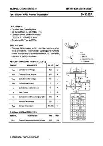
INCHANGE Semiconductor isc Product Specification isc Silicon NPN Power Transistor 2N3055A DESCRIPTION Excellent Safe Operating Area DC Current Gain-hFE=20-70@IC = 4A Collector-Emitter Saturation Voltage- VCE(sat)= 1.1 V(Max)@ IC = 4A Complement to Type MJ2955A APPLICATIONS Designed for high power audio, stepping motor and other linear applications. It can also be... See More ⇒
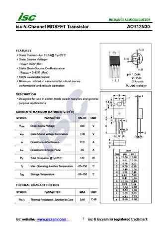
isc N-Channel MOSFET Transistor AOT12N30 FEATURES Drain Current I = 11.5A@ T =25 D C Drain Source Voltage- V = 300V(Min) DSS Static Drain-Source On-Resistance R = 0.42 (Max) DS(on) 100% avalanche tested Minimum Lot-to-Lot variations for robust device performance and reliable operation DESCRIPTION Designed for use in switch mode power supplies and general pu... See More ⇒

isc Silicon NPN Power Transistor 2N3055 DESCRIPTION Excellent Safe Operating Area DC Current Gain-h =20-70@I = 4A FE C Collector-Emitter Saturation Voltage- V )= 1.1 V(Max)@ I = 4A CE(sat C Complement to Type MJ2955 Minimum Lot-to-Lot variations for robust device performance and reliable operation APPLICATIONS Designed for general-purpose switching and amplifier appli... See More ⇒
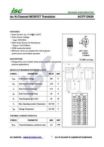
isc N-Channel MOSFET Transistor AOTF12N30 FEATURES Drain Current I = 11.5A@ T =25 D C Drain Source Voltage- V = 300V(Min) DSS Static Drain-Source On-Resistance R = 0.42 (Max) DS(on) 100% avalanche tested Minimum Lot-to-Lot variations for robust device performance and reliable operation DESCRIPTION Designed for use in switch mode power supplies and general p... See More ⇒
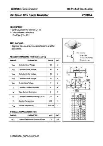
INCHANGE Semiconductor isc Product Specification isc Silicon NPN Power Transistor 2N3054 DESCRIPTION Continuous Collector Current-IC= 4A Collector Power Dissipation- PC= 25W @TC= 25 APPLICATIONS Designed for general purpose switching and amplifier applications. ABSOLUTE MAXIMUM RATINGS(Ta=25 ) SYMBOL PARAMETER VALUE UNIT VCBO Collector-Base Voltage 90 V V C... See More ⇒
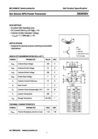
INCHANGE Semiconductor isc Product Specification isc Silicon NPN Power Transistor 2N3055H DESCRIPTION Excellent Safe Operating Area DC Current Gain-hFE=20-70@IC = 4A Collector-Emitter Saturation Voltage- VCE(sat)= 1.1 V(Max)@ IC = 4A APPLICATIONS Designed for general-purpose switching and amplifier Applications. ABSOLUTE MAXIMUM RATINGS(Ta=25 ) SYMBOL PARAMETER... See More ⇒
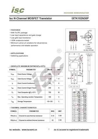
Isc N-Channel MOSFET Transistor IXTK102N30P FEATURES With To-3PL package Low input capacitance and gate charge Low gate input resistance 100% avalanche tested Minimum Lot-to-Lot variations for robust device performance and reliable operation APPLICATIONS Switching applications ABSOLUTE MAXIMUM RATINGS(T =25 ) a SYMBOL PARAMETER VALUE UNIT V Drain-Source Voltage ... See More ⇒
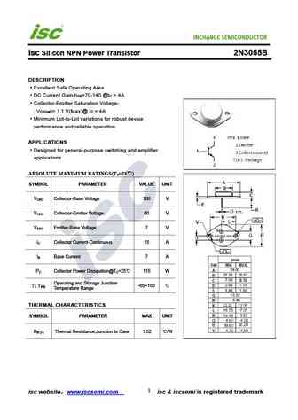
isc Silicon NPN Power Transistor 2N3055B DESCRIPTION Excellent Safe Operating Area DC Current Gain-h =70-140 @I = 4A FE C Collector-Emitter Saturation Voltage- V )= 1.1 V(Max)@ I = 4A CE(sat C Minimum Lot-to-Lot variations for robust device performance and reliable operation APPLICATIONS Designed for general-purpose switching and amplifier applications ABSOLUTE MAXIMUM ... See More ⇒
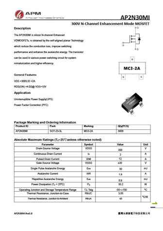
AP2N30MI 300V N-Channel Enhancement Mode MOSFET Description The AP2N30MI is silicon N-channel Enhanced VDMOSFETs, is obtained by the self-aligned planar Technology which reduce the conduction loss, improve switching performance and enhance the avalanche energy. The transistor can be used in various power switching circuit for system miniaturization and higher efficiency. Gen... See More ⇒
Detailed specifications: 2N2992 , 2N2993 , 2N2994 , 2N2995 , 2N2996 , 2N2997 , 2N2998 , 2N2999 , C5198 , 2N300 , 2N3000 , 2N3009 , 2N301 , 2N3010 , 2N3011 , 2N3012 , 2N3013 .
Keywords - 2N30 pdf specs
2N30 cross reference
2N30 equivalent finder
2N30 pdf lookup
2N30 substitution
2N30 replacement


LIST
Last Update
BJT: GA1A4M | SBT42 | 2SA200-Y
Popular searches
ru7088r mosfet | mp40 transistor | fgpf4636 datasheet | 2sc1945 | c2383 | 2sb681 | bc639 equivalent | bd138 transistor equivalent