BSS12 Specs and Replacement
Type Designator: BSS12
Material of Transistor: Si
Polarity: NPN
Absolute Maximum Ratings
Maximum Collector Power Dissipation (Pc): 0.36 W
Maximum Collector-Base Voltage |Vcb|: 30 V
Maximum Collector-Emitter Voltage |Vce|: 12 V
Maximum Emitter-Base Voltage |Veb|: 5 V
Maximum Collector Current |Ic max|: 0.2 A
Max. Operating Junction Temperature (Tj): 175 °C
Electrical Characteristics
Transition Frequency (ft): 400 MHz
Collector Capacitance (Cc): 3 pF
Forward Current Transfer Ratio (hFE), MIN: 30
Package: TO18
BSS12 Substitution
- BJT ⓘ Cross-Reference Search
BSS12 datasheet
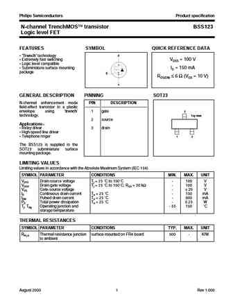
Philips Semiconductors Product specification N-channel TrenchMOS transistor BSS123 Logic level FET FEATURES SYMBOL QUICK REFERENCE DATA Trench technology d Extremely fast switching VDSS = 100 V Logic level compatible Subminiature surface mounting ID = 150 mA package g RDS(ON) 6 (VGS = 10 V) s GENERAL DESCRIPTION PINNING SOT23 N-channel enhancemen... See More ⇒
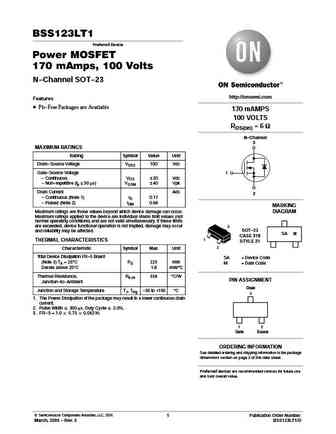
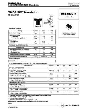
BSS123LT1 Preferred Device Power MOSFET 170 mAmps, 100 Volts N-Channel SOT-23 http //onsemi.com Features Pb-Free Packages are Available 170 mAMPS 100 VOLTS RDS(on) = 6 W N-Channel 3 MAXIMUM RATINGS Rating Symbol Value Unit Drain-Source Voltage VDSS 100 Vdc Gate-Source Voltage 1 - Continuous VGS 20 Vdc - Non-repetitive (tp 50 ms) VGSM 40 Vpk Drain Current Adc 2 -... See More ⇒
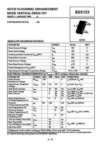
DISCRETE SEMICONDUCTORS DATA SHEET BSS123 N-channel enhancement mode vertical D-MOS transistor April 1995 Product specification File under Discrete Semiconductors, SC13b Philips Semiconductors Product specification N-channel enhancement mode vertical BSS123 D-MOS transistor FEATURES QUICK REFERENCE DATA Direct interface to C-MOS, TTL, SYMBOL PARAMETER CONDITIONS MAX. UNIT et... See More ⇒

June 2003 BSS123 N-Channel Logic Level Enhancement Mode Field Effect Transistor Features General Description These N-Channel enhancement mode field effect 0.17 A, 100 V. RDS(ON) = 6 @ VGS = 10 V transistors are produced using Fairchild s proprietary, RDS(ON) = 10 @ VGS = 4.5 V high cell density, DMOS technology. These products have been designed to minimize on-state resist... See More ⇒
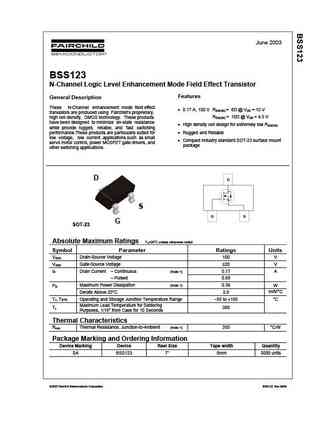
June 2003 BSS123 N-Channel Logic Level Enhancement Mode Field Effect Transistor Features General Description These N-Channel enhancement mode field effect 0.17 A, 100 V. RDS(ON) = 6 @ VGS = 10 V transistors are produced using Fairchild s proprietary, RDS(ON) = 10 @ VGS = 4.5 V high cell density, DMOS technology. These products have been designed to minimize on-state resist... See More ⇒
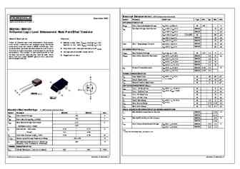
EI ectri caI Characteri sti cs(TA = 25 C unl ess ot herwi se not ed) Sept ember 1996 Symb I Parameter C ndi ti ns Type Min Typ Max Units OFF CHARACTERI STI CS BVDSS Drai n- Source Breakdown Vol t age VGS = 0 V, ID= 250 A All 100 V BSS100 IDSS Zero Gat e Vol t age Drai n Current VDS = 100 V,VGS= 0 V 15 A BSS100 / BSS123 VDS = 100 V,VGS= 0 V BSS123 1 A N ChanneI L gi c LeveI... See More ⇒
Important notice Dear Customer, On 7 February 2017 the former NXP Standard Product business became a new company with the tradename Nexperia. Nexperia is an industry leading supplier of Discrete, Logic and PowerMOS semiconductors with its focus on the automotive, industrial, computing, consumer and wearable application markets In data sheets and application notes which still contain... See More ⇒
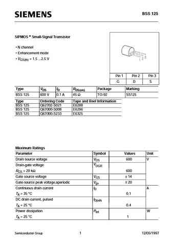
BSS 125 SIPMOS Small-Signal Transistor N channel Enhancement mode VGS(th) = 1.5 ...2.5 V Pin 1 Pin 2 Pin 3 G D S Type VDS ID RDS(on) Package Marking BSS 125 600 V 0.1 A 45 TO-92 SS125 Type Ordering Code Tape and Reel Information BSS 125 Q62702-S021 E6288 BSS 125 Q67000-S008 E6296 BSS 125 Q67000-S233 E6325 Maximum Ratings Parameter Symbol Values Unit Drain sourc... See More ⇒
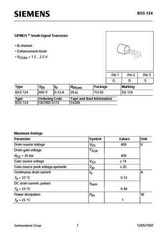
BSS 124 SIPMOS Small-Signal Transistor N channel Enhancement mode VGS(th) = 1.5 ...2.5 V Pin 1 Pin 2 Pin 3 G D S Type VDS ID RDS(on) Package Marking BSS 124 400 V 0.12 A 28 TO-92 SS 124 Type Ordering Code Tape and Reel Information BSS 124 Q67000-S172 E6288 Maximum Ratings Parameter Symbol Values Unit Drain source voltage VDS 400 V VDGR Drain-gate voltage RGS =... See More ⇒
BSS123WQ N-CHANNEL ENHANCEMENT MODE MOSFET Product Summary Features and Benefits ID Low Gate Threshold Voltage V(BR)DSS RDS(ON) TA = +25 C Low Input Capacitance 100V 170mA 6.0 @ VGS = 10V Fast Switching Speed Low Input/Output Leakage High Drain-Source Voltage Rating Description Totally Lead-Free & Fully RoHS compliant (Notes 1 & 2) Hal... See More ⇒
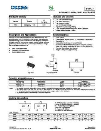
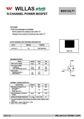
BSS123 N-CHANNEL ENHANCEMENT MODE FIELD EFFECT TRANSISTOR Please click here to visit our online spice models database. Features Mechanical Data Low Gate Threshold Voltage Case SOT-23 Low Input Capacitance Case Material Molded Plastic. UL Flammability Classification Rating 94V-0 Fast Switching Speed Moisture Sensitivity Level 1 per J-STD-020C Low In... See More ⇒
BSS127 N-CHANNEL ENHANCEMENT MODE FIELD MOSFET Product Summary Features ID Low Input Capacitance BVDSS RDS(ON) Package TA = +25 C High BVDSS Rating for Power Application SC59 Low Input/Output Leakage 600V 160 @ VGS = 10V 70mA SOT23 Totally Lead-Free & Fully RoHS Compliant (Notes 1 & 2) Halogen and Antimony Free. Green Device (Note 3) Des... See More ⇒
BSS123 N-CHANNEL ENHANCEMENT MODE MOSFET Product Summary Features and Benefits Low Gate Threshold Voltage ID V(BR)DSS RDS(ON) Low Input Capacitance TA = 25 C Fast Switching Speed 100V 6.0 @ VGS = 10V 0.17 Low Input/Output Leakage High Drain-Source Voltage Rating Lead, Halogen and Antimony Free, RoHS Compliant "Green" Device (Notes 1 and 2... See More ⇒
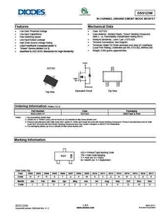
BSS123W N-CHANNEL ENHANCEMENT MODE MOSFET Features Mechanical Data Low Gate Threshold Voltage Case SOT323 Low Input Capacitance Case Material Molded Plastic, "Green" Molding Compound, Note 3. UL Flammability Classification Rating 94V-0 Fast Switching Speed Moisture Sensitivity Level 1 per J-STD-020 Low Input/Output Leakage Terminal Connections ... See More ⇒
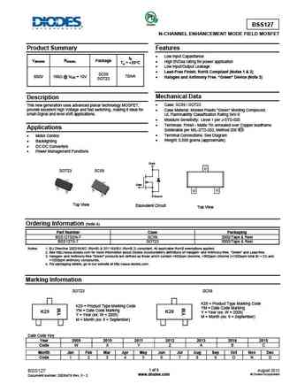
Green BSS127 N-CHANNEL ENHANCEMENT MODE FIELD MOSFET Product Summary Features Low Input Capacitance ID V(BR)DSS RDS(ON) Package High BVDss rating for power application TA = +25 C Low Input/Output Leakage Lead-Free Finish; RoHS Compliant (Notes 1 & 2) SC59 600V 160 @ VGS = 10V 70mA Halogen and Antimony Free. Green Device (Note 3) SOT23 Me... See More ⇒
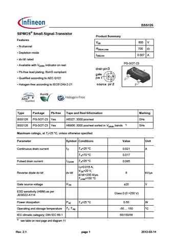
BSS126 SIPMOS Small-Signal-Transistor Product Summary Features VDS 600 V N-channel RDS(on),max 700 Depletion mode IDSS,min 0.007 A dv /dt rated PG-SOT-23 Available with VGS(th) indicator on reel Pb-free lead plating; RoHS compliant Qualified according to AEC Q101 Halogen-free according to IEC61249-2-21 Type Package Pb-free Tape and Reel Informati... See More ⇒
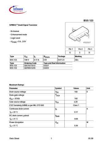
BSS 123 SIPMOS Small-Signal Transistor N channel Enhancement mode Logic Level VGS(th) = 0.8...2.0V Pin 1 Pin 2 Pin 3 G S D Type VDS ID RDS(on) Package Marking BSS 123 100 V 0.17 A 6 SOT-23 SAs Type Ordering Code Tape and Reel Information BSS 123 Q62702-S512 E6327 BSS 123 Q67000-S245 E6433 Maximum Ratings Parameter Symbol Values Unit Drain source voltage VDS... See More ⇒
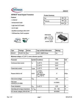
Type BSS127 SIPMOS Small-Signal-Transistor Product Summary Features V 600 V DS n-channel R 500 DS(on),max enhancement mode I 0.021 A D Logic level (4.5V rated) dv /dt rated Qualified according to AEC Q101 PG-SOT-23 100%lead-free; RoHS compliant Type Package Pb-free Tape and Reel Information Marking BSS127 PG-SOT-23 Yes L6327 3000PCS/reel Sis M... See More ⇒
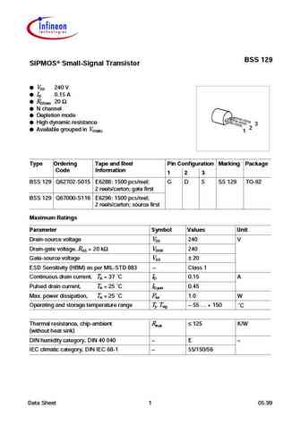
BSS 129 SIPMOS Small-Signal Transistor VDS 240 V ID 0.15 A RDS(on) 20 N channel Depletion mode High dynamic resistance 3 2 Available grouped in VGS(th) 1 Type Ordering Tape and Reel Pin Configuration Marking Package Code Information 1 2 3 BSS 129 Q62702-S015 E6288 1500 pcs/reel; G D S SS 129 TO-92 2 reels/carton; gate first BSS 129 Q67000-S116 E6296 1500 pcs/ree... See More ⇒
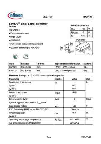
Rev. 1.41 BSS123 SIPMOS Small-Signal-Transistor Product Summary Feature VDS 100 V N-Channel RDS(on) 6 Enhancement mode ID 0.17 A Logic Level PG-SOT23 dv/dt rated 3 Drain pin 3 Gate Qualified according to AEC Q101 pin1 2 Source pin 2 1 VPS05161 Type Package Pb-free Tape and Reel Information Marking PG-SOT23 Yes BSS123 L6327 3000 pcs/reel SAs ... See More ⇒
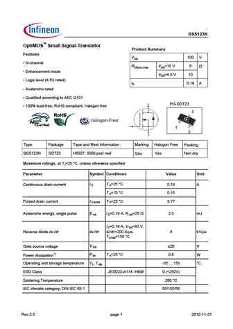
BSS123N OptiMOS Small-Signal-Transistor Product Summary Features VDS 100 V N-channel RDS(on),max VGS=10 V 6 W Enhancement mode VGS=4.5 V 10 Logic level (4.5V rated) ID 0.19 A Avalanche rated Qualified according to AEC Q101 PG-SOT23 100% lead-free; RoHS compliant, Halogen free 3 1 2 Marking Type Package Tape and Reel Information Halogon F... See More ⇒
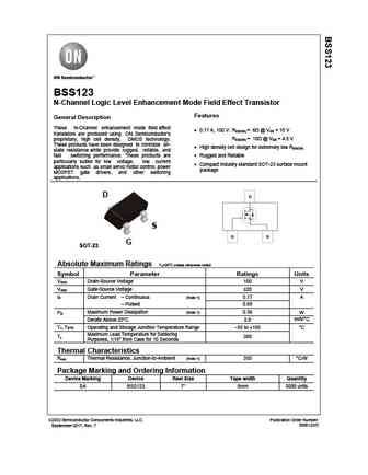
BSS123 N-Channel Logic Level Enhancement Mode Field Effect Transistor Features General Description These N-Channel enhancement mode field effect 0.17 A, 100 V. RDS(ON) = 6 @ VGS = 10 V transistors are produced using ON Semiconductor s RDS(ON) = 10 @ VGS = 4.5 V proprietary, high cell density, DMOS technology. These products have been designed to minimize on- High de... See More ⇒
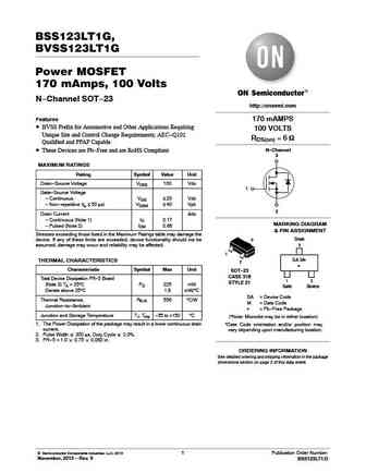
BSS123LT1G, BVSS123LT1G Power MOSFET 170 mAmps, 100 Volts N-Channel SOT-23 http //onsemi.com Features 170 mAMPS BVSS Prefix for Automotive and Other Applications Requiring 100 VOLTS Unique Site and Control Change Requirements; AEC-Q101 RDS(on) = 6 W Qualified and PPAP Capable N-Channel These Devices are Pb-Free and are RoHS Compliant 3 MAXIMUM RATINGS Rating Symbol Value... See More ⇒
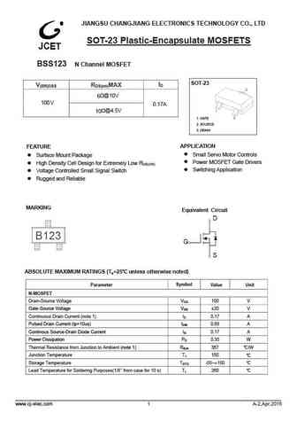
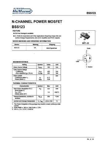
JIANGSU CHANGJIANG ELECTRONICS TECHNOLOGY CO., LTD SOT-23 Plastic-Encapsulate MOSFETS BSS123 N Channel MOSFET SOT-23 ID V(BR)DSS RDS(on)MAX 6 @10V 100V 0.17A @4.5V 10 1. GATE 2. SOURCE 3. DRAIN APPLICATION FEATURE Small Servo Motor Controls Surface Mount Package Power MOSFET Gate Drivers High Density Cell Design for Extremely Low RDS... See More ⇒
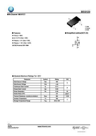
BSS123 N-Channel MOSFET 3 2 1. Gate 2. Source 1 3. Drain Features Simplified outline(SOT-23) VDS (V) =100V D ID =0.17 A(VGS = 10V) RDS(ON) 6 (VGS =10V) RDS(ON) 10 (VGS =4.5V) ESD Protected 2KV HBM G S Absolute Maximum Ratings Ta = 25 Parameter Symbol Rating Unit Drain-Source Voltage VDS 100 V Gate-Source Voltage VGS 20 Continuous Drain Current ID 0.17 A Pulsed Dr... See More ⇒
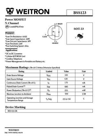
BSS123 Power MOSFET N-Channel 3 DRAIN SOT-23 Features 3 1 *Low On-Resistance 6.0 GATE 1 *Low Input Capacitance 20PF 2 *Low Out put Capacitance 9PF 2 SOURCE *Low Threshole 2.8V *Fast Switching Speed 20ns Application * DC to DC Converter * Cellular & PCMCIA Card * Cordless Telephone * Power Management in Portable and Battery etc. Maximum Ratings (TA=25 C Unles... See More ⇒
FM120-M WILLAS THRU BSS123LT1 FM1200-M 1.0A SURFACE MOUNT SCHOTTKY BARRIER RECTIFIERS -20V- 200V N-CHANNEL POWER MOSFET SOD-123 PACKAGE Pb Free Product Package outline Features Batch process design, excellent power dissipation offers better reverse leakage current and thermal resistance. SOD-123H Low profile surface mounted application in order to optimize board s... See More ⇒
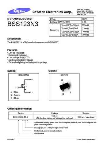
Spec. No. C580N3 Issued Date 2011.09.16 CYStech Electronics Corp. Revised Date 2018.06.20 Page No. 1/8 N-CHANNEL MOSFET BVDSS 100V ID@VGS=10V, TA=25 C 1.7A 290m BSS123N3 VGS=10V, ID=700mA 310m VGS=4V, ID=400mA RDSON(TYP) 260m VGS=10V, ID=170mA 280m VGS=4V, ID=170mA Description The BSS123N3 is a N-channel enhancement-mode MOSFET. Features ... See More ⇒
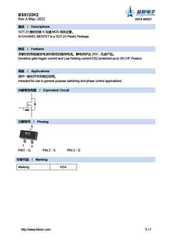
BSS123K2 Rev.A May.-2022 DATA SHEET / Descriptions SOT-23 N MOS N-CHANNEL MOSFET in a SOT-23 Plastic Package. / Features 2KV Sensitive gate trigger current and Low Holding current.ESD protected up to 2KV,HF Product. / Applications ... See More ⇒
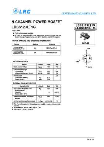
LESHAN RADIO COMPANY, LTD. N-CHANNEL POWER MOSFET LBSS123LT1G LBSS123LT1G S-LBSS123LT1G FEATURE 3 Pb-Free Package is available. S- Prefix for Automotive and Other Applications Requiring Unique Site and Control Change Requirements; AEC-Q101 Qualified and PPAP Capable. 1 DEVICE MARKING AND ORDERING INFORMATION 2 SOT-23 Device Marking Shipping LBSS123LT1G 3000/Tape&Reel SA ... See More ⇒
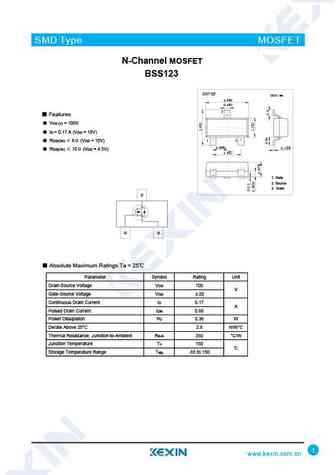
SMD Type MOSFET N-Channel MOSFET BSS123 SOT-23 Unit mm +0.1 2.9 -0.1 +0.1 0.4 -0.1 3 Features VDS (V) = 100V ID = 0.17 A (VGS = 10V) 1 2 RDS(ON) 6 (VGS = 10V) +0.1 +0.05 0.95 -0.1 0.1-0.01 RDS(ON) 10 (VGS = 4.5V) +0.1 1.9 -0.1 1. Gate 2. Source 3. Drain D G S Absolute Maximum Ratings Ta = 25 Parameter Symbol Rating Unit D... See More ⇒
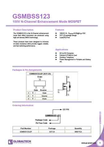
GSMBSS123 100V N-Channel Enhancement Mode MOSFET Product Description Features The GSMBSS123 is the N-Channel enhancement 100V/0.1A , RDS(ON)=6.0 @VGS=10V mode field effect transistors are produced using SOT-23 package design high cell density DMOS technology. Lead(Pb)-Free These products have been designed to minimize on-state resistance while provide rugged, reliable, and... See More ⇒
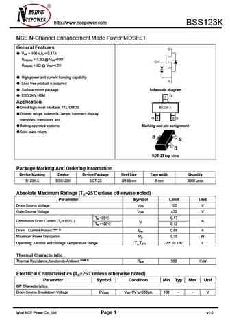
http //www.ncepower.com BSS123K NCE N-Channel Enhancement Mode Power MOSFET General Features VDS = 100 V,ID = 0.17A RDS(ON) ... See More ⇒
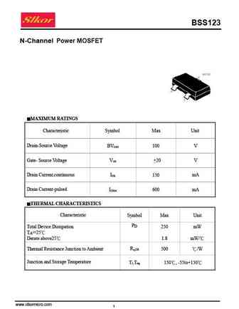
BSS123 N-Channel Power MOSFET MAXIMUM RATINGS Characteristic Symbol Max Unit Drain-Source Voltage BV 100 V DSS Gate- Source Voltage V +20 V GS Drain Current-continuous I 150 mA DR Drain Current-pulsed I 600 mA DRM THERMAL CHARACTERISTICS Characteristic Symbol Max Unit PD Total Device Dissipation 250 mW TA=25 Derate above25 1.8 mW/ R Thermal Resistance Junct... See More ⇒
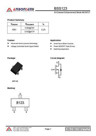
BSS123 N-Channel Enhancement Mode MOSFET Product Summary V(BR)DSS RDS(on)MAX ID 5.0 @10V 100V 0.2A 5.5 @4.5V Feature Application Advanced trench process technology Small Servo Motor Controls Voltage Controlled Small Signal Switch Power MOSFET Gate Drivers Switching Application Package Circuit diagram SOT-23 Marking B123. Document ID Issued Date Revised Date Re... See More ⇒
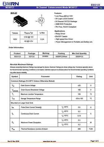
BSS123 MOSFET ROHS N-Channel Enhancement-Mode MOSFET SOT-23 - Features Low RDS(on) @VGS=10V 5V Logic Level Control N Channel SOT23 Package HMB ESD Protection Pb-Free, RoHS Compliant Applications V R Typ I Max (BR)DSS DS(ON) D Relay Driver ON/OFF Switch 3.5 @ 10V 100V 0.2A High-speed line Driver 4 @ 4.5V Power Management in Portab... See More ⇒
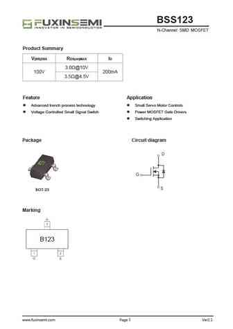
BSS123 N-Channel SMD MOSFET Product Summary V R I (BR)DSS DS(on)MAX D 3.0 @10V 100V 200mA 3.5 @4.5V Feature Application Advanced trench process technology Small Servo Motor Controls Voltage Controlled Small Signal Switch Power MOSFET Gate Drivers Switching Application Package Circuit diagram SOT-23 Marking B123 www.fuxinsemi.com Page 1 Ver2.1 BSS123 N-Ch... See More ⇒
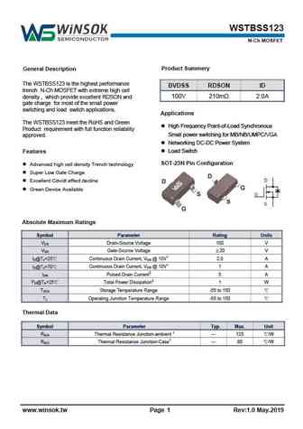
WSTBSS123 N-Ch MOSFET Product Summery General Description The WSTBSS123 is the highest performance BVDSS RDSON ID trench N-Ch MOSFET with extreme high cell 100V 210m 2.0A density , which provide excellent RDSON and gate charge for most of the small power switching and load switch applications. Applications The WSTBSS123 meet the RoHS and Green High Frequency Point-of-L... See More ⇒
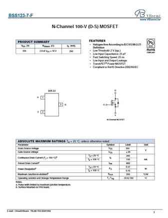
BSS123-7-F www.VBsemi.tw N-Channel 100-V (D-S) MOSFET FEATURES PRODUCT SUMMARY Halogen-free According to IEC 61249-2-21 VDS (V) RDS(on) ( )ID (mA) Definition 100 2.8 at VGS = 10 V Low Threshold 2 V (typ.) 260 Low Input Capacitance 25 pF Fast Switching Speed 25 ns Low Input and Output Leakage TrenchFET Power MOSFET Compliant to RoHS Directive 200... See More ⇒
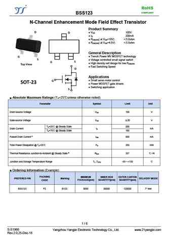
RoHS COMPLIANT BSS123 N-Channel Enhancement Mode Field Effect Transistor Product Summary V 100V DS I 200mA D R ( at V =10V) 5.0ohm DS(ON) GS R ( at V =4.5V) 5.5ohm DS(ON) GS General Description Trench Power MV MOSFET technology Voltage controlled small signal switch High density cell design for low R DS(ON) Fast Switching Spe... See More ⇒
BSS123 N-CHANNEL POWER MOSFET BSS123 FEATURE 3 Pb-Free Package is available. S- Prefix for Automotive and Other Applications Requiring Unique Site and Control Change Requirements; AEC-Q101 Qualified and PPAP Capable. 1 DEVICE MARKING AND ORDERING INFORMATION 2 SOT-23 Device Marking Shipping BSS123 SA 3000/Tape&Reel Drain 3 . 1 Gate MAXIMUM RATINGS Rating Symbol Value... See More ⇒
Detailed specifications: BSR52, BSR55, BSR59, BSR60, BSR61, BSR62, BSS10, BSS11, 2SD1047, BSS13, BSS14, BSS15, BSS16, BSS17, BSS18, BSS19, BSS20
Keywords - BSS12 pdf specs
BSS12 cross reference
BSS12 equivalent finder
BSS12 pdf lookup
BSS12 substitution
BSS12 replacement
History: BSR14R | LMBT3906WT1G | ZTX968 | 2SC1000 | 2SB1116 | H3619 | 2N6733
🌐 : EN ES РУ

LIST
Last Update
BJT: GA1A4M | SBT42 | 2SA200-Y
Popular searches
9014 transistor | irfp260n datasheet | irfp250m | 2sk1058 | ss8550 | mje15033 | 2sc945 datasheet | a92 transistor