C63 Specs and Replacement
Type Designator: C63
Material of Transistor: Si
Polarity: NPN
Absolute Maximum Ratings
Maximum Collector Power Dissipation (Pc): 0.36 W
Maximum Collector-Base Voltage |Vcb|: 50 V
Maximum Collector-Emitter Voltage |Vce|: 35 V
Max. Operating Junction Temperature (Tj): 175 °C
Electrical Characteristics
Transition Frequency (ft): 250 MHz
Collector Capacitance (Cc): 3 pF
Forward Current Transfer Ratio (hFE), MIN: 35
Package: TO18
C63 Substitution
- BJT ⓘ Cross-Reference Search
C63 datasheet
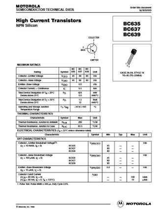
MOTOROLA Order this document SEMICONDUCTOR TECHNICAL DATA by BC635/D High Current Transistors BC635 NPN Silicon BC637 BC639 COLLECTOR 2 3 BASE 1 EMITTER 1 MAXIMUM RATINGS 2 3 BC BC BC 635 637 639 Rating Symbol Unit CASE 29 04, STYLE 14 TO 92 (TO 226AA) Collector Emitter Voltage VCEO 45 60 80 Vdc Collector Base Voltage VCBO 45 60 80 Vdc Emitter Base Voltage ... See More ⇒
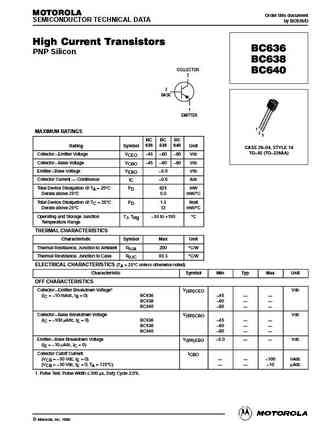
MOTOROLA Order this document SEMICONDUCTOR TECHNICAL DATA by BC636/D High Current Transistors BC636 PNP Silicon BC638 COLLECTOR BC640 2 3 BASE 1 EMITTER 1 MAXIMUM RATINGS 2 3 BC BC BC 636 638 640 Rating Symbol Unit CASE 29 04, STYLE 14 TO 92 (TO 226AA) Collector Emitter Voltage VCEO 45 60 80 Vdc Collector Base Voltage VCBO 45 60 80 Vdc Emitt... See More ⇒
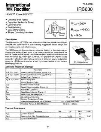
PD- 96003B IRC630PbF Lead-Free www.irf.com 1 2/10/05 IRC630PbF 2 www.irf.com IRC630PbF www.irf.com 3 IRC630PbF 4 www.irf.com IRC630PbF www.irf.com 5 IRC630PbF 6 www.irf.com IRC630PbF www.irf.com 7 IRC630PbF 8 www.irf.com IRC630PbF HexsenseTO-220 5L Package Outline ( Dimensions are shown in millimeters (inches) Hexsense TO-220 5L Part Marking Information EXAMP... See More ⇒

DISCRETE SEMICONDUCTORS DATA SHEET book, halfpage M3D186 BC635; BC637; BC639 NPN medium power transistors Product specification 2001 Oct 10 Supersedes data of 1999 Apr 23 Philips Semiconductors Product specification NPN medium power transistors BC635; BC637; BC639 FEATURES PINNING High current (max. 1 A) PIN DESCRIPTION Low voltage (max. 80 V). 1 base 2 collector APPLIC... See More ⇒
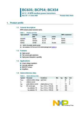
BC635; BCP54; BCX54 45 V, 1 A NPN medium power transistors Rev. 07 4 June 2007 Product data sheet 1. Product profile 1.1 General description NPN medium power transistor series. Table 1. Product overview Type number[1] Package PNP complement NXP JEITA JEDEC BC635[2] SOT54 SC-43A TO-92 BC636 BCP54 SOT223 SC-73 - BCP51 BCX54 SOT89 SC-62 TO-243 BCX51 [1] Valid for all available sele... See More ⇒
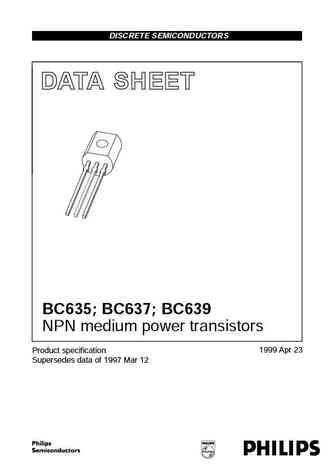
DISCRETE SEMICONDUCTORS DATA SHEET book, halfpage M3D186 BC635; BC637; BC639 NPN medium power transistors 1999 Apr 23 Product specification Supersedes data of 1997 Mar 12 Philips Semiconductors Product specification NPN medium power transistors BC635; BC637; BC639 FEATURES PINNING High current (max. 1 A) PIN DESCRIPTION Low voltage (max. 80 V). 1 base 2 collector APPLI... See More ⇒
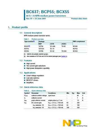
BC637; BCP55; BCX55 60 V, 1 A NPN medium power transistors Rev. 07 25 June 2007 Product data sheet 1. Product profile 1.1 General description NPN medium power transistor series. Table 1. Product overview Type number[1] Package PNP complement NXP JEITA JEDEC BC637[2] SOT54 SC-43A TO-92 BC638 BCP55 SOT223 SC-73 - BCP52 BCX55 SOT89 SC-62 TO-243 BCX52 [1] Valid for all available sel... See More ⇒
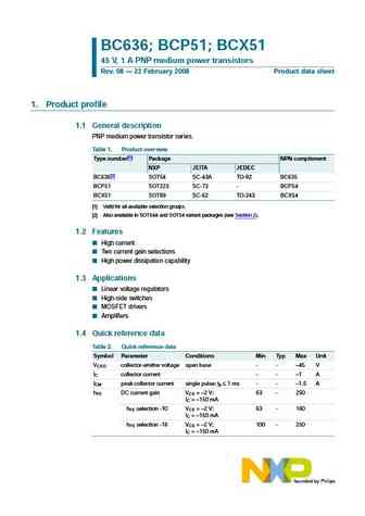
BC636; BCP51; BCX51 45 V, 1 A PNP medium power transistors Rev. 08 22 February 2008 Product data sheet 1. Product profile 1.1 General description PNP medium power transistor series. Table 1. Product overview Type number[1] Package NPN complement NXP JEITA JEDEC BC636[2] SOT54 SC-43A TO-92 BC635 BCP51 SOT223 SC-73 - BCP54 BCX51 SOT89 SC-62 TO-243 BCX54 [1] Valid for all available... See More ⇒

BC639; BCP56; BCX56 80 V, 1 A NPN medium power transistors Rev. 08 22 June 2007 Product data sheet 1. Product profile 1.1 General description NPN medium power transistor series. Table 1. Product overview Type number[1] Package PNP complement NXP JEITA JEDEC BC639[2] SOT54 SC-43A TO-92 BC640 BCP56 SOT223 SC-73 - BCP53 BCX56 SOT89 SC-62 TO-243 BCX53 [1] Valid for all available sel... See More ⇒

DISCRETE SEMICONDUCTORS DATA SHEET book, halfpage M3D186 BC636; BC638; BC640 PNP medium power transistors 1999 Apr 23 Product specification Supersedes data of 1997 Mar 07 Philips Semiconductors Product specification PNP medium power transistors BC636; BC638; BC640 FEATURES PINNING High current (max. 1 A) PIN DESCRIPTION Low voltage (max. 80 V). 1 base 2 collector APPLI... See More ⇒
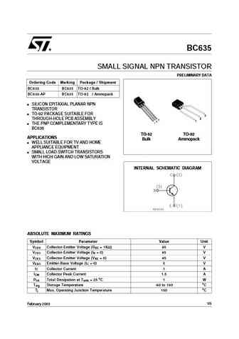
BC635 SMALL SIGNAL NPN TRANSISTOR PRELIMINARY DATA Ordering Code Marking Package / Shipment BC635 BC635 TO-92 / Bulk BC635-AP BC635 TO-92 / Ammopack SILICON EPITAXIAL PLANAR NPN TRANSISTOR TO-92 PACKAGE SUITABLE FOR THROUGH-HOLE PCB ASSEMBLY THE PNP COMPLEMENTARY TYPE IS BC636 TO-92 TO-92 APPLICATIONS Bulk Ammopack WELL SUITABLE FOR TV AND HOME APPLIANCE EQUIPMENT SMA... See More ⇒
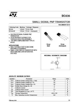
BC636 SMALL SIGNAL PNP TRANSISTOR PRELIMINARY DATA Ordering Code Marking Package / Shipment BC636 BC636 TO-92 / Bulk BC636-AP BC636 TO-92 / Ammopack SILICON EPITAXIAL PLANAR PNP TRANSISTOR TO-92 PACKAGE SUITABLE FOR THROUGH-HOLE PCB ASSEMBLY THE NPN COMPLEMENTARY TYPE IS BC635 TO-92 TO-92 APPLICATIONS Bulk Ammopack WELL SUITABLE FOR TV AND HOME APPLIANCE EQUIPMENT SMA... See More ⇒
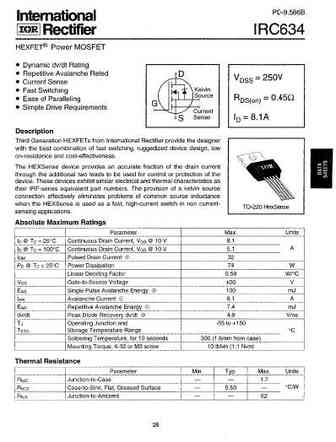
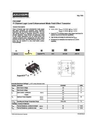
June1996 NDC632P P-Channel Logic Level Enhancement Mode Field Effect Transistor General Description Features These P-Channel logic level enhancement mode -2.7A, -20V. RDS(ON) = 0.14 @ VGS = -4.5V power field effect transistors are produced using RDS(ON) = 0.2 @ VGS = -2.7V. Fairchild's proprietary, high cell density, DMOS technology. This very high density process is Propriet... See More ⇒
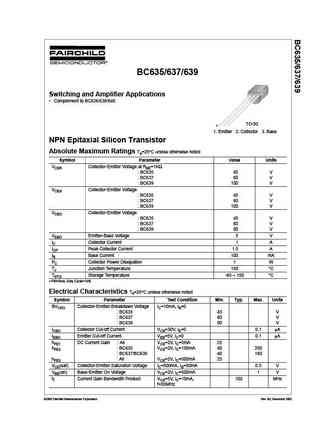
BC635/637/639 Switching and Amplifier Applications Complement to BC636/638/640 TO-92 1 1. Emitter 2. Collector 3. Base NPN Epitaxial Silicon Transistor Absolute Maximum Ratings Ta=25 C unless otherwise noted Symbol Parameter Value Units VCER Collector-Emitter Voltage at RBE=1K BC635 45 V BC637 60 V BC639 100 V VCES Collector-Emitter Voltage BC635 45 V BC637 6... See More ⇒
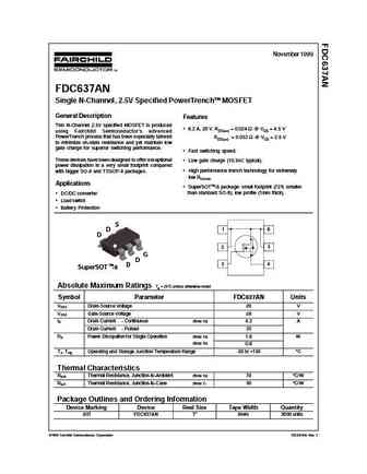
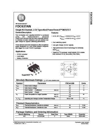
November 1999 FDC637AN Single N-Channel, 2.5V Specified PowerTrenchTM MOSFET General Description Features This N-Channel 2.5V specified MOSFET is produced 6.2 A, 20 V. RDS(on) = 0.024 @ VGS = 4.5 V using Fairchild Semiconductor's advanced PowerTrench process that has been especially tailored RDS(on) = 0.032 @ VGS = 2.5 V to minimize on-state resistance and yet maintain lo... See More ⇒
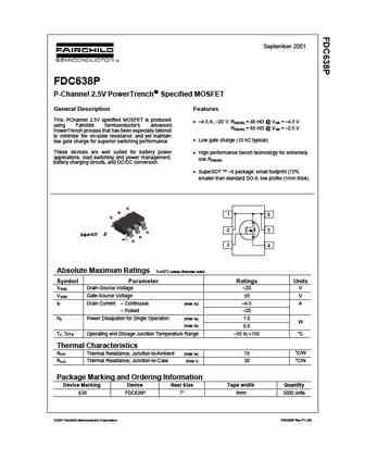
September 2001 FDC638P P-Channel 2.5V PowerTrench Specified MOSFET General Description Features This P 2.5V specified MOSFET is produced -Channel 4.5 A, 20 V. R = 48 m @ V = 4.5 V DS(ON) GS using Fairchild Semiconductor s advanced R = 65 m @ V = 2.5 V DS(ON) GS PowerTrench process that has been especially tailored to minimize the on-state resistanc... See More ⇒
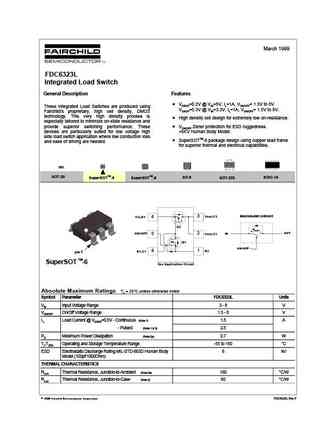
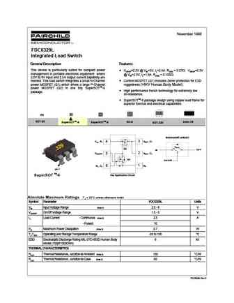
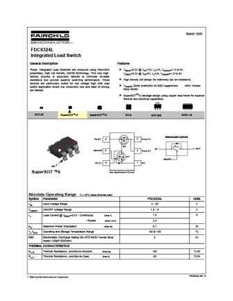
March 1999 FDC6323L Integrated Load Switch General Description Features VDROP=0.2V @ VIN=5V, IL=1A, VON/OFF= 1.5V to 8V These Integrated Load Switches are produced using VDROP=0.3V @ VIN=3.3V, IL=1A, VON/OFF= 1.5V to 8V. Fairchild's proprietary, high cell density, DMOS technology. This very high density process is High density cell design for extremely low on-resistance. especially... See More ⇒
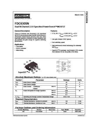
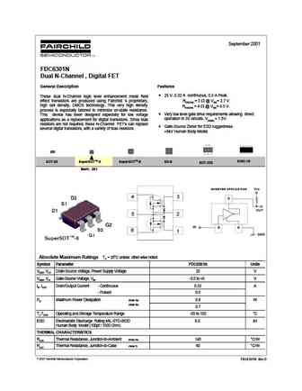
March 1999 FDC6305N Dual N-Channel 2.5V Specified PowerTrenchTM MOSFET General Description Features 2.7 A, 20 V. RDS(ON) = 0.08 @ VGS = 4.5 V These N-Channel low threshold 2.5V specified MOSFETs are produced using Fairchild Semiconductor's RDS(ON) = 0.12 @ VGS = 2.5 V advanced PowerTrench process that has been especially tailored to minimize on-state resistance and Low... See More ⇒
BC63916 Switching and Amplifier Applications TO-92 1 1. Emitter 2. Collector 3. Base NPN Epitaxial Silicon Transistor Absolute Maximum Ratings Ta=25 C unless otherwise noted Symbol Parameter Value Units VCER Collector-Emitter Voltage at RBE=1K 100 V VCES Collector-Emitter Voltage 100 V VCEO Collector-Emitter Voltage 80 V VEBO Emitter-Base Voltage 5 V IC Collector Current 1 A P... See More ⇒
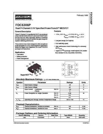
February 1999 FDC6306P Dual P-Channel 2.5V Specified PowerTrench MOSFET Features General Description These P-Channel 2.5V specified MOSFETs are produced -1.9 A, -20 V. RDS(on) = 0.170 @ VGS = -4.5 V using Fairchild Semiconductor's advanced PowerTrench RDS(on) = 0.250 @ VGS = -2.5 V process that has been especially tailored to minimize on-state resistance and yet maintain... See More ⇒
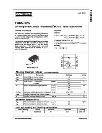
April 2002 FDC6392S 20V Integrated P-Channel PowerTrench MOSFET and Schottky Diode General Description Features MOSFET The FDC6392S combines the exceptional performance of Fairchild's PowerTrench MOSFET technology with a 2.2 A, 20V. RDS(ON) = 150 m @ VGS = 4.5V very low forward voltage drop Schottky barrier rectifier RDS(ON) = 200 m @ VGS... See More ⇒
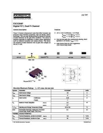
July 1997 FDC6304P Digital FET, Dual P-Channel General Description Features -25 V, -0.46 A continuous, -1.0 A Peak. These P-Channel enhancement mode field effect transistor are produced using Fairchild's proprietary, high cell density, DMOS RDS(ON) = 1.5 @ VGS= -2.7 V technology. This very high density process is tailored to minimize RDS(ON) = 1.1 @ VGS = -4.5 V. on-state ... See More ⇒
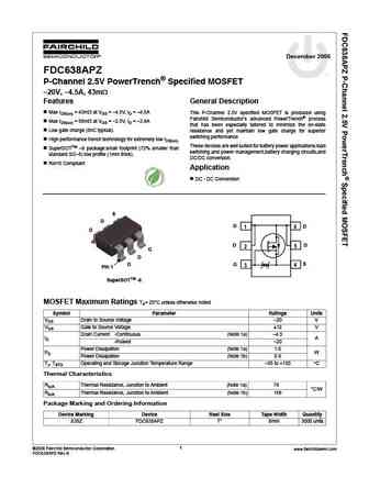
December 2006 FDC638APZ P-Channel 2.5V PowerTrench Specified MOSFET 20V, 4.5A, 43m Features General Description Max rDS(on) = 43m at VGS = 4.5V, ID = 4.5A This P-Channel 2.5V specified MOSFET is produced using Fairchild Semiconductor s advanced PowerTrench process Max rDS(on) = 68m at VGS = 2.5V, ID = 3.8A that has been especially tailored to minim... See More ⇒
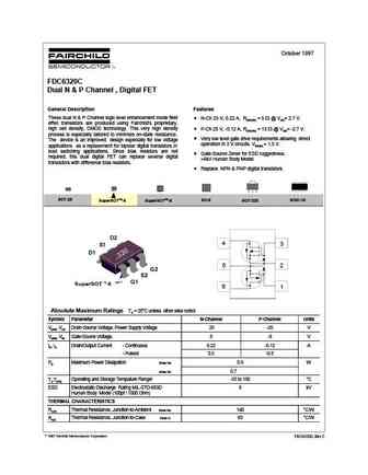
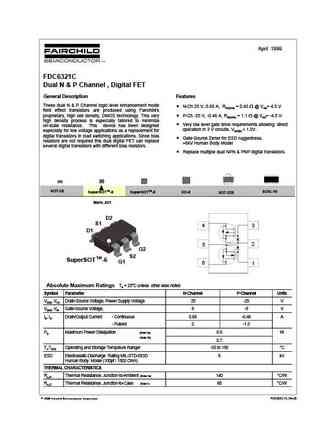
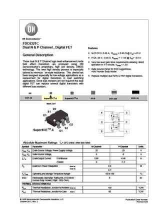
October 1997 FDC6320C Dual N & P Channel , Digital FET General Description Features These dual N & P Channel logic level enhancement mode field N-Ch 25 V, 0.22 A, RDS(ON) = 5 @ VGS= 2.7 V. effec transistors are produced using Fairchild's proprietary, high cell density, DMOS technology. This very high density P-Ch 25 V, -0.12 A, RDS(ON) = 13 @ VGS= -2.7 V. process is especial... See More ⇒
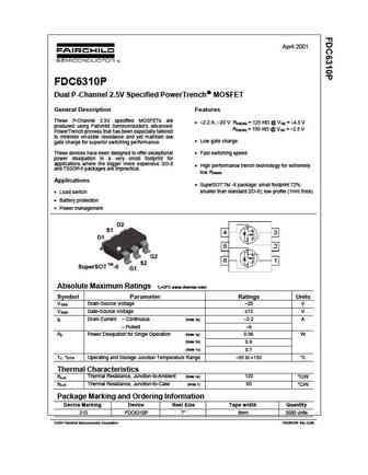
April 2001 FDC6310P Dual P-Channel 2.5V Specified PowerTrench MOSFET General Description Features These P-Channel 2.5V specified MOSFETs are 2.2 A, 20 V. R = 125 m @ V = 4.5 V DS(ON) GS produced using Fairchild Semiconductor's advanced R = 190 m @ V = 2.5 V DS(ON) GS PowerTrench process that has been especially tailored to minimize on-state resistance ... See More ⇒
April 1999 FDC6321C Dual N & P Channel , Digital FET General Description Features These dual N & P Channel logic level enhancement mode N-Ch 25 V, 0.68 A, RDS(ON) = 0.45 @ VGS= 4.5 V field effect transistors are produced using Fairchild's proprietary, high cell density, DMOS technology. This very P-Ch -25 V, -0.46 A, RDS(ON) = 1.1 @ VGS= -4.5 V. high density process is especi... See More ⇒
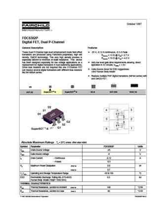
October 1997 FDC6302P Digital FET, Dual P-Channel General Description Features These Dual P-Channel logic level enhancement mode field effect -25 V, -0.12 A continuous, -0.5 A Peak. transistors are produced using Fairchild's proprietary, high cell RDS(ON) = 13 @ VGS= -2.7 V density, DMOS technology. This very high density process is RDS(ON) = 10 @ VGS = -4.5 V. especially... See More ⇒
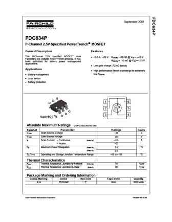
September 2001 FDC634P P-Channel 2.5V Specified PowerTrench MOSFET General Description Features This P-Channel 2.5V specified MOSFET uses 3.5 A, 20 V. R = 80 m @ V = 4.5 V DS(ON) GS Fairchild s low voltage PowerTrench process. It has R = 110 m @ V = 2.5 V DS(ON) GS been optimized for battery power management applications. Low gate charge (7.2 n... See More ⇒
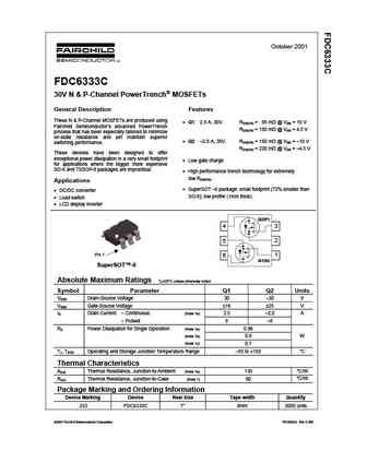
October 2001 FDC6333C 30V N & P-Channel PowerTrench MOSFETs General Description Features These N & P-Channel MOSFETs are produced using Q1 2.5 A, 30V. RDS(ON) = 95 m @ VGS = 10 V Fairchild Semiconductor s advanced PowerTrench RDS(ON) = 150 m @ VGS = 4.5 V process that has been especially tailored to minimize on-state resistance and yet maintain superior Q2 2... See More ⇒
BC636/638/640 Switching and Amplifier Applications Complement to BC635/637/639 TO-92 1 1. Emitter 2. Collector 3. Base PNP Epitaxial Silicon Transistor Absolute Maximum Ratings Ta=25 C unless otherwise noted Symbol Parameter Value Units VCER Collector-Emitter Voltage at RBE=1K BC636 -45 V BC638 -60 V BC640 -100 V VCES Collector-Emitter Voltage BC636 -45 V BC6... See More ⇒
November 1998 FDC6329L Integrated Load Switch General Description Features This device is particularly suited for compact power VDROP=0.2V @ VIN=5V, IL=2.8A. R(ON) = 0.07 VDROP=0.2V management in portable electronic equipment where @ VIN=2.5V, IL=1.9A. R(ON) = 0.105 . 2.5V to 8V input and 2.5A output current capability are needed. This load switch integrates a small N-Channel ... See More ⇒
September 2001 FDC6301N Dual N-Channel , Digital FET General Description Features 25 V, 0.22 A continuous, 0.5 A Peak. These dual N-Channel logic level enhancement mode field effect transistors are produced using Fairchild 's proprietary, RDS(ON) = 5 @ VGS= 2.7 V high cell density, DMOS technology. This very high density RDS(ON) = 4 @ VGS= 4.5 V. process is especially tailo... See More ⇒
July 1999 FDC6308P Dual P-Channel 2.5V Specified PowerTrenchTM MOSFET General Description Features This P-Channel 2.5V specified MOSFET is a rugged -1.7 A, -18 V. RDS(ON) = 0.18 @ VGS = -4.5 V gate version of Fairchild Semiconductor's advanced RDS(ON) = 0.30 @ VGS = -2.5 V PowerTrench process. It has been optimized for power management applications with a wide range of gate ... See More ⇒
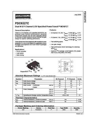
July 2000 FDC6327C Dual N & P-Channel 2.5V Specified PowerTrenchTM MOSFET Features General Description These N & P-Channel 2.5V specified MOSFETs are N-Channel 2.7A, 20V. RDS(on) = 0.08 @ VGS = 4.5V produced using Fairchild Semiconductor's advanced RDS(on) = 0.12 @ VGS = 2.5V PowerTrench process that has been especially tailored to minimize on-state resistance and yet mainta... See More ⇒
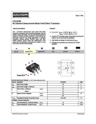
March 1998 FDC633N N-Channel Enhancement Mode Field Effect Transistor General Description Features This N-Channel enhancement mode power field effect 5.2 A, 30 V. RDS(ON) = 0.042 @ VGS = 4.5 V transistors is produced using Fairchild's proprietary, high cell RDS(ON) = 0.054 @ VGS = 2.5 V. density, DMOS technology. This very high density process is tailored to minimize on-stat... See More ⇒
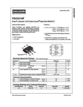
December 2001 FDC6318P Dual P-Channel 1.8V PowerTrench Specified MOSFET General Description Features These P-Channel 1.8V specified MOSFETs are 2.5 A, 12 V. RDS(ON) = 90 m @ VGS = 4.5 V produced using Fairchild Semiconductor's advanced RDS(ON) = 125 m @ VGS = 2.5 V PowerTrench process that has been especially tailored RDS(ON) = 200 m ... See More ⇒

August 1997 FDC6303N Digital FET, Dual N-Channel General Description Features 25 V, 0.68 A continuous, 2 A Peak. These dual N-Channel logic level enhancement mode field RDS(ON) = 0.6 @ VGS = 2.7 V effect transistors are produced using Fairchild's proprietary, high cell density, DMOS technology. This very high density RDS(ON) = 0.45 @ VGS= 4.5 V. process is especially tailored... See More ⇒
May 1998 FDC636P P-Channel Logic Level Enhancement Mode Field Effect Transistor General Description Features These P-Channel logic level enhancement mode power -2.8 A, -20 V. RDS(ON) = 0.130 @ VGS = -4.5 V field effect transistors are produced using Fairchild's RDS(ON) = 0.180 @ VGS = -2.5 V. proprietary, high cell density, DMOS technology. This very high density process is... See More ⇒

March 2009 BC638 PNP Epitaxial Silicon Transistor Switching and Amplifier Applications Complement to BC637 TO-92 1 1. Emitter 2. Collector 3. Base Absolute Maximum Ratings Ta = 25 C unless otherwise noted Symbol Parameter Value Units VCER Collector-Emitter Voltage at RBE=1K -60 V VCES Collector-Emitter Voltage -60 V VCEO Collector-Emitter Voltage -60 V VEBO Emitter-Base Volt... See More ⇒
March 1999 FDC6324L Integrated Load Switch General Description Features These Integrated Load Switches are produced using Fairchild's VDROP=0.2V @ VIN=12V, IL=1A, VON/OFF=1.5 to 8V proprietary, high cell density, DMOS technology. This very high VDROP=0.3V @ VIN=5V, IL=1A, VON/OFF=1.5 to 8V. density process is especially tailored to minimize on-state High density cell design for extr... See More ⇒

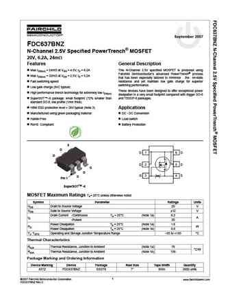
September 2007 FDC637BNZ tm N-Channel 2.5V Specified PowerTrench MOSFET 20V, 6.2A, 24m Features General Description Max rDS(on) = 24m at VGS = 4.5V, ID = 6.2A This N-Channel 2.5V specified MOSFET is produced using Fairchild Semiconductor s advanced PowerTrench process Max rDS(on) = 32m at VGS = 2.5V, ID = 5.2A that has been especially tailored to minimize the on-sta... See More ⇒
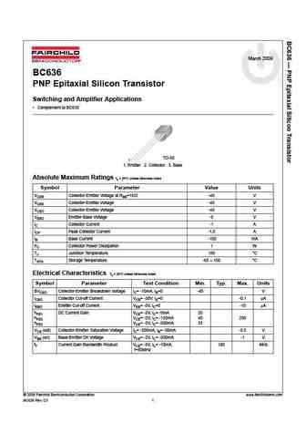
March 2009 BC636 PNP Epitaxial Silicon Transistor Switching and Amplifier Applications Complement to BC635 TO-92 1 1. Emitter 2. Collector 3. Base Absolute Maximum Ratings Ta = 25 C unless otherwise noted Symbol Parameter Value Units VCER Collector-Emitter Voltage at RBE=1K -45 V VCES Collector-Emitter Voltage -45 V VCEO Collector-Emitter Voltage -45 V VEBO Emitter-Base Volt... See More ⇒
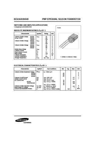
BC636/638/640 PNP EPITAXIAL SILICON TRANSISTOR SWITCHING AND AMPLIFIER APPLICATIONS Complement to BC635/637/639 TO-92 ABSOLUTE MAXIMUM RATINGS (T =25 ) A Characteristic Symbol Rating Unit Collector Emitter Voltage BC636 VCER -45 V at RBE=1Kohm BC638 -60 V BC640 -100 V Collector Emitter Voltage BC636 VCES -45 V BC638 -60 V BC640 -100 V Collector Emitter Voltage BC636 VCE... See More ⇒
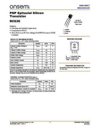
DATA SHEET www.onsemi.com PNP Epitaxial Silicon Transistor TO-92-3 BC636 CASE 135AR Bent Lead 1 2 Features 3 Switching and Amplifier Applications 1. Emitter Complement to BC635 2. Collector These Devices are Pb-Free, Halogen Free/BFR Free and are RoHS 3. Base Compliant MARKING DIAGRAM ABSOLUTE MAXIMUM RATINGS (Values are at TA = 25 C unless otherwise noted) P... See More ⇒

BC637, BC639, BC639-16 High Current Transistors NPN Silicon Features These are Pb-Free Devices* http //onsemi.com COLLECTOR 2 MAXIMUM RATINGS 3 Rating Symbol Value Unit BASE Collector - Emitter Voltage VCEO Vdc BC637 60 1 BC639 80 EMITTER Collector - Base Voltage VCBO Vdc BC637 60 BC639 80 Emitter - Base Voltage VEBO 5.0 Vdc Collector Current - Continuous IC 1.0 Adc TO-... See More ⇒
FDC637AN Single N-Channel, 2.5V Specified PowerTrenchTM MOSFET General Description Features This N-Channel 2.5V specified MOSFET is produced 6.2 A, 20 V. RDS(on) = 0.024 @ VGS = 4.5 V using ON Semiconductor's advanced PowerTrench process that has been especially tailored RDS(on) = 0.032 @ VGS = 2.5 V to minimize on-state resistance and yet maintain low gate charge for ... See More ⇒

Is Now Part of To learn more about ON Semiconductor, please visit our website at www.onsemi.com Please note As part of the Fairchild Semiconductor integration, some of the Fairchild orderable part numbers will need to change in order to meet ON Semiconductor s system requirements. Since the ON Semiconductor product management systems do not have the ability to manage part nomenclatur... See More ⇒
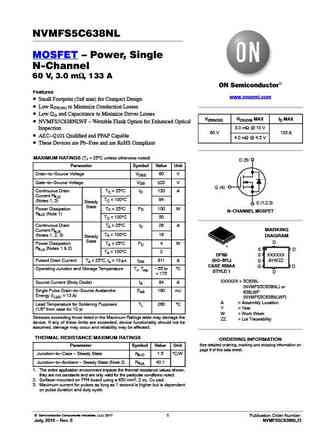
NVMFS5C638NL MOSFET Power, Single N-Channel 60 V, 3.0 mW, 133 A Features www.onsemi.com Small Footprint (5x6 mm) for Compact Design Low RDS(on) to Minimize Conduction Losses Low QG and Capacitance to Minimize Driver Losses V(BR)DSS RDS(ON) MAX ID MAX NVMFS5C638NLWF - Wettable Flank Option for Enhanced Optical 3.0 mW @ 10 V Inspection 60 V 133 A AEC-Q101 Qua... See More ⇒
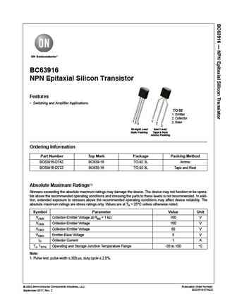
BC63916 NPN Epitaxial Silicon Transistor Features Switching and Amplifier Applications TO-92 1. Emitter 2. Collector 1 1 3. Base 2 2 3 3 Straight Lead Bent Lead Bulk Packing Tape & Reel Ammo Packing Ordering Information Part Number Top Mark Package Packing Method BC63916-D74Z BC639-16 TO-92 3L Ammo BC63916-D27Z BC639-16 TO-92 3L Tape and Reel Absolute Maximum Ratings(1)... See More ⇒

Is Now Part of To learn more about ON Semiconductor, please visit our website at www.onsemi.com Please note As part of the Fairchild Semiconductor integration, some of the Fairchild orderable part numbers will need to change in order to meet ON Semiconductor s system requirements. Since the ON Semiconductor product management systems do not have the ability to manage part nomenclatur... See More ⇒

Is Now Part of To learn more about ON Semiconductor, please visit our website at www.onsemi.com Please note As part of the Fairchild Semiconductor integration, some of the Fairchild orderable part numbers will need to change in order to meet ON Semiconductor s system requirements. Since the ON Semiconductor product management systems do not have the ability to manage part nomenclatur... See More ⇒
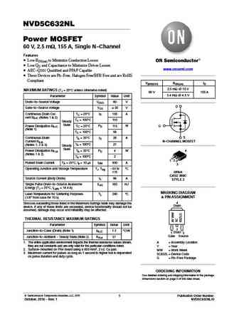
NVD5C632NL Power MOSFET 60 V, 2.5 mW, 155 A, Single N-Channel Features Low RDS(on) to Minimize Conduction Losses Low QG and Capacitance to Minimize Driver Losses www.onsemi.com AEC-Q101 Qualified and PPAP Capable These Devices are Pb-Free, Halogen Free/BFR Free and are RoHS Compliant V(BR)DSS RDS(on) ID 2.5 mW @ 10 V MAXIMUM RATINGS (TJ = 25 C unless otherwise noted... See More ⇒
FDC6321C Dual N & P Channel , Digital FET Features N-Ch 25 V, 0.68 A, RDS(ON) = 0.45 @ VGS= 4.5 V General Description P-Ch -25 V, -0.46 A, RDS(ON) = 1.1 @ VGS= -4.5 V. These dual N & P Channel logic level enhancement mode Very low level gate drive requirements allowing direct field effect transistors are produced using ON operation in 3 V circuits. VGS(th) ... See More ⇒

Is Now Part of To learn more about ON Semiconductor, please visit our website at www.onsemi.com Please note As part of the Fairchild Semiconductor integration, some of the Fairchild orderable part numbers will need to change in order to meet ON Semiconductor s system requirements. Since the ON Semiconductor product management systems do not have the ability to manage part nomenclatur... See More ⇒

BC637, BC639, BC639-16 High Current Transistors NPN Silicon Features These are Pb-Free Devices* http //onsemi.com COLLECTOR 2 MAXIMUM RATINGS 3 Rating Symbol Value Unit BASE Collector - Emitter Voltage VCEO Vdc BC637 60 1 BC639 80 EMITTER Collector - Base Voltage VCBO Vdc BC637 60 BC639 80 Emitter - Base Voltage VEBO 5.0 Vdc Collector Current - Continuous IC 1.0 Adc TO-... See More ⇒

Is Now Part of To learn more about ON Semiconductor, please visit our website at www.onsemi.com Please note As part of the Fairchild Semiconductor integration, some of the Fairchild orderable part numbers will need to change in order to meet ON Semiconductor s system requirements. Since the ON Semiconductor product management systems do not have the ability to manage part nomenclatur... See More ⇒
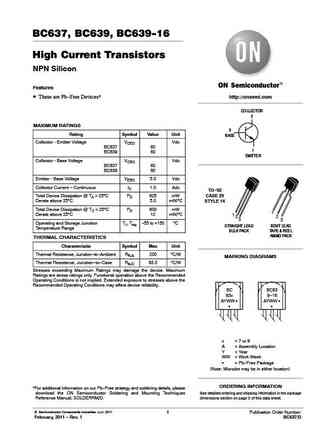
BC637, BC639, BC639-16 High Current Transistors NPN Silicon Features These are Pb-Free Devices* http //onsemi.com COLLECTOR 2 MAXIMUM RATINGS 3 Rating Symbol Value Unit BASE Collector - Emitter Voltage VCEO Vdc BC637 60 1 BC639 80 EMITTER Collector - Base Voltage VCBO Vdc BC637 60 BC639 80 Emitter - Base Voltage VEBO 5.0 Vdc Collector Current - Continuous IC 1.0 Adc TO-... See More ⇒
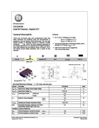
FDC6301N Dual N-Channel , Digital FET Features General Description 25 V, 0.22 A continuous, 0.5 A Peak. These dual N-Channel logic level enhancement mode field RDS(ON) = 5 @ VGS= 2.7 V effect transistors are produced using ON Semiconductor 's RDS(ON) = 4 @ VGS= 4.5 V. proprietary, high cell density, DMOS technology. This very high density process is especially tailored to... See More ⇒

Is Now Part of To learn more about ON Semiconductor, please visit our website at www.onsemi.com ON Semiconductor and the ON Semiconductor logo are trademarks of Semiconductor Components Industries, LLC dba ON Semiconductor or its subsidiaries in the United States and/or other countries. ON Semiconductor owns the rights to a number of patents, trademarks, copyrights, trade secrets, and oth... See More ⇒

Is Now Part of To learn more about ON Semiconductor, please visit our website at www.onsemi.com Please note As part of the Fairchild Semiconductor integration, some of the Fairchild orderable part numbers will need to change in order to meet ON Semiconductor s system requirements. Since the ON Semiconductor product management systems do not have the ability to manage part nomenclatur... See More ⇒
September 2007 FDC637BNZ tm N-Channel 2.5V Specified PowerTrench MOSFET 20V, 6.2A, 24m Features General Description Max rDS(on) = 24m at VGS = 4.5V, ID = 6.2A This N-Channel 2.5V specified MOSFET is produced using Fairchild Semiconductor s advanced PowerTrench process Max rDS(on) = 32m at VGS = 2.5V, ID = 5.2A that has been especially tailored to minimize the on-sta... See More ⇒
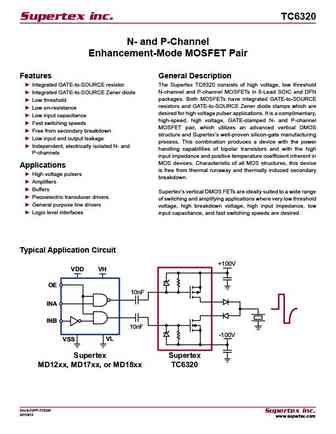
Supertex inc. TC6320 N- and P-Channel Enhancement-Mode MOSFET Pair Features General Description Integrated GATE-to-SOURCE resistor The Supertex TC6320 consists of high voltage, low threshold N-channel and P-channel MOSFETs in 8-Lead SOIC and DFN Integrated GATE-to-SOURCE Zener diode packages. Both MOSFETs have integrated GATE-to-SOURCE Low threshold resistors and GATE-to... See More ⇒
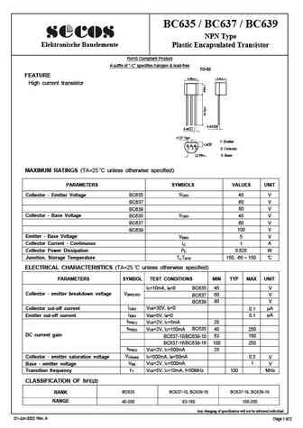
BC635 / BC637 / BC639 NPN Type Elektronische Bauelemente Plastic Encapsulated Transistor RoHS Compliant Product A suffix of "-C" specifies halogen & lead-free TO-92 FEATURE 4.55 0.2 3.5 0.2 High current transistor 08 0.43+0.07 0. 1 0.46+0.1 0. (1.27 Typ. ) 1 Emitter +0.2 1.25 0.2 1 2 3 2 Collector 2.54 0.1 3 Base o MAXIMUM RATINGS (TA=25 C unless otherw... See More ⇒
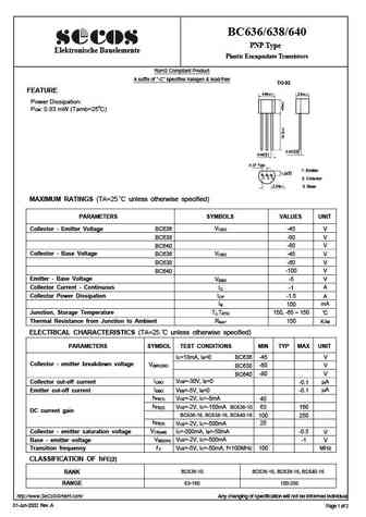
BC636/638/640 PNP Type Elektronische Bauelemente Plastic Encapsulate Transistors RoHS Compliant Product A suffix of "-C" specifies halogen & lead-free TO-92 FEATURE 4.55 0.2 3.5 0.2 Power Dissipation o PCM 0.83 mW (Tamb=25 C) 08 0.43+0.07 0. 1 0.46+0.1 0. (1.27 Typ. ) 1 Emitter +0.2 1.25 0.2 1 2 3 2 Collector 2.54 0.1 3 Base o MAXIMUM RATINGS (TA... See More ⇒
... See More ⇒
... See More ⇒
bc635 bc636 bc637 bc638 bc639 bc640.pdf ![]()
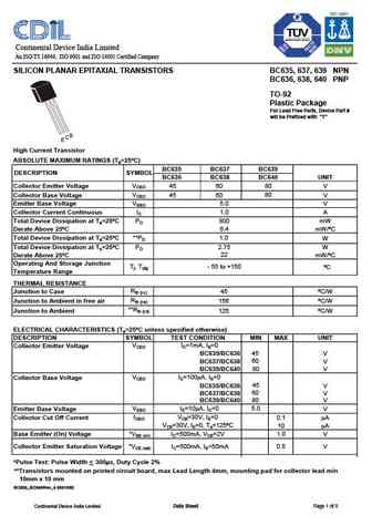
Continental Device India Limited An ISO/TS 16949, ISO 9001 and ISO 14001 Certified Company SILICON PLANAR EPITAXIAL TRANSISTORS BC635, 637, 639 NPN BC636, 638, 640 PNP TO-92 Plastic Package For Lead Free Parts, Device Part # will be Prefixed with "T" B C E High Current Transistor ABSOLUTE MAXIMUM RATINGS (Ta=25 C) BC635 BC637 BC639 DESCRIPTION SYMBOL BC636 BC638 BC640 UNIT VCE... See More ⇒
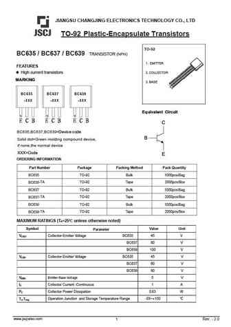
JIANGSU CHANGJING ELECTRONICS TECHNOLOGY CO., LTD TO-92 Plastic-Encapsulate Transistors TO-92 BC635 / BC637 / BC639 TRANSISTOR (NPN) 1. EMITTER FEATURES High current transistors 2. COLLECTOR 3. BASE BC635 BC637 BC639 XXX XXX XXX Equivalent Circuit 1 1 1 BC635,BC637,BC639=Device code Solid dot=Green molding compound device, if none,the normal device XXX=Code... See More ⇒
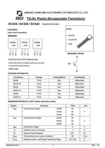
JIANGSU CHANGJING ELECTRONICS TECHNOLOGY CO., LTD TO-92 Plastic-Encapsulate Transistors BC636 / BC638 / BC640 TRANSISTOR (PNP) TO-92 FEATURES High current transistors 1. EMITTER 2. COLLECTOR BC636 BC638 BC640 3. BASE XXX XXX XXX 1 1 1 Equivalent Circuit BC636,BC638,BC640=Device code Solid dot=Green molding compound device, if none,the normal device XXX=Co... See More ⇒

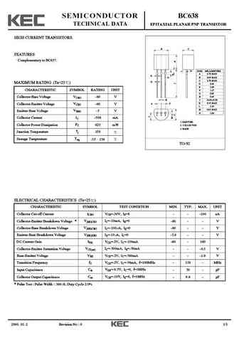
SEMICONDUCTOR BC637 TECHNICAL DATA EPITAXIAL PLANAR NPN TRANSISTOR HIGH CURRENT TRANSISTORS. B C FEATURES Complementary to BC638. N DIM MILLIMETERS A 4.70 MAX E K B 4.80 MAX G C 3.70 MAX D MAXIMUM RATING (Ta=25 ) D 0.45 E 1.00 CHARACTERISTIC SYMBOL RATING UNIT F 1.27 G 0.85 H 0.45 VCBO Collector-Base Voltage 60 V _ H J 14.00 + 0.50 K 0.55 MAX VCEO F F Collector-Emitte... See More ⇒
SEMICONDUCTOR BC638 TECHNICAL DATA EPITAXIAL PLANAR PNP TRANSISTOR HIGH CURRENT TRANSISTORS. B C FEATURES Complementary to BC637. N DIM MILLIMETERS A 4.70 MAX E K B 4.80 MAX G C 3.70 MAX D MAXIMUM RATING (Ta=25 ) D 0.45 E 1.00 CHARACTERISTIC SYMBOL RATING UNIT F 1.27 G 0.85 H 0.45 VCBO -60 V Collector-Base Voltage _ H J 14.00 + 0.50 K 0.55 MAX F F VCEO -60 V Collecto... See More ⇒
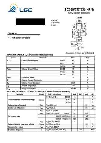
BC635/637/639(NPN) TO-92 Bipolar Transistors TO-92 1. EMITTER 2. COLLECTOR 3. BASE Features High current transistors Dimensions in inches and (millimeters) MAXIMUM RATINGS (TA=25 unless otherwise noted) Symbol Parameter Value Units VCBO Collector-Emitter Voltage BC635 45 V BC637 60 V BC639 100 V VCEO Collector-Emitter Voltage BC635 45 V BC637 60 V BC639 80 V ... See More ⇒
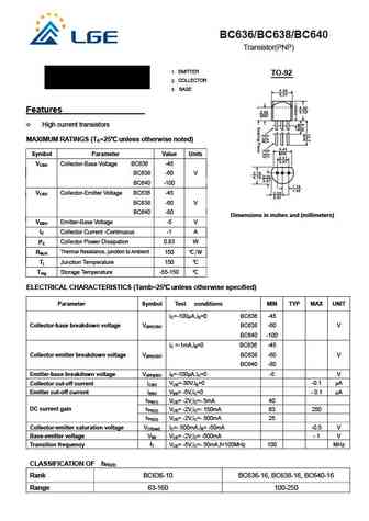
BC636/BC638/BC640 Transistor(PNP) 1. EMITTER TO-92 2. COLLECTOR 3. BASE Features High current transistors MAXIMUM RATINGS (TA=25 unless otherwise noted) Symbol Parameter Value Units VCBO Collector-Base Voltage BC636 -45 BC638 -60 V BC640 -100 VCEO Collector-Emitter Voltage BC636 -45 BC638 -60 V BC640 -80 Dimensions in inches and (millimeters) VEBO Emitter-... See More ⇒
AFC6332 Alfa-MOS 20V N & P Pair Technology Enhancement Mode MOSFET General Description Features AFC6332, N & P Pair enhancement mode N-Channel MOSFET, uses Advanced Trench Technology 20V/1.0A,RDS(ON)=280m @VGS=4.5V to provide excellent RDS(ON), low gate charge. 20V/0.8A,RDS(ON)=340m @VGS=2.5V These devices are particularly suited for low 20V/0.7A,RDS(ON)=580m @VGS=... See More ⇒
3CA638(BC638) PNP Ptot TC 75 1.5 W ICM 1.0 A Tjm 150 Tstg -55 150 V(BR)CBO ICB=0.1mA 60 V V(BR)CEO ICE=10mA 60 V V(BR)EBO IEB=10 A 5.0 V ICBO VCB=30V 0.1 A IEBO VEB=4V 0.1 A IC=0.5A VCEsat 0.5 V IB=0.05A VCE=2V hFE 63 25... See More ⇒
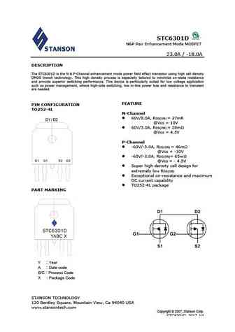
STC6301D N&P Pair Enhancement Mode MOSFET 23.0A / -18.0A DESCRIPTION The STC6301D is the N & P-Channel enhancement mode power field effect transistor using high cell density DMOS trench technology. This high density process is especially tailored to minimize on-state resistance and provide superior switching performance. This device is particularly suited for low voltage applicati... See More ⇒
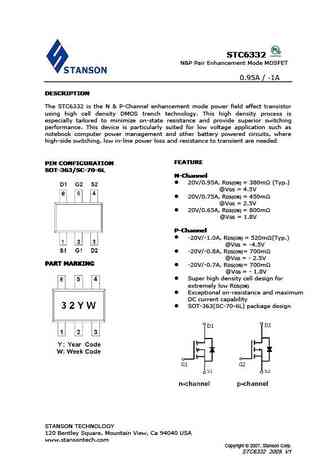
STC6332 STC6332 STC6332 STC6332 N&P Pair Enhancement Mode MOSFET 0.95A / -1A DESCRIPTION DESCRIPTION DESCRIPTION DESCRIPTION The STC6332 is the N & P-Channel enhancement mode power field effect transistor using high cell density DMOS trench technology. This high density process is especially tailored to minimize on-state resistance and provide superior switching performance. This d... See More ⇒
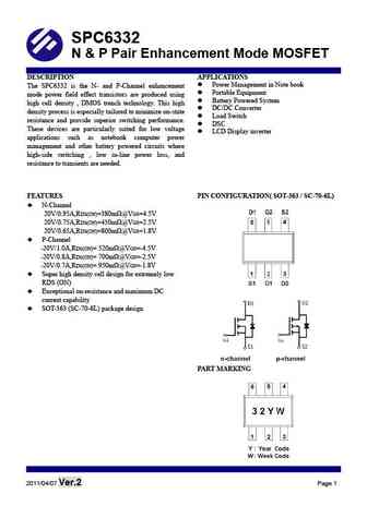
SPC6332 N & P Pair Enhancement Mode MOSFET DESCRIPTION APPLICATIONS Power Management in Note book The SPC6332 is the N- and P-Channel enhancement Portable Equipment mode power field effect transistors are produced using Battery Powered System high cell density , DMOS trench technology. This high DC/DC Converter density process is especially tailored to minimize on-sta... See More ⇒
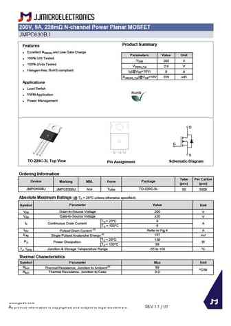
200V, 9A, 228m N-channel Power Planar MOSFET JMPC630BJ Product Summary Features Excellent RDS(ON) and Low Gate Charge Parameters Value Unit 100% UIS Tested VDSS 200 V 100% Vds Tested VGS(th)_Typ 2.9 V Halogen-free; RoHS-compliant ID(@VGS=10V) 9 A RDS(ON)_Typ(@VGS=10V 228 mW Applications Load Switch PWM Application Power Management D G S TO-2... See More ⇒
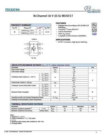
FDC637AN www.VBsemi.tw N-Channel 30 V (D-S) MOSFET FEATURES PRODUCT SUMMARY Halogen-free According to IEC 61249-2-21 Definition VDS (V) RDS(on) ( ) ID (A)a, e Qg (Typ.) TrenchFET Power MOSFET 0.030 at VGS = 10 V 6 Low On-Resistance 30 4.2 nC 0.040 at VGS = 4.5 V 6 100 % Rg Tested Compliant to RoHS Directive 2002/95/EC TSOP-6 APPLICATIONS DC/DC ... See More ⇒
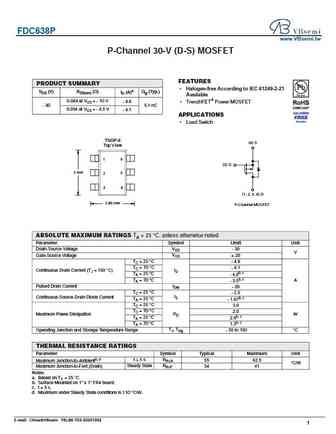
FDC638P www.VBsemi.tw P-Channel 30-V (D-S) MOSFET FEATURES PRODUCT SUMMARY Halogen-free According to IEC 61249-2-21 VDS (V) RDS(on) ( ) ID (A)a Qg (Typ.) Available 0.049 at VGS = - 10 V - 4.8 TrenchFET Power MOSFET - 30 5.1 nC 0.054 at VGS = - 4.5 V - 4.1 APPLICATIONS Load Switch TSOP-6 (4) S Top V iew 1 6 (3) G 3 mm 5 2 3 4 (1, 2, 5, 6) D 2.85 mm P-Cha... See More ⇒
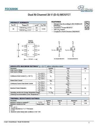
FDC6305N www.VBsemi.tw Dual N-Channel 20 V (D-S) MOSFET FEATURES PRODUCT SUMMARY Halogen-free According to IEC 61249-2-21 VDS (V) RDS(on) ( ) ID (A)a Qg (Typ.) Definition 0.022 at VGS = 4.5 V TrenchFET Power MOSFET 6.0 20 1.8 nC 100 % Rg Tested 0.028 at VGS = 2.5 V 5.0 Compliant to RoHS Directive 2002/95/EC TSOP-6 D1 D 2 D Top View G1 D1 1 6 G 1 ... See More ⇒
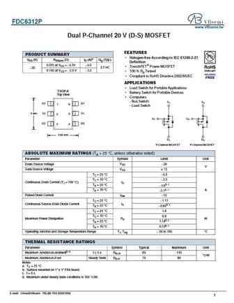
FDC6312P www.VBsemi.tw Dual P-Channel 20 V (D-S) MOSFET FEATURES PRODUCT SUMMARY Halogen-free According to IEC 61249-2-21 VDS (V) RDS(on) ( )ID (A)a Qg (Typ.) Definition 0.075 at VGS = - 4.5V - 4.0 TrenchFET Power MOSFET - 20 2.7 nC 0.100 at VGS = - 2.5 V - 3.2 100 % Rg Tested Compliant to RoHS Directive 2002/95/EC APPLICATIONS Load Switch for Portable Ap... See More ⇒
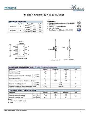
FDC6321C www.VBsemi.tw N- and P-Channel 2 V (D-S) MOSFET 0 FEATURES PRODUCT SUMMARY Halogen-free According to IEC 61249-2-21 VDS (V) RDS(on) ( )ID (A) Definition 0.024 at VGS = 10 V 5.5 TrenchFET Power MOSFET N-Channel 20 0.036 at VGS = 4.5 V 4.2 100 % Rg Tested 0.069 at VGS = - 10 V - 3.4 Compliant to RoHS Directive 2002/95/EC P-Channel - 20 0.083 at V... See More ⇒
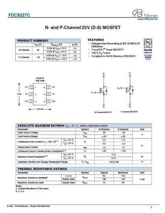
FDC6327C www.VBsemi.tw N- and P-Channel 2 V (D-S) MOSFET 0 FEATURES PRODUCT SUMMARY Halogen-free According to IEC 61249-2-21 VDS (V) RDS(on) ( )ID (A) Definition 0.024 at VGS = 10 V 5.5 TrenchFET Power MOSFET N-Channel 20 0.036 at VGS = 4.5 V 4.2 100 % Rg Tested 0.069 at VGS = - 10 V - 3.4 Compliant to RoHS Directive 2002/95/EC P-Channel - 20 0.083 at V... See More ⇒
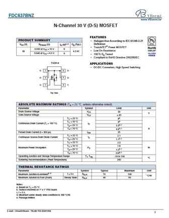
FDC637BNZ www.VBsemi.tw N-Channel 30 V (D-S) MOSFET FEATURES PRODUCT SUMMARY Halogen-free According to IEC 61249-2-21 Definition VDS (V) RDS(on) ( ) ID (A)a, e Qg (Typ.) TrenchFET Power MOSFET 0.030 at VGS = 10 V 6 Low On-Resistance 30 4.2 nC 0.040 at VGS = 4.5 V 6 100 % Rg Tested Compliant to RoHS Directive 2002/95/EC TSOP-6 APPLICATIONS DC/DC... See More ⇒
Detailed specifications: C5T5400, C5T5401, C5T5550, C5T5551, C5T6539, C5T6540, C5T918, C6, BC327, C64, C651, C652, C7, C7076, C720, C722, C740
Keywords - C63 pdf specs
C63 cross reference
C63 equivalent finder
C63 pdf lookup
C63 substitution
C63 replacement
