FT3906 Specs and Replacement
Type Designator: FT3906
Material of Transistor: Si
Polarity: PNP
Absolute Maximum Ratings
Maximum Collector Power Dissipation (Pc): 0.36 W
Maximum Collector-Base Voltage |Vcb|: 40 V
Maximum Collector-Emitter Voltage |Vce|: 40 V
Maximum Emitter-Base Voltage |Veb|: 5 V
Maximum Collector Current |Ic max|: 0.2 A
Max. Operating Junction Temperature (Tj): 175 °C
Electrical Characteristics
Transition Frequency (ft): 250 MHz
Collector Capacitance (Cc): 4.5 pF
Forward Current Transfer Ratio (hFE), MIN: 100
Package: TO18
FT3906 Substitution
- BJT ⓘ Cross-Reference Search
FT3906 datasheet
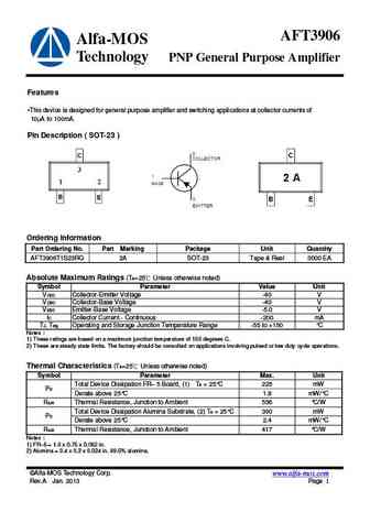
AFT3906 Alfa-MOS Technology PNP General Purpose Amplifier Features This device is designed for general purpose amplifier and switching applications at collector currents of 10 A to 100mA. Pin Description ( SOT-23 ) Ordering Information Part Ordering No. Part Marking Package Unit Quantity AFT3906T1S23RG 2A SOT-23 Tape & Reel 3000 EA Absolute Maximum Ratings (TA=25 Unless ... See More ⇒
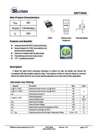
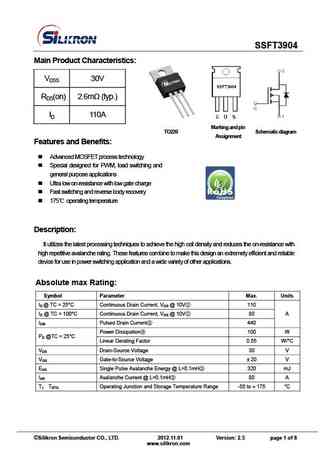
SSFT3906 Main Product Characteristics VDSS 30V SSFT3906 RDS(on) 3.2mohm(typ.) ID 90A TO220 Marking and pin Schematic diagram Assignment Features and Benefits Advanced trench MOSFET process technology Special designed for PWM, load switching and general purpose applications Ultra low on-resistance with low gate charge Fast switching and reverse body recove... See More ⇒
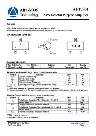
AFT3904 Alfa-MOS Technology NPN General Purpose Amplifier Features This device is designed as a general purpose amplifier and switch. The useful dynamic range extends to 100 mA as a switch and to 100 MHz as an amplifier. Pin Description ( SOT-23 ) Ordering Information Part Ordering No. Part Marking Package Unit Quantity AFT3904T1S23RG 1AM SOT-23 Tape & Reel 3000 EA A... See More ⇒
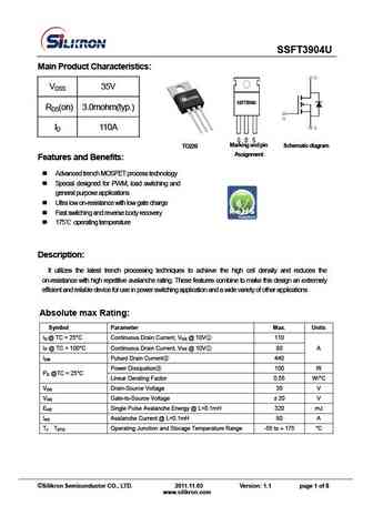
SSFT3904U Main Product Characteristics VDSS 35V SSFT3904U SSFT3904U RDS(on) 3.0mohm(typ.) ID 110A Ma r ki ng a n d pin Schema ti c di agr a m TO220 Assignment Features and Benefits Advanced trench MOSFET process technology Special designed for PWM, load switching and general purpose applications Ultra low on-resistance with low gate charge Fast sw... See More ⇒
Detailed specifications: FT359, FT3641, FT3642, FT3643, FT3644, FT3645, FT3722, FT3905, 2SC4793, FT40, FT400A, FT400B, FT401, FT4017, FT4018, FT4019, FT402
Keywords - FT3906 pdf specs
FT3906 cross reference
FT3906 equivalent finder
FT3906 pdf lookup
FT3906 substitution
FT3906 replacement
