2N4115 Datasheet. Specs and Replacement
Type Designator: 2N4115 📄📄
Material of Transistor: Si
Polarity: NPN
Absolute Maximum Ratings
Maximum Collector Power Dissipation (Pc): 37 W
Maximum Collector-Base Voltage |Vcb|: 120 V
Maximum Collector-Emitter Voltage |Vce|: 80 V
Maximum Emitter-Base Voltage |Veb|: 8 V
Maximum Collector Current |Ic max|: 5 A
Max. Operating Junction Temperature (Tj): 165 °C
Electrical Characteristics
Transition Frequency (ft): 50 MHz
Collector Capacitance (Cc): 120 pF
Forward Current Transfer Ratio (hFE), MIN: 40
Noise Figure, dB: -
Package: TO59
📄📄 Copy
- BJT ⓘ Cross-Reference Search
2N4115 datasheet
9.2. Size:68K vishay
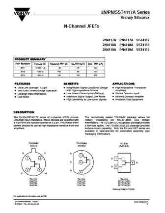
2n4117a pn4117a sst4117 2n4118a pn4118a sst4118 2n4119a pn4119a sst4119.pdf 

2N/PN/SST4117A Series Vishay Siliconix N-Channel JFETs 2N4117A PN4117A SST4117 2N4118A PN4118A SST4118 2N4119A PN4119A SST4119 PRODUCT SUMMARY Part Number VGS(off) (V) V(BR)GSS Min (V) gfs Min (mS) IDSS Min (mA) 4117 -0.6 to -1.8 -40 70 30 4118 -1 to -3 -40 80 80 4119 -2 to -6 -40 100 200 FEATURES BENEFITS APPLICATIONS D Ultra-Low Leakage 0.2 pA D Insignificant Signal Loss/Error Vo... See More ⇒
9.3. Size:12K semelab
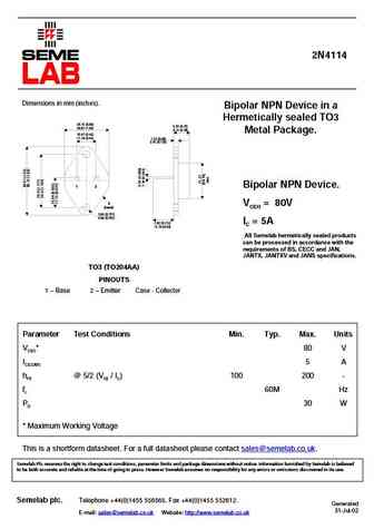
2n4114.pdf 

2N4114 Dimensions in mm (inches). Bipolar NPN Device in a Hermetically sealed TO3 25.15 (0.99) 6.35 (0.25) 26.67 (1.05) 9.15 (0.36) Metal Package. 10.67 (0.42) 11.18 (0.44) 1.52 (0.06) 3.43 (0.135) 1 2 Bipolar NPN Device. 3 VCEO = 80V (case) 3.84 (0.151) 4.09 (0.161) 7.92 (0.312) IC = 5A 12.70 (0.50) All Semelab hermetically sealed products can be processed in ac... See More ⇒
9.4. Size:11K semelab
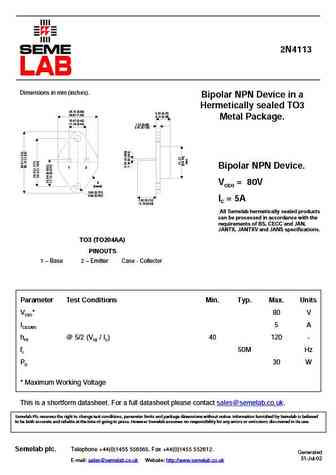
2n4113.pdf 

2N4113 Dimensions in mm (inches). Bipolar NPN Device in a Hermetically sealed TO3 25.15 (0.99) 6.35 (0.25) 26.67 (1.05) 9.15 (0.36) Metal Package. 10.67 (0.42) 11.18 (0.44) 1.52 (0.06) 3.43 (0.135) 1 2 Bipolar NPN Device. 3 VCEO = 80V (case) 3.84 (0.151) 4.09 (0.161) 7.92 (0.312) IC = 5A 12.70 (0.50) All Semelab hermetically sealed products can be processed in ac... See More ⇒
9.5. Size:21K calogic
2n4117 2n4118 2n4119 pn4117 pn4118 pn4119 sst4117 sst4118 sst4119.pdf 

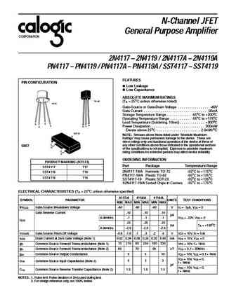
N-Channel JFET General Purpose Amplifier CORPORATION 2N4117 2N4119 / 2N4117A 2N4119A PN4117 PN4119 / PN4117A PN4119A / SST4117 SST4119 FEATURES PIN CONFIGURATION Low Leakage Low Capacitance ABSOLUTE MAXIMUM RATINGS TO-92 (T = 25oC unless otherwise noted) A TO-72 Gate-Source or Gate-Drain Voltage . . . . . . . . . . . . . . . . -40V Gate Curre... See More ⇒
9.6. Size:181K inchange semiconductor
2n4112.pdf 

isc Silicon NPN Power Transistor 2N4112 DESCRIPTION Excellent Safe Operating Area Low Collector-Emitter Saturation Voltage 100% avalanche tested Minimum Lot-to-Lot variations for robust device performance and reliable operation. APPLICATIONS Designed for general-purpose switching and amplifier applications ABSOLUTE MAXIMUM RATINGS(T =25 ) a SYMBOL PARAMETER VALUE UNIT V... See More ⇒
9.7. Size:181K inchange semiconductor
2n4114.pdf 

isc Silicon NPN Power Transistor 2N4114 DESCRIPTION Excellent Safe Operating Area Low Collector-Emitter Saturation Voltage 100% avalanche tested Minimum Lot-to-Lot variations for robust device performance and reliable operation. APPLICATIONS Designed for general-purpose switching and amplifier applications ABSOLUTE MAXIMUM RATINGS(T =25 ) a SYMBOL PARAMETER VALUE UNIT V... See More ⇒
9.8. Size:182K inchange semiconductor
2n4113.pdf 

isc Silicon NPN Power Transistor 2N4113 DESCRIPTION Excellent Safe Operating Area Low Collector-Emitter Saturation Voltage 100% avalanche tested Minimum Lot-to-Lot variations for robust device performance and reliable operation. APPLICATIONS Designed for general-purpose switching and amplifier applications ABSOLUTE MAXIMUM RATINGS(T =25 ) a SYMBOL PARAMETER VALUE UNIT V... See More ⇒
9.9. Size:181K inchange semiconductor
2n4111.pdf 
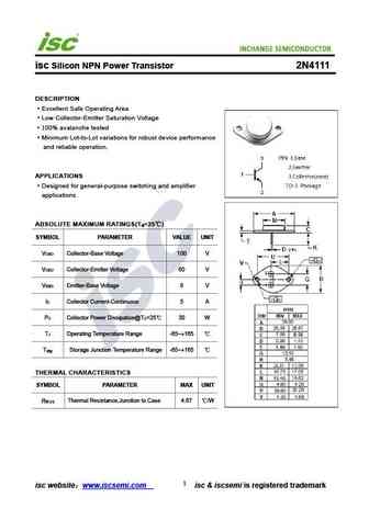
isc Silicon NPN Power Transistor 2N4111 DESCRIPTION Excellent Safe Operating Area Low Collector-Emitter Saturation Voltage 100% avalanche tested Minimum Lot-to-Lot variations for robust device performance and reliable operation. APPLICATIONS Designed for general-purpose switching and amplifier applications ABSOLUTE MAXIMUM RATINGS(T =25 ) a SYMBOL PARAMETER VALUE UNIT V... See More ⇒
Detailed specifications: 2N4105, 2N4106, 2N4106A, 2N411, 2N4111, 2N4112, 2N4113, 2N4114, BC327, 2N4116, 2N412, 2N4121, 2N4122, 2N4123, 2N4124, 2N4125, 2N4126
Keywords - 2N4115 pdf specs
2N4115 cross reference
2N4115 equivalent finder
2N4115 pdf lookup
2N4115 substitution
2N4115 replacement
![]()
