MA2 Specs and Replacement
Type Designator: MA2
Material of Transistor: Ge
Polarity: PNP
Absolute Maximum Ratings
Maximum Collector Power Dissipation (Pc): 0.02 W
Maximum Collector-Base Voltage |Vcb|: 30 V
Maximum Collector-Emitter Voltage |Vce|: 30 V
Maximum Collector Current |Ic max|: 0.05 A
Max. Operating Junction Temperature (Tj): 100 °C
Electrical Characteristics
Collector Capacitance (Cc): 6 pF
Forward Current Transfer Ratio (hFE), MIN: 245
Package: TO24
MA2 Substitution
- BJT ⓘ Cross-Reference Search
MA2 datasheet
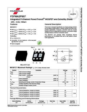
July 2014 FDFMA2P857 Integrated P-Channel PowerTrench MOSFET and Schottky Diode 20V, 3.0A, 120m Features General Description This device is designed specifically as a single package solution MOSFET for the battery charge switch in cellular handset and other ultra- Max rDS(on) = 120m at VGS = 4.5V, ID = 3.0A portable applications. It features a MOSFET with low on-s... See More ⇒
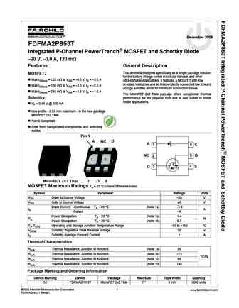
December 2008 FDFMA2P853T tm Integrated P-Channel PowerTrench MOSFET and Schottky Diode 20 V, 3.0 A, 120 m Features General Description This device is designed specifically as a single package solution MOSFET for the battery charge switch in cellular handset and other Max rDS(on) = 120 m at VGS = 4.5 V, ID = 3.0 A ultra-portable applications. It features a MOS... See More ⇒
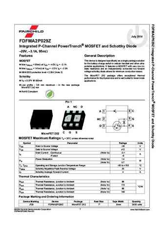
July 2014 FDFMA2P029Z Integrated P-Channel PowerTrench MOSFET and Schottky Diode 20V, 3.1A, 95m Features General Description MOSFET This device is designed specifically as a single package solution for the battery charge switch in cellular handset and other ultra- Max rDS(on) = 95m at VGS = 4.5V, ID = 3.1A portable applications. It features a MOSFET with very low on- ... See More ⇒
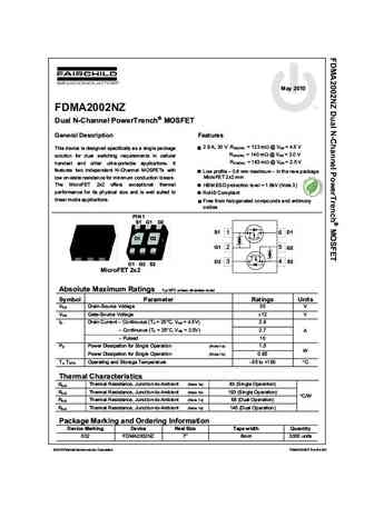
May 20 0 t tm tm tm FDMA2002NZ Dual N-Channel PowerTrench MOSFET General Description Features 2.9 A, 30 V RDS(ON) = 123 m @ VGS = 4.5 V This device is designed specifically as a single package RDS(ON) = 140 m @ VGS = 3.0 V solution for dual switching requirements in cellular RDS(ON) = 163 m @ VGS = 2.5 V handset and other ultra-portable applications. It fea... See More ⇒
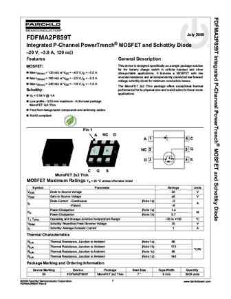
July 2009 FDFMA2P859T Integrated P-Channel PowerTrench MOSFET and Schottky Diode 20 V, 3.0 A, 120 m Features General Description This device is designed specifically as a single package solution MOSFET for the battery charge switch in cellular handset and other Max rDS(on) = 120 m at VGS = 4.5 V, ID = 3.0 A ultra-portable applications. It features a MOSFET with low... See More ⇒
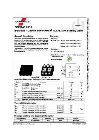
September 2008 July 2014 FDFMA2P853 Integrated P-Channel PowerTrench MOSFET and Schottky Diode General Description Features This device is designed specifically as a single package MOSFET solution for the battery charge switch in cellular handset -3.0 A, -20V. RDS(ON) = 120 m @ VGS = -4.5 V and other ultra-portable applications. It features a MOSFET with low on-state resis... See More ⇒
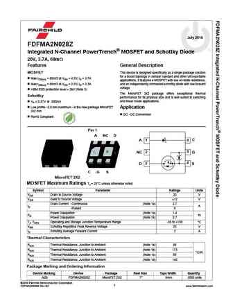
July 2014 FDFMA2N028Z Integrated N-Channel PowerTrench MOSFET and Schottky Diode 20V, 3.7A, 68m Features General Description MOSFET This device is designed specifically as a single package solution for a boost topology in cellular handset and other ultra-portable Max rDS(on) = 68m at VGS = 4.5V, ID = 3.7A applications. It features a MOSFET with low on-state resistance, Max ... See More ⇒
uma2n fma2a a2 sot23-5 sot353.pdf ![]()
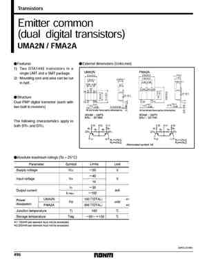
Transistors Emitter common (dual digital transistors) UMA2N / FMA2A FFeatures FExternal dimensions (Units mm) 1) Two DTA144E transistors in a single UMT and a SMT package. 2) Mounting cost and area can be cut in half. FStructure Dual PNP digital transistor (each with two built in resistors) The following characteristics apply to both DTr1 and DTr2. FAbsolute maximum ratings (Ta = ... See More ⇒
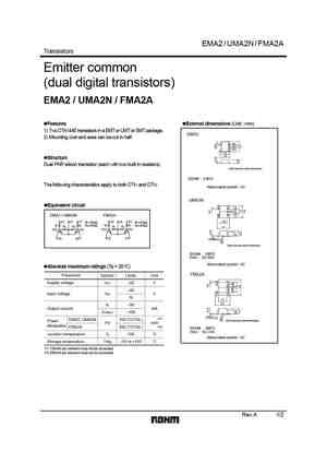
EMA2 / UMA2N / FMA2A Transistors Emitter common (dual digital transistors) EMA2 / UMA2N / FMA2A Features External dimensions (Unit mm) 1) Two DTA144E transistors in a EMT or UMT or SMT package. EMA2 2) Mounting cost and area can be cut in half. (4) (3) (2) (5) (1) 1.2 1.6 Structure Dual PNP silicon transistor (each with two built in resistors) Each lead has same ... See More ⇒
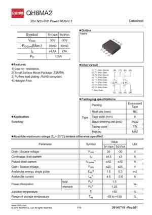
QH8MA2 Datasheet 30V Nch+Pch Power MOSFET lOutline l TSMT8 Symbol Tr1 Nch Tr2 Pch VDSS 30V -30V RDS(on)(Max.) 35m 80m ID 4.5A 3A PD 1.5W lFeatures l lInner circuit l 1) Low on - resistance. 2) Small Surface Mount Package (TSMT8). 3) Pb-free lead plati... See More ⇒
Is Now Part of To learn more about ON Semiconductor, please visit our website at www.onsemi.com Please note As part of the Fairchild Semiconductor integration, some of the Fairchild orderable part numbers will need to change in order to meet ON Semiconductor s system requirements. Since the ON Semiconductor product management systems do not have the ability to manage part nomenclatur... See More ⇒
This product complies with the RoHS Directive (EU 2002/95/EC). DMA26104 Silicon PNP epitaxial planar type For digital circuits Features Package Contributes to miniaturization of sets, reduction of component count. Code Eco-friendly Halogen-free package Mini5-G3-B Pin Name Basic Part Number 1 Base (Tr1) 4 Collector (Tr2) Dual DRA2114Y (Common emitter... See More ⇒
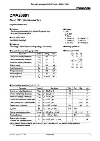
This product complies with the RoHS Directive (EU 2002/95/EC). DMA20601 Silicon PNP epitaxial planar type For general amplification Features Package Contributes to miniaturization of sets, reduction of component count. Code Eco-friendly Halogen-free package Mini6-G4-B Pin Name Basic Part Number 1 Emitter (Tr1) 4 Collector (Tr2) Dual DSA2001 (Individ... See More ⇒
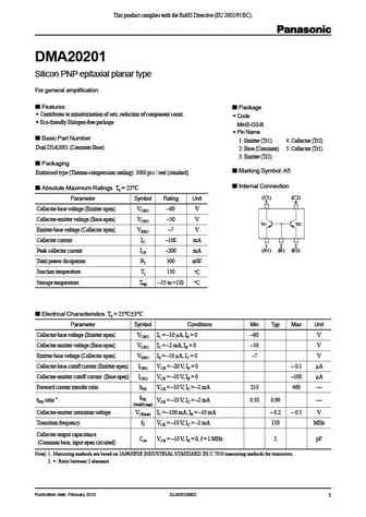
This product complies with the RoHS Directive (EU 2002/95/EC). DMA20201 Silicon PNP epitaxial planar type For general amplification Features Package Contributes to miniaturization of sets, reduction of component count. Code Eco-friendly Halogen-free package Mini5-G3-B Pin Name Basic Part Number 1 Emitter (Tr1) 4 Collector (Tr2) Dual DSA2001 (Common ... See More ⇒
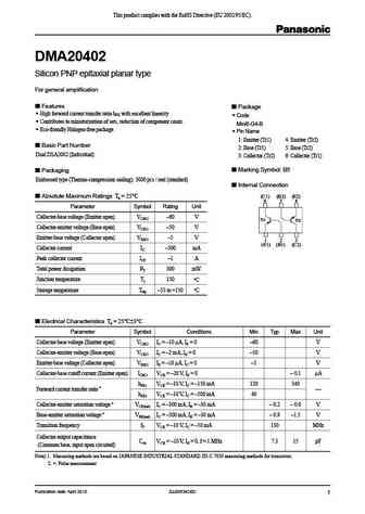
This product complies with the RoHS Directive (EU 2002/95/EC). DMA20402 Silicon PNP epitaxial planar type For general amplification Features Package High forward current transfer ratio hFE with excellent linearity Code Contributes to miniaturization of sets, reduction of component count. Mini6-G4-B Eco-friendly Halogen-free package Pin Name 1 Emitter (... See More ⇒
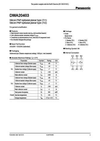
This product complies with the RoHS Directive (EU 2002/95/EC). DMA20403 Silicon PNP epitaxial planar type (Tr1) Silicon PNP epitaxial planar type (Tr2) For general amplification Features Package High forward current transfer ratio hFE with excellent linearity Code Low collector-emitter saturation voltage VCE(sat) Mini6-G4-B Contributes to miniaturization of s... See More ⇒
This product complies with the RoHS Directive (EU 2002/95/EC). DMA26406 Silicon PNP epitaxial planar type For digital circuits Features Package Contributes to miniaturization of sets, reduction of component count. Code Eco-friendly Halogen-free package Mini6-G4-B Pin Name Basic Part Number 1 Emitter (Tr1) 4 Emitter (Tr2) Dual DRA2143T (Individual) ... See More ⇒
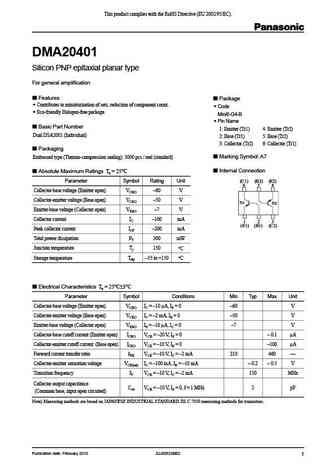
This product complies with the RoHS Directive (EU 2002/95/EC). DMA20401 Silicon PNP epitaxial planar type For general amplification Features Package Contributes to miniaturization of sets, reduction of component count. Code Eco-friendly Halogen-free package Mini6-G4-B Pin Name Basic Part Number 1 Emitter (Tr1) 4 Emitter (Tr2) Dual DSA2001 (Individual... See More ⇒
This product complies with the RoHS Directive (EU 2002/95/EC). DMA26102 Silicon PNP epitaxial planar type For digital circuits Features Package Contributes to miniaturization of sets, reduction of component count. Code Eco-friendly Halogen-free package Mini5-G3-B Pin Name Basic Part Number 1 Base (Tr1) 4 Collector (Tr2) Dual DRA2124E (Common emitter... See More ⇒
This product complies with the RoHS Directive (EU 2002/95/EC). DMA2610F Silicon PNP epitaxial planar type For digital circuits Features Package Contributes to miniaturization of sets, reduction of component count. Code Eco-friendly Halogen-free package Mini5-G3-B Pin Name Basic Part Number 1 Base (Tr1) 4 Collector (Tr2) Dual DRA2143X (Common emitter... See More ⇒
This product complies with the RoHS Directive (EU 2002/95/EC). DMA2610M Silicon PNP epitaxial planar type For digital circuits Features Package Contributes to miniaturization of sets, reduction of component count. Code Eco-friendly Halogen-free package Mini5-G3-B Pin Name Basic Part Number 1 Base (Tr1) 4 Collector (Tr2) Dual DRA2123J (Common emitter... See More ⇒
This product complies with the RoHS Directive (EU 2002/95/EC). DMA2610H Silicon PNP epitaxial planar type For digital circuits Features Package Contributes to miniaturization of sets, reduction of component count. Code Eco-friendly Halogen-free package Mini5-G3-B Pin Name Basic Part Number 1 Base (Tr1) 4 Collector (Tr2) Dual DRA2123Y (Common emitter... See More ⇒
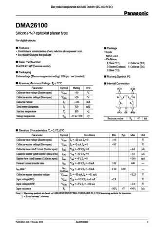
This product complies with the RoHS Directive (EU 2002/95/EC). DMA26100 Silicon PNP epitaxial planar type For digital circuits Features Package Contributes to miniaturization of sets, reduction of component count. Code Eco-friendly Halogen-free package Mini5-G3-B Pin Name Basic Part Number 1 Base (Tr1) 4 Collector (Tr2) Dual DRA2144T (Common emitter... See More ⇒
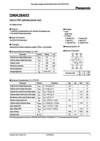
This product complies with the RoHS Directive (EU 2002/95/EC). DMA26403 Silicon PNP epitaxial planar type For digital circuits Features Package Contributes to miniaturization of sets, reduction of component count. Code Eco-friendly Halogen-free package Mini6-G4-B Pin Name Basic Part Number 1 Emitter (Tr1) 4 Emitter (Tr2) Dual DRA2144E (Individual) ... See More ⇒
This product complies with the RoHS Directive (EU 2002/95/EC). DMA26109 Silicon PNP epitaxial planar type For digital circuits Features Package Contributes to miniaturization of sets, reduction of component count. Code Eco-friendly Halogen-free package Mini5-G3-B Pin Name Basic Part Number 1 Base (Tr1) 4 Collector (Tr2) Dual DRA2113Z (Common emitter... See More ⇒
This product complies with the RoHS Directive (EU 2002/95/EC). DMA26401 Silicon PNP epitaxial planar type For digital circuits Features Package Contributes to miniaturization of sets, reduction of component count. Code Eco-friendly Halogen-free package Mini6-G4-B Pin Name Basic Part Number 1 Emitter (Tr1) 4 Emitter (Tr2) Dual DRA2114E (Individual) ... See More ⇒
This product complies with the RoHS Directive (EU 2002/95/EC). DMA26402 Silicon PNP epitaxial planar type For digital circuits Features Package Contributes to miniaturization of sets, reduction of component count. Code Eco-friendly Halogen-free package Mini6-G4-B Pin Name Basic Part Number 1 Emitter (Tr1) 4 Emitter (Tr2) Dual DRA2124E (Individual) ... See More ⇒
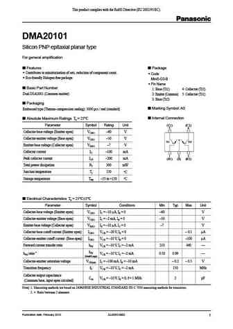
This product complies with the RoHS Directive (EU 2002/95/EC). DMA20101 Silicon PNP epitaxial planar type For general amplification Features Package Contributes to miniaturization of sets, reduction of component count. Code Eco-friendly Halogen-free package Mini5-G3-B Pin Name Basic Part Number 1 Base (Tr1) 4 Collector (Tr2) Dual DSA2001 (Common emit... See More ⇒
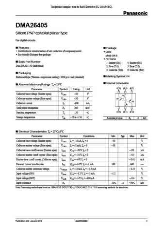
This product complies with the RoHS Directive (EU 2002/95/EC). DMA26405 Silicon PNP epitaxial planar type For digital circuits Features Package Contributes to miniaturization of sets, reduction of component count. Code Eco-friendly Halogen-free package Mini6-G4-B Pin Name Basic Part Number 1 Emitter (Tr1) 4 Emitter (Tr2) Dual DRA2114T (Individual) ... See More ⇒
This product complies with the RoHS Directive (EU 2002/95/EC). DMA26603 Silicon PNP epitaxial planar type For digital circuits Features Package Contributes to miniaturization of sets, reduction of component count. Code Eco-friendly Halogen-free package Mini6-G4-B Pin Name Basic Part Number 1 Emitter (Tr1) 4 Collector (Tr2) Dual DRA2144E (Individual)... See More ⇒
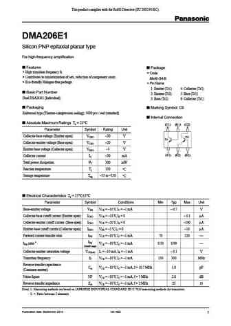
This product complies with the RoHS Directive (EU 2002/95/EC). DMA206E1 Silicon PNP epitaxial planar type For high-frequency amplification Features Package High transition frequency fT Code Contributes to miniaturization of sets, reduction of component count. Mini6-G4-B Eco-friendly Halogen-free package Pin Name 1 Emitter (Tr1) 4 Collector (Tr2) ... See More ⇒
This product complies with the RoHS Directive (EU 2002/95/EC). DMA26106 Silicon PNP epitaxial planar type For digital circuits Features Package Contributes to miniaturization of sets, reduction of component count. Code Eco-friendly Halogen-free package Mini5-G3-B Pin Name Basic Part Number 1 Base (Tr1) 4 Collector (Tr2) Dual DRA2143T (Common emitter... See More ⇒
This product complies with the RoHS Directive (EU 2002/95/EC). DMA26105 Silicon PNP epitaxial planar type For digital circuits Features Package Contributes to miniaturization of sets, reduction of component count. Code Eco-friendly Halogen-free package Mini5-G3-B Pin Name Basic Part Number 1 Base (Tr1) 4 Collector (Tr2) Dual DRA2114T (Common emitter... See More ⇒
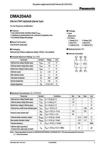
This product complies with the RoHS Directive (EU 2002/95/EC). DMA204A0 Silicon PNP epitaxial planar type For low frequency amplification Features Package Low collector-emitter saturation voltage VCE(sat) Code Contributes to miniaturization of sets, reduction of component count. Mini6-G4-B Eco-friendly Halogen-free package Pin Name 1 Emitter (Tr1) 4 E... See More ⇒
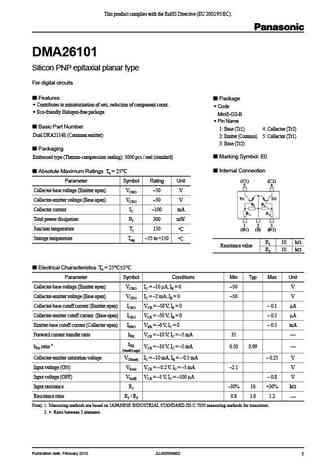
This product complies with the RoHS Directive (EU 2002/95/EC). DMA26101 Silicon PNP epitaxial planar type For digital circuits Features Package Contributes to miniaturization of sets, reduction of component count. Code Eco-friendly Halogen-free package Mini5-G3-B Pin Name Basic Part Number 1 Base (Tr1) 4 Collector (Tr2) Dual DRA2114E (Common emitter... See More ⇒
This product complies with the RoHS Directive (EU 2002/95/EC). DMA26103 Silicon PNP epitaxial planar type For digital circuits Features Package Contributes to miniaturization of sets, reduction of component count. Code Eco-friendly Halogen-free package Mini5-G3-B Pin Name Basic Part Number 1 Base (Tr1) 4 Collector (Tr2) Dual DRA2144E (Common emitter... See More ⇒
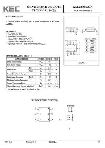
SEMICONDUCTOR KMA2D8P20X TECHNICAL DATA P-CH Trench MOSFET General Description It s mainly suitable for battery pack or power management in cell phone, and PDA. D H FEATURES J VDSS=-20V, ID=-2.8A. E Drain-Source ON Resistance. DIM MILLIMETERS RDS(ON)=90m (Max.) @ VGS=-4.5V A _ 3.00 0.15 A + F RDS(ON)=150m (Max.) @ VGS=-2.5V _ 1.65 0.1 + B _ + 2.85 0.2 C ... See More ⇒
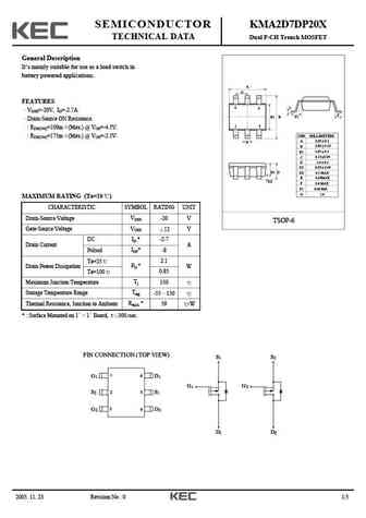
SEMICONDUCTOR KMA2D7DP20X TECHNICAL DATA Dual P-CH Trench MOSFET General Description It s mainly suitable for use as a load switch in battery powered applications. A G FEATURES 6 4 C VDSS=-20V, ID=-2.7A. F B1 B F1 Drain-Source ON Resistance. 1 3 RDS(ON)=100m (Max.) @ VGS=-4.5V. DIM MILLIMETERS RDS(ON)=175m (Max.) @ VGS=-2.5V. _ 3.05 + 0.1 A E _ 2.85 + 0.15 B _ 1... See More ⇒
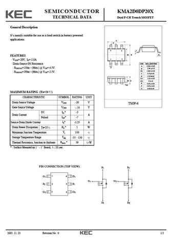
SEMICONDUCTOR KMA2D0DP20X TECHNICAL DATA Dual P-CH Trench MOSFET General Description It s mainly suitable for use as a load switch in battery powered applications. A F 6 4 C B1 B E FEATURES 1 3 VDSS=-20V, ID=-2.0A. DIM MILLIMETERS Drain-Source ON Resistance. _ 2.926 + 0.05 A G RDS(ON)=130m (Max.) @ VGS=-4.5V. _ B 2.80 + 0.15 _ B1 1.626 + 0.05 RDS(ON)=190m (Max.) @ ... See More ⇒
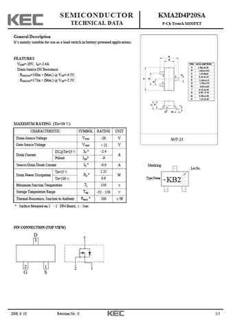
SEMICONDUCTOR KMA2D4P20SA TECHNICAL DATA P-Ch Trench MOSFET General Description It s mainly suitable for use as a load switch in battery powered applications. E FEATURES B VDSS=-20V, ID=-2.4A. DIM MILLIMETERS _ A 2.926 0.05 + Drain-Source ON Resistance. _ B 1.626 0.05 + C 1.25 MAX RDS(ON)=100m (Max.) @ VGS=-4.5V. 2 3 _ D 0.40 + 0.05 _ E 2.80 + 0.15 RDS(ON)=175m (M... See More ⇒
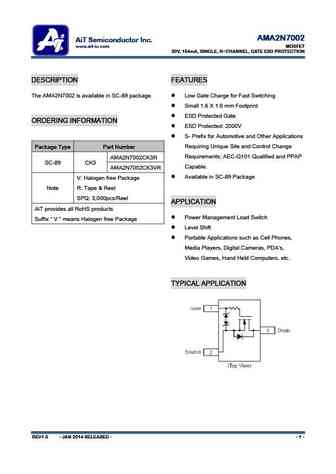
AMA2N7002 AiT Semiconductor Inc. www.ait-ic.com MOSFET 30V, 154mA, SINGLE, N-CHANNEL, GATE ESD PROTECTION DESCRIPTION FEATURES The AMA2N7002 is available in SC-89 package. Low Gate Charge for Fast Switching Small 1.6 X 1.6 mm Footprint ESD Protected Gate ORDERING INFORMATION ESD Protected 2000V S- Prefix for Automotive and Other Applications Requirin... See More ⇒
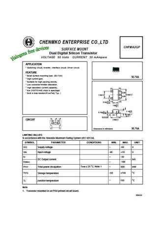
CHENMKO ENTERPRISE CO.,LTD CHFMA2GP SURFACE MOUNT Dual Digital Silicon Transistor VOLTAGE 50 Volts CURRENT 30 mAmpere APPLICATION * Switching circuit, Inverter, Interface circuit, Driver circuit. FEATURE * Small surface mounting type. (SC-74A) SC-74A * High current gain. * Suitable for high packing density. * Low colloector-emitter saturation. * High saturation current capability... See More ⇒
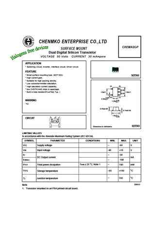
CHENMKO ENTERPRISE CO.,LTD CHEMA2GP SURFACE MOUNT Dual Digital Silicon Transistor VOLTAGE 50 Volts CURRENT 30 mAmpere APPLICATION * Switching circuit, Inverter, Interface circuit, Driver circuit. FEATURE * Small surface mounting type. (SOT-553) SOT553 * High current gain. * Suitable for high packing density. * Low colloector-emitter saturation. (4) (3) * High saturation current ... See More ⇒
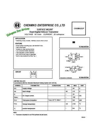
CHENMKO ENTERPRISE CO.,LTD CHUMA2GP SURFACE MOUNT Dual Digital Silicon Transistor VOLTAGE 50 Volts CURRENT 30 mAmpere APPLICATION * Switching circuit, Inverter, Interface circuit, Driver circuit. FEATURE * Small surface mounting type. (SC-88A/SOT-353) SC-88A/SOT353 * High current gain. * Suitable for high packing density. * Low colloector-emitter saturation. * High saturation cur... See More ⇒
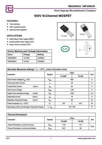
TMA20N65H, TMP20N65H Wuxi Unigroup Microelectronics Company 650V N-Channel MOSFET FEATURES Fast switching 100% avalanche tested Improved dv/dt capability APPLICATIONS Switch Mode Power Supply (SMPS) Uninterruptible Power Supply (UPS) Power Factor Correction (PFC) Device Marking and Package Information Device Package Marking TMA20N65H TO-220F A2... See More ⇒
tma2n60h tmd2n60h tmt2n60h tmu2n60h.pdf ![]()
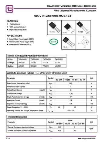
TMA2N60H,TMD2N60H,TMT2N60H,TMU2N60H Wuxi Unigroup Microelectronics Company Wuxi Unigroup Microelectronics Company 600V N-Channel MOSFET FEATURES Fast switching 100% avalanche tested Improved dv/dt capability APPLICATIONS Switch Mode Power Supply (SMPS) Uninterruptible Power Supply (UPS) Power Factor Correction (PFC) Device Marking and Package Info... See More ⇒
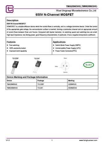
TMA20N65HG,TMW20N65HG Wuxi Unigroup Microelectronics Co.,Ltd 650V N-Channel MOSFET Description 650V N-Channel MOSFET VDMOSFET is a double-diffusion device which the current flows is vertically, and is a voltage-controlled device. Under the control of the appropriate gate voltage, the semiconductor surface is inverted, forming a conductive channel and an appropriate amount of curre... See More ⇒
Detailed specifications: MA117, MA1702, MA1703, MA1704, MA1705, MA1706, MA1707, MA1708, D667, MA200, MA201, MA202, MA203, MA204, MA2043, MA205, MA206
Keywords - MA2 pdf specs
MA2 cross reference
MA2 equivalent finder
MA2 pdf lookup
MA2 substitution
MA2 replacement
