MD6003 Datasheet. Specs and Replacement
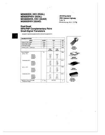
Type Designator: MD6003 📄📄
Material of Transistor: Si
Polarity: NPN*PNP
Absolute Maximum Ratings
Maximum Collector Power Dissipation (Pc): 0.4 W
Maximum Collector-Base Voltage |Vcb|: 50 V
Maximum Collector-Emitter Voltage |Vce|: 30 V
Maximum Emitter-Base Voltage |Veb|: 5 V
Maximum Collector Current |Ic max|: 0.5 A
Max. Operating Junction Temperature (Tj): 200 °C
Electrical Characteristics
Transition Frequency (ft): 170 MHz
Collector Capacitance (Cc): 5.6 pF
Forward Current Transfer Ratio (hFE), MIN: 100
Package: TO77
📄📄 Copy
MD6003 Substitution
- BJT ⓘ Cross-Reference Search
MD6003 datasheet
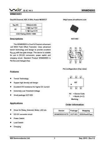
WNMD6003 WNMD6003 Dual N-Channel, 60V, 0.30A, Power MOSFET Http// www.sh-willsemi.com VDS (V) Rds(on) ( ) 1.4@ VGS=10V 60 1.7@ VGS=4.5V ESD Rating 2000V HBM SOT-563 Descriptions The WNMD6003 is Dual N-Channel enhancem -ent MOS Field Effect Transistor. Uses advanced D1 G2 S2 trench technology and design to provide excellent 6 5 4 RDS (ON) with low gate charge. This d... See More ⇒
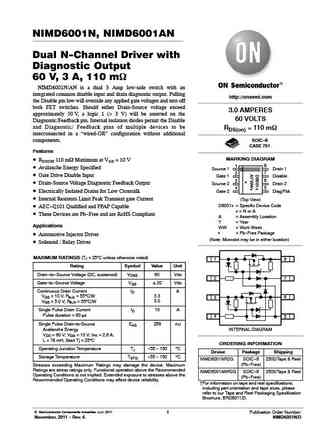
NIMD6001N, NIMD6001AN Dual N-Channel Driver with Diagnostic Output 60 V, 3 A, 110 mW NIMD6001N/AN is a dual 3 Amp low-side switch with an integrated common disable input and drain diagnostic output. Pulling http //onsemi.com the Disable pin low will override any applied gate voltages and turn off both FET switches. Should either Drain-Source voltage exceed 3.0 AMPERES approximately 50... See More ⇒
NIMD6001N, NIMD6001AN Dual N-Channel Driver with Diagnostic Output 60 V, 3 A, 110 mW NIMD6001N/AN is a dual 3 Amp low-side switch with an integrated common disable input and drain diagnostic output. Pulling http //onsemi.com the Disable pin low will override any applied gate voltages and turn off both FET switches. Should either Drain-Source voltage exceed 3.0 AMPERES approximately 50... See More ⇒
Detailed specifications: MD4260, MD4261, MD4957, MD5000, MD6001, MD6001F, MD6002, MD6002F, S9014, MD6003F, MD6100, MD6100F, MD6900, MD696, MD696A, MD698, MD698A
Keywords - MD6003 pdf specs
MD6003 cross reference
MD6003 equivalent finder
MD6003 pdf lookup
MD6003 substitution
MD6003 replacement


