MN25 Datasheet. Specs and Replacement
Type Designator: MN25 📄📄
Material of Transistor: Ge
Polarity: PNP
Absolute Maximum Ratings
Maximum Collector Power Dissipation (Pc): 45 W
Maximum Collector-Base Voltage |Vcb|: 40 V
Maximum Collector Current |Ic max|: 3 A
Max. Operating Junction Temperature (Tj): 85 °C
Electrical Characteristics
Transition Frequency (ft): 0.3 MHz
Forward Current Transfer Ratio (hFE), MIN: 25
Noise Figure, dB: -
Package: TO3
📄📄 Copy
- BJT ⓘ Cross-Reference Search
MN25 datasheet
0.1. Size:260K nxp
pmn25ene.pdf 
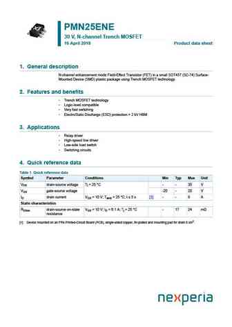
PMN25ENE 30 V, N-channel Trench MOSFET 16 April 2018 Product data sheet 1. General description N-channel enhancement mode Field-Effect Transistor (FET) in a small SOT457 (SC-74) Surface- Mounted Device (SMD) plastic package using Trench MOSFET technology. 2. Features and benefits Trench MOSFET technology Logic-level compatible Very fast switching ElectroStatic Discharg... See More ⇒
0.2. Size:260K nxp
pmn25enea.pdf
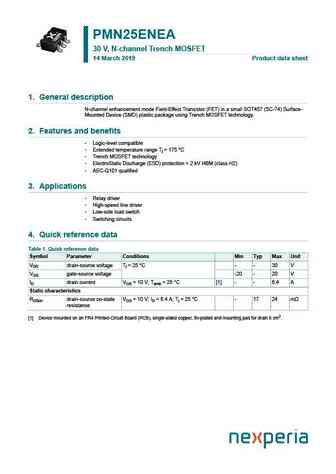
PMN25ENEA 30 V, N-channel Trench MOSFET 14 March 2019 Product data sheet 1. General description N-channel enhancement mode Field-Effect Transistor (FET) in a small SOT457 (SC-74) Surface- Mounted Device (SMD) plastic package using Trench MOSFET technology. 2. Features and benefits Logic-level compatible Extended temperature range Tj = 175 C Trench MOSFET technology E... See More ⇒
0.3. Size:278K diodes
dmn2550ufa.pdf
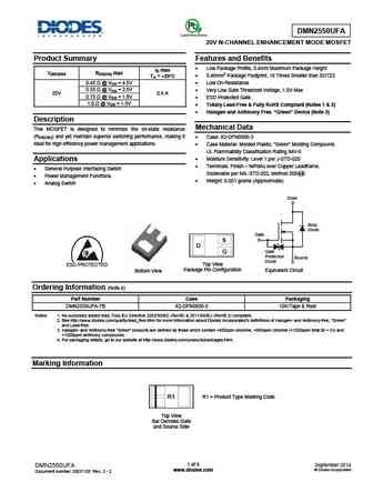
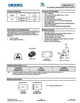
DMN2550UFA 20V N-CHANNEL ENHANCEMENT MODE MOSFET Product Summary Features and Benefits Low Package Profile, 0.4mm Maximum Package Height ID max V(BR)DSS RDS(ON) max 0.48mm2 Package Footprint, 16 Times Smaller than SOT23 TA = +25 C 0.45 @ VGS = 4.5V Low On-Resistance 0.55 @ VGS = 2.5V Very Low Gate Threshold Voltage, 1.0V Max 20V 0.6 A 0.75 @ VG... See More ⇒
0.4. Size:570K diodes
dmn2501ufb4.pdf
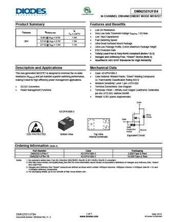
DMN2501UFB4 N-CHANNEL ENHANCEMENT MODE MOSFET Product Summary Features and Benefits Low On-Resistance ID V(BR)DSS RDS(on) max Very Low Gate Threshold Voltage VGS(TH), 1.0V Max. TA = +25 C Low Input Capacitance 0.4 @ VGS = 4.5V 1.5A Fast Switching Speed 20V 0.5 @ VGS = 2.5V 1.3A Ultra-Small Surfaced Mount Package 0.7 @ VGS = 1.8V 1.1A ... See More ⇒
0.5. Size:124K diodes
dmn2500ufb4.pdf
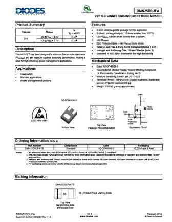
DMN2500UFB4 N-CHANNEL ENHANCEMENT MODE MOSFET Product Summary Features and Benefits Low On-Resistance ID V(BR)DSS RDS(on) max Very Low Gate Threshold Voltage VGS(TH), 1.0V max TA = 25 C Low Input Capacitance Fast Switching Speed 0.4 @ VGS = 4.5V 1A 20V Ultra-Small Surfaced Mount Package 0.7 @ VGS = 1.8V 0.8A Ultra-low package profile, 0.4mm max... See More ⇒
0.6. Size:279K diodes
dmn25d0ufa.pdf
DMN25D0UFA 25V N-CHANNEL ENHANCEMENT MODE MOSFET Product Summary Features ID 0.4mm ultra low profile package for thin application V(BR)DSS RDS(on) TA = +25 C 0.48mm2 package footprint, 16 times smaller than SOT23 Low VGS(th), can be driven directly from a battery 4 @ VGS = 4.5V 0.32A 25V Low RDS(on) 5 @ VGS = 2.7V 0.28A ESD Protected Gate (>6kV Hu... See More ⇒
0.7. Size:68K utc
mn2510.pdf
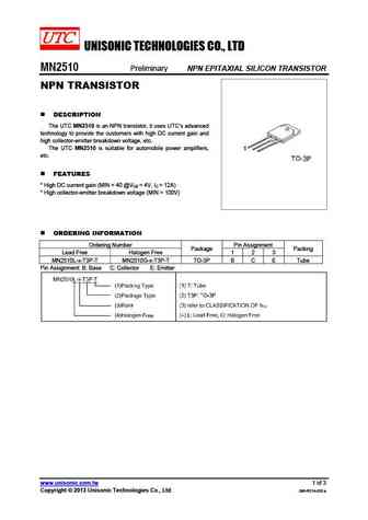
UNISONIC TECHNOLOGIES CO., LTD MN2510 Preliminary NPN EPITAXIAL SILICON TRANSISTOR NPN TRANSISTOR DESCRIPTION The UTC MN2510 is an NPN transistor, it uses UTC s advanced technology to provide the customers with high DC current gain and high collector-emitter breakdown voltage, etc. The UTC MN2510 is suitable for automobile power amplifiers, etc. FEATURES * High DC ... See More ⇒
0.8. Size:633K auk
sjmn250r80zw.pdf
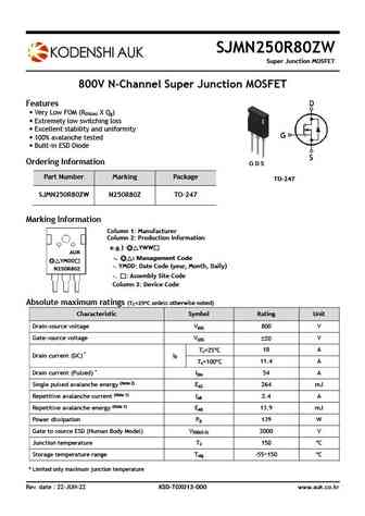
SJMN250R80ZW Super Junction MOSFET 800V N-Channel Super Junction MOSFET Features Very Low FOM (R X Q ) DS(on) g Extremely low switching loss Excellent stability and uniformity 100% avalanche tested Built-in ESD Diode Ordering Information G D S Part Number Marking Package TO-247 SJMN250R80ZW N250R80Z TO-247 Marking Information Column 1 Manufac... See More ⇒
0.9. Size:657K auk
sjmn250r80zf.pdf
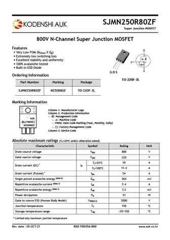
SJMN250R80ZF Super Junction MOSFET 800V N-Channel Super Junction MOSFET Features Very Low FOM (R X Q ) DS(on) g Extremely low switching loss Excellent stability and uniformity 100% avalanche tested Built-in ESD Diode G D S Ordering Information TO-220F-3L Part Number Marking Package SJMN250R80ZF N250R80Z TO-220F-3L Marking Information Column 1 ... See More ⇒
0.10. Size:630K auk
sjmn250r80zb.pdf
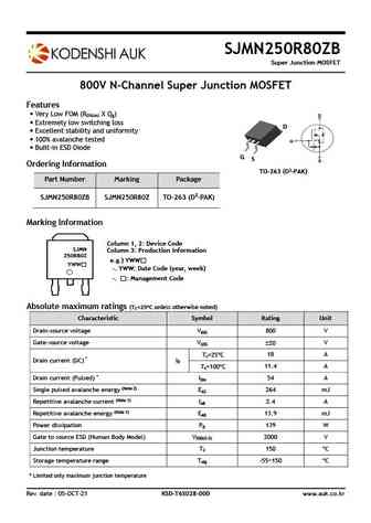
SJMN250R80ZB Super Junction MOSFET 800V N-Channel Super Junction MOSFET Features Very Low FOM (R X Q ) DS(on) g Extremely low switching loss D Excellent stability and uniformity 100% avalanche tested Built-in ESD Diode G S Ordering Information TO-263 (D2-PAK) Part Number Marking Package SJMN250R80ZB SJMN250R80Z TO-263 (D2-PAK) Marking Inform... See More ⇒
0.11. Size:653K auk
sjmn250r80zp.pdf

SJMN250R80ZP Super Junction MOSFET 800V N-Channel Super Junction MOSFET Features Very Low FOM (R X Q ) DS(on) g Extremely low switching loss Excellent stability and uniformity 100% avalanche tested Built-in ESD Diode G D S Ordering Information TO-220AB-3L Part Number Marking Package SJMN250R80ZP N250R80Z TO-220AB-3L Marking Information Column ... See More ⇒
0.12. Size:142K m-mos
mmn25n03.pdf
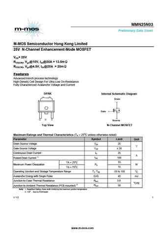
MMN25N03 Preliminary Data Sheet M-MOS Semiconductor Hong Kong Limited 25V N-Channel Enhancement-Mode MOSFET VDS= 25V RDS(ON), Vgs@10V, Ids@20A = 13.5m RDS(ON), Vgs@4.5V, Ids@20A = 20m Features Advanced trench process technology High Density Cell Design For Ultra Low On-Resistance Fully Characterized Avalanche Voltage and Current DPAK Internal Schematic Diagram Drain Gate S... See More ⇒
0.13. Size:677K way-on
wml25n50c4 wmo25n50c4 wmk25n50c4 wmn25n50c4 wmm25n50c4 wmj25n50c4.pdf
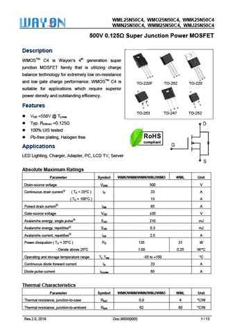
WML25N50C4, WMO25N5 WM C4 W 50C4, MK25N50C WMN2 MJ25N50C 25N50C4, WMM25N50C4, WM C4 500V 0.125 S 0 Super Junction Power MOSFET Descrip ption WMOSTM C4 is Wa 4th generation super ayon s n junction MOSFET fa that is utilizing charge M amily S balance te or extremely esistance echnology fo y low on-re S D D G G G S D G and low ga charge performanc WMOSTM ... See More ⇒
0.14. Size:650K way-on
wml25n65em wmk25n65em wmn25n65em wmm25n65em wmj25n65em.pdf

WML25N6 MK25N65EM W 65EM, WM WMN25 WMM25N6 MJ25N65EM 5N65EM, W 65EM, WM 650V 0.165 S 0 Super Junction Power MOSFET Descrip ption WMOSTM EM is Wayon s 3rd generation super W n junction MOSFET fa that is utilizing charge M amily S balance te or extremely esistance echnology fo y low on-re S D D G G G S D G T and low ga ce. WMOSTM EM is ate charge perf... See More ⇒
0.15. Size:668K way-on
wml25n80m3 wmm25n80m3 wmn25n80m3 wmj25n80m3 wmk25n80m3.pdf
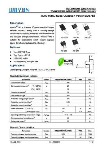
WML25N8 MM25N80M 80M3, WM M3 WMN2 80M3, WM M3 25N80M3, WMJ25N8 MK25N80M 800V 0.21 S T V Super Junction Power MOSFET Descrip ption WMOSTM M3 is Wayo neration 800 M on s 3rd gen 0V super junction MOSFET fa that is utilizing charge M amily S balance te or extremely esistance echnology fo y low on-re S D D G G G S D G T and low ga charge performanc WMOSTM ... See More ⇒
0.16. Size:655K way-on
wml25n70em wmk25n70em wmn25n70em wmm25n70em wmj25n70em.pdf

WML25N7 MK25N70EM W 70EM, WM WMN25 WMM25N7 MJ25N70EM 5N70EM, W 70EM, WM 700V 0.165 S 0 Super Junction Power MOSFET Descrip ption WMOSTM EM is Wayon s 3rd generation super W n junction MOSFET fa that is utilizing charge M amily S balance te or extremely esistance echnology fo y low on-re S D D G G G S D G T and low ga ce. WMOSTM EM is ate charge perf... See More ⇒
Detailed specifications: MMUN2134LT1, MMUN2134LT2, MN13A, MN13B, MN13C, MN19, MN21, MN24, 2SC4793, MN26, MN28, MN29, MN32, MN48, MN49, MO810, MO816
Keywords - MN25 pdf specs
MN25 cross reference
MN25 equivalent finder
MN25 pdf lookup
MN25 substitution
MN25 replacement
