P303 Datasheet. Specs and Replacement
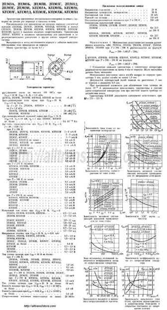
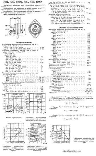
Type Designator: P303 📄📄
Material of Transistor: Si
Polarity: PNP
Absolute Maximum Ratings
Maximum Collector Power Dissipation (Pc): 5 W
Maximum Collector-Base Voltage |Vcb|: 60 V
Maximum Collector Current |Ic max|: 0.5 A
Max. Operating Junction Temperature (Tj): 150 °C
Electrical Characteristics
Transition Frequency (ft): 0.1 MHz
Forward Current Transfer Ratio (hFE), MIN: 6
Noise Figure, dB: -
- BJT ⓘ Cross-Reference Search
P303 datasheet
0.1. Size:121K motorola
tp3034re.pdf 

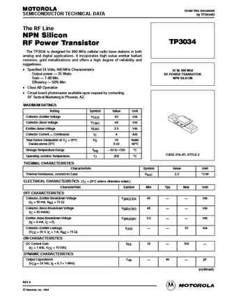
MOTOROLA Order this document SEMICONDUCTOR TECHNICAL DATA by TP3034/D The RF Line NPN Silicon TP3034 RF Power Transistor The TP3034 is designed for 960 MHz cellular radio base stations in both analog and digital applications. It incoporates high value emitter ballast resistors, gold metallizations and offers a high degree of reliability and ruggedness. Specified 24 Volts, 960 MH... See More ⇒
0.2. Size:117K motorola
tp3032re.pdf 

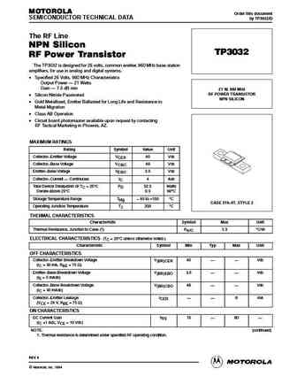
MOTOROLA Order this document SEMICONDUCTOR TECHNICAL DATA by TP3032/D The RF Line NPN Silicon TP3032 RF Power Transistor The TP3032 is designed for 26 volts, common emitter, 960 MHz base station amplifiers, for use in analog and digital systems. Specified 26 Volts, 960 MHz Characteristics Output Power 21 Watts Gain 7.5 dB min 21 W, 960 MHz RF POWER TRANSISTOR Sili... See More ⇒
0.3. Size:305K international rectifier
irlp3034pbf.pdf 

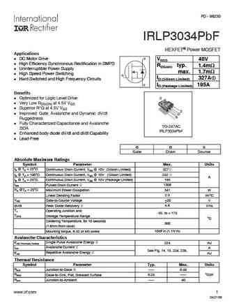
PD - 96230 IRLP3034PbF HEXFET Power MOSFET Applications D l DC Motor Drive VDSS 40V l High Efficiency Synchronous Rectification in SMPS RDS(on) typ. 1.4m l Uninterruptible Power Supply max. 1.7m l High Speed Power Switching G ID (Silicon Limited) 327A l Hard Switched and High Frequency Circuits S ID (Package Limited) 195A Benefits l Optimized for Logic Level Drive D ... See More ⇒
0.4. Size:53K sanyo
fp303.pdf 

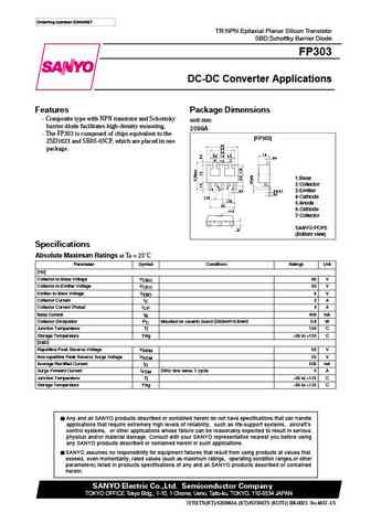
Ordering number ENN4657 TR NPN Epitaxial Planar Silicon Transistor SBD Schottky Barrier Diode FP303 DC-DC Converter Applications Features Package Dimensions Composite type with NPN transistor and Schottoky unit mm barrier diode facilitates high-density mounting. 2099A The FP303 is composed of chips equivalent to the [FP303] 2SD1623 and SB05-05CP, which are placed in one 4.5... See More ⇒
0.5. Size:25K siemens
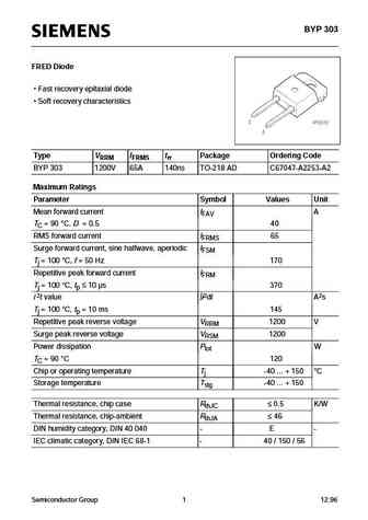
byp303.pdf 

BYP 303 FRED Diode Fast recovery epitaxial diode Soft recovery characteristics Type VRRM IFRMS trr Package Ordering Code BYP 303 1200V 65A 140ns TO-218 AD C67047-A2253-A2 Maximum Ratings Parameter Symbol Values Unit Mean forward current IFAV A TC = 90 C, D = 0.5 40 RMS forward current IFRMS 65 Surge forward current, sine halfwave, aperiodic IFSM Tj = 100 C, f = 50 Hz 170... See More ⇒
0.6. Size:431K siemens
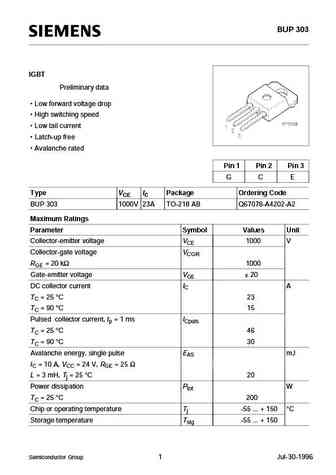
bup303.pdf 

BUP 303 IGBT Preliminary data Low forward voltage drop High switching speed Low tail current Latch-up free Avalanche rated Pin 1 Pin 2 Pin 3 G C E Type VCE IC Package Ordering Code BUP 303 1000V 23A TO-218 AB Q67078-A4202-A2 Maximum Ratings Parameter Symbol Values Unit Collector-emitter voltage VCE 1000 V Collector-gate voltage VCGR RGE = 20 k 1000 Gate-... See More ⇒
0.7. Size:305K diodes
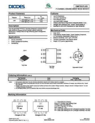
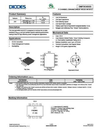
dmp3037lss.pdf 

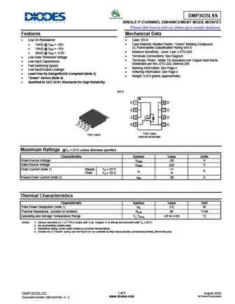
DMP3037LSS P-CHANNEL ENHANCEMENT MODE MOSFET Product Summary Features Low On-Resistance ID V(BR)DSS RDS(on) max Low Input Capacitance TC = +25 C Fast Switching Speed 32m @ VGS = -10V -5.8A -30V Low Input/Output Leakage 50m @ VGS = -4.5V -4.6A Totally Lead-Free & Fully RoHS Compliant (Notes 1 & 2) Halogen and Antimony Free. Green Devi... See More ⇒
0.8. Size:268K diodes
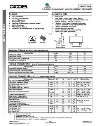
dmp3030sn.pdf 

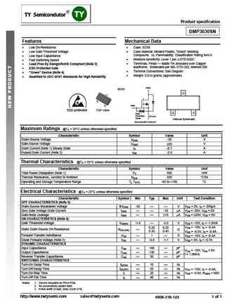
DMP3030SN P-CHANNEL ENHANCEMENT MODE FIELD EFFECT TRANSISTOR Features Mechanical Data Low On-Resistance Case SC-59 Low Gate Threshold Voltage Case Material Molded Plastic, Green Molding Compound. UL Flammability Classification Rating 94V-0 Low Input Capacitance Moisture sensitivity Level 1 per J-STD-020C Fast Switching Speed Lead Free By... See More ⇒
0.9. Size:382K diodes
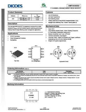
dmp3036ssd.pdf 

DMP3036SSD P-CHANNEL ENHANCEMENT MODE MOSFET Product Summary Features ID Low On-Resistance V(BR)DSS RDS(on) max TC = +25 C Low Input Capacitance 20m @ VGS = -10V -18.0A -30V Fast Switching Speed -15.0A 29m @ VGS = -5V Totally Lead-Free & Fully RoHS Compliant (Notes 1 & 2) Halogen and Antimony Free. Green Device (Note 3) Description ... See More ⇒
0.10. Size:194K diodes
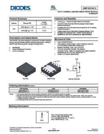
dmp3035sfg.pdf 

DMP3035SFG 30V P-CHANNEL ENHANCEMENT MODE MOSFET POWERDI Product Summary Features and Benefits Low RDS(ON) ensures on state losses are minimized ID max V(BR)DSS RDS(ON) max Small form factor thermally efficient package enables higher TA = 25 C density end products 20m @ VGS = -10V -9.5 A Occupies just 33% of the board area occupied by SO-8 enabling -... See More ⇒
0.12. Size:420K diodes
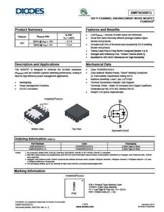
dmp3036sfg.pdf 

DMP3036SFG 30V P-CHANNEL ENHANCEMENT MODE MOSFET POWERDI Product Summary Features and Benefits ID max Low RDS(ON) ensures on state losses are minimized. V(BR)DSS RDS(ON) max TA = +25 C Small form factor thermally efficient package enables higher density end products. 20m @ VGS = -10V - 8.7 A -30V Occupies just 33% of the board area occupied by SO-8 enab... See More ⇒
0.14. Size:537K diodes
dmp3036sfv.pdf 

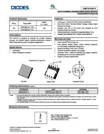
DMP3036SFV 30V P-CHANNEL ENHANCEMENT MODE MOSFET PowerDI3333-8 (Type UX) Product Summary Features Low RDS(ON) Ensures On State Losses Are Minimized ID Max BVDSS RDS(ON) Max Small Form Factor Thermally Efficient Package Enables Higher TC = +25 C Density End Products 20m @ VGS = -10V Occupies Just 33% of The Board Area Occupied by SO-8 -30V -30A 29m... See More ⇒
0.15. Size:202K onsemi
ntmsd3p303r2-d.pdf 

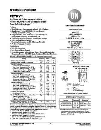
NTMSD3P303R2 FETKY P-Channel Enhancement-Mode Power MOSFET and Schottky Diode Dual SO-8 Package Features High Efficiency Components in a Single SO-8 Package http //onsemi.com High Density Power MOSFET with Low RDS(on), MOSFET Schottky Diode with Low VF -3.05 AMPERES Independent Pin-Outs for MOSFET and Schottky Die -30 VOLTS Allowing for Flexibility in Application Use... See More ⇒
0.18. Size:57K tysemi
dmp3030sn.pdf 

Product specification DMP3030SN Features Mechanical Data Low On-Resistance Case SC59 Low Gate Threshold Voltage Case Material Molded Plastic, Green Molding Compound. UL Flammability Classification Rating 94V-0 Low Input Capacitance Moisture sensitivity Level 1 per J-STD-020C Fast Switching Speed Terminals Finish Matte Tin annealed ove... See More ⇒
0.19. Size:361K cn vbsemi
vbc6p3033.pdf 

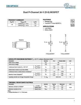
VBC6P3033 www.VBsemi.com Dual P-Channel 30-V (D-S) MOSFET FEATURES PRODUCT SUMMARY Halogen-free VDS (V) RDS(on) ( )ID (A) TrenchFET Power MOSFETs 0.036 at VGS = - 10 V - 5.2 - 30 RoHS 0.055 at VGS = - 4.5 V - 4.2 COMPLIANT APPLICATIONS Load Switch Battery Switch S1 S2 TSSOP-8 G1 G2 D1 1 D2 8 S1 2 S2 7 S1 3 S2 6 G1 4 G2 5 Top View D1 D2 ... See More ⇒
0.20. Size:243K inchange semiconductor
irlp3034.pdf 
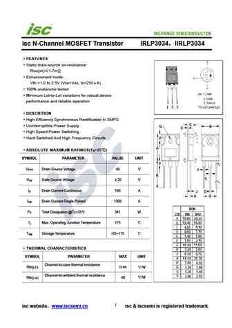
INCHANGE Semiconductor isc N-Channel MOSFET Transistor IRLP3034 IIRLP3034 FEATURES Static drain-source on-resistance RDS(on) 1.7m Enhancement mode Vth =1.0 to 2.5V (VDS=VGS, ID=250 A) 100% avalanche tested Minimum Lot-to-Lot variations for robust device performance and reliable operation DESCRITION High Efficiency Synchronous Rectification in SMPS Uninterru... See More ⇒
Detailed specifications: P217V, P27, P27A, P28, P29, P29A, P30, P302, S9018, P303A, P304, P306, P306A, P307, P307A, P307B, P307G
Keywords - P303 pdf specs
P303 cross reference
P303 equivalent finder
P303 pdf lookup
P303 substitution
P303 replacement
