SE1001 Specs and Replacement
Type Designator: SE1001
Material of Transistor: Si
Polarity: NPN
Absolute Maximum Ratings
Maximum Collector Power Dissipation (Pc): 0.2 W
Maximum Collector-Base Voltage |Vcb|: 45 V
Maximum Collector-Emitter Voltage |Vce|: 45 V
Maximum Emitter-Base Voltage |Veb|: 4 V
Maximum Collector Current |Ic max|: 0.1 A
Max. Operating Junction Temperature (Tj): 125 °C
Electrical Characteristics
Transition Frequency (ft): 200 MHz
Collector Capacitance (Cc): 4 pF
Forward Current Transfer Ratio (hFE), MIN: 40
Package: TO106
SE1001 Substitution
- BJT ⓘ Cross-Reference Search
SE1001 datasheet
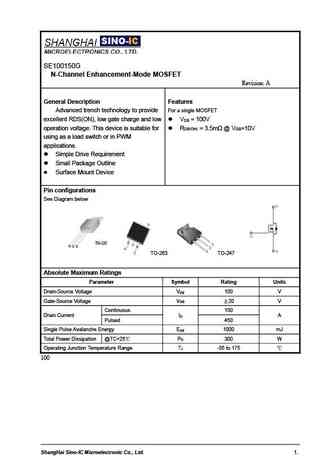
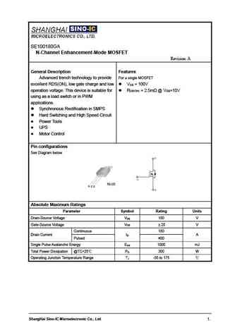
SE100150G N-Channel Enhancement-Mode MOSFET Revision A General Description Features For a single MOSFET Advanced trench technology to provide excellent RDS(ON), low gate charge and low V =100V DS operation voltage. This device is suitable for R =3.5m @V =10V DS(ON) GS using as a load switch or in PWM applications. Simple Drive Requirement Small Package Outline ... See More ⇒
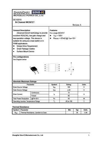
SE10015 N-Channel MOSFET Revision A General Description Features For a single MOSFET Advanced trench technology to provide excellent RDS(ON), low gate charge and V =100V DS low operation voltage. This device is R =67m @V =10V DS(ON) GS suitable for using as a load switch or in PWM applications. Simple Drive Requirement Small Package Outline Surface Mount De... See More ⇒
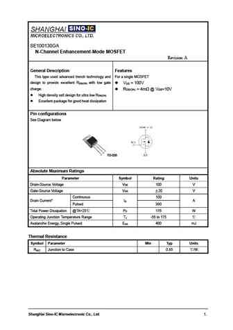
SE100130GA N-Channel Enhancement-Mode MOSFET Revision A General Description Features This type used advanced trench technology and For a single MOSFET design to provide excellent R with low gate DS(ON) V =100V DS charge. R =4m @V =10V DS(ON) GS High density cell design for ultra low R DS(ON) Excellent package for good heat dissipation Pin configurations See Di... See More ⇒
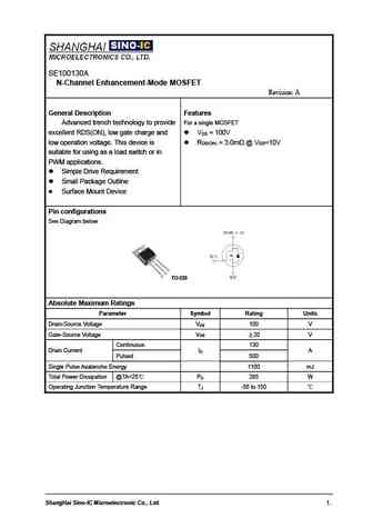
SE100130A N-Channel Enhancement-Mode MOSFET Revision A General Description Features For a single MOSFET Advanced trench technology to provide excellent RDS(ON), low gate charge and V = 100V DS low operation voltage. This device is R =3.0m @V =10V DS(ON) GS suitable for using as a load switch or in PWM applications. Simple Drive Requirement Small Package Outline ... See More ⇒
Detailed specifications: SDT9303, SDT9304, SDT9305, SDT9306, SDT9307, SDT9308, SDT9309, SE0566, BC546, SE1002, SE1022, SE1730, SE2001, SE2002, SE3001, SE3002, SE3005
Keywords - SE1001 pdf specs
SE1001 cross reference
SE1001 equivalent finder
SE1001 pdf lookup
SE1001 substitution
SE1001 replacement
