ST12 Specs and Replacement
Type Designator: ST12
Material of Transistor: Si
Polarity: NPN
Absolute Maximum Ratings
Maximum Collector Power Dissipation (Pc): 0.2 W
Maximum Collector-Base Voltage |Vcb|: 15 V
Maximum Collector-Emitter Voltage |Vce|: 15 V
Maximum Emitter-Base Voltage |Veb|: 2 V
Maximum Collector Current |Ic max|: 0.025 A
Max. Operating Junction Temperature (Tj): 200 °C
Electrical Characteristics
Transition Frequency (ft): 5 MHz
Collector Capacitance (Cc): 8 pF
Forward Current Transfer Ratio (hFE), MIN: 60
Noise Figure, dB: -
Package: TO5
- BJT ⓘ Cross-Reference Search
ST12 datasheet
0.1. Size:57K philips
bst120 cnv 2.pdf 

DISCRETE SEMICONDUCTORS DATA SHEET BST120 P-channel enhancement mode vertical D-MOS transistor April 1995 Product specification File under Discrete Semiconductors, SC13b Philips Semiconductors Product specification P-channel enhancement mode vertical BST120 D-MOS transistor DESCRIPTION QUICK REFERENCE DATA P-channel vertical D-MOS transistor Drain-source voltage -VDS max. 60 V i... See More ⇒
0.2. Size:57K philips
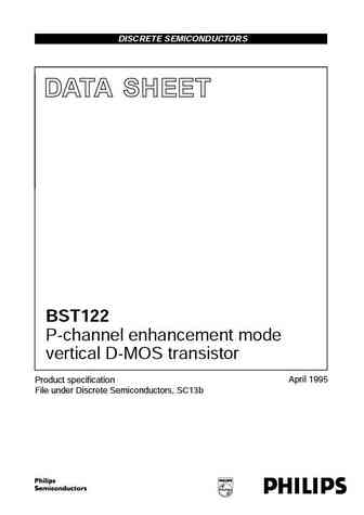
bst122 cnv 2.pdf 

DISCRETE SEMICONDUCTORS DATA SHEET BST122 P-channel enhancement mode vertical D-MOS transistor April 1995 Product specification File under Discrete Semiconductors, SC13b Philips Semiconductors Product specification P-channel enhancement mode vertical BST122 D-MOS transistor DESCRIPTION QUICK REFERENCE DATA P-channel vertical D-MOS transistor Drain-source voltage -VDS max. 60 V i... See More ⇒
0.3. Size:787K oriental semi
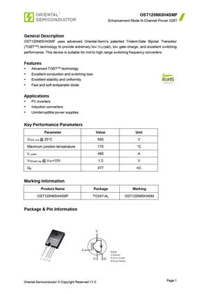
ost120n65h4smf.pdf 

OST120N65H4SMF Enhancement Mode N-Channel Power IGBT General Description OST120N65H4SMF uses advanced Oriental-Semi s patented Trident-Gate Bipolar Transistor (TGBTTM) technology to provide extremely low V (sat), low gate charge, and excellent switching CE performance. This device is suitable for mid to high range switching frequency converters. Features Advanced TGBTTM tec... See More ⇒
0.4. Size:767K oriental semi
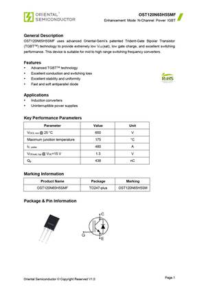
ost120n65h5smf.pdf 

OST120N65H5SMF Enhancement Mode N-Channel Power IGBT General Description OST120N65H5SMF uses advanced Oriental-Semi s patented Trident-Gate Bipolar Transistor (TGBTTM) technology to provide extremely low V (sat), low gate charge, and excellent switching CE performance. This device is suitable for mid to high range switching frequency converters. Features Advanced TGBTTM tec... See More ⇒
0.5. Size:774K oriental semi
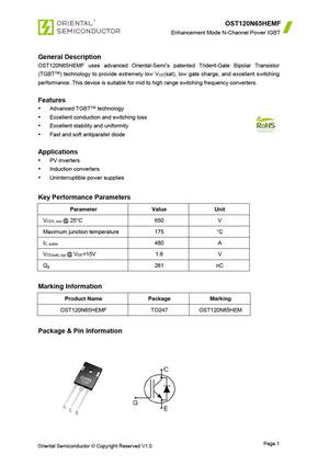
ost120n65hemf.pdf 

OST120N65HEMF Enhancement Mode N-Channel Power IGBT General Description OST120N65HEMF uses advanced Oriental-Semi s patented Trident-Gate Bipolar Transistor (TGBTTM) technology to provide extremely low V (sat), low gate charge, and excellent switching CE performance. This device is suitable for mid to high range switching frequency converters. Features Advanced TGBTTM techn... See More ⇒
0.6. Size:813K oriental semi
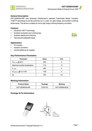
ost120n65h4umf.pdf 

OST120N65H4UMF Enhancement Mode N-Channel Power IGBT General Description OST120N65H4UMF uses advanced Oriental-Semi s patented Trident-Gate Bipolar Transistor (TGBTTM) technology to provide extremely low V (sat), low gate charge, and excellent switching CE performance. This device is suitable for mid to high range switching frequency converters. Features Advanced TGBTTM tec... See More ⇒
0.7. Size:136K powersem
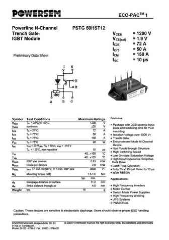
pstg50hst12.pdf 

ECO-PACTM 1 Powerline N-Channel PSTG 50HST12 Trench Gate- VCES = 1200 V IGBT Module VCE(sat) = 1.9 V IC25 = 72 A IC75 = 50 A ICM = 150 A Preliminary Data Sheet tSC = 10 s I N H M B G A Features Symbol Test Conditions Maximum Ratings TVJ = 25 C to 150 C 1200 V VCES Package with DCB ceramic base continous V VGES 20 plate and soldering pins for PCB ... See More ⇒
0.8. Size:140K powersem
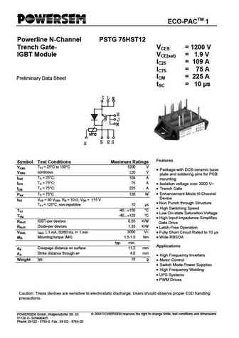
pstg75hst12.pdf 

ECO-PACTM 1 Powerline N-Channel PSTG 75HST12 Trench Gate- VCES = 1200 V IGBT Module VCE(sat) = 1.9 V IC25 = 109 A IC75 = 75 A ICM = 225 A Preliminary Data Sheet tSC = 10 s I L N H J M B E G A Features Symbol Test Conditions Maximum Ratings TVJ = 25 C to 150 C 1200 V VCES Package with DCB ceramic base continous V VGES 20 plate and soldering p... See More ⇒
0.9. Size:572K stansontech
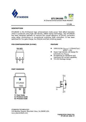
st12n10d.pdf 

ST12N10D N Channel Enhancement Mode MOSFET 12.0A DESCRIPTION ST12N10D is the N-Channel logic enhancement mode power field effect transistor which is produced using high cell density, DMOS trench technology. The ST12N10D has been designed specially to improve the overall efficiency of DC/DC converters using either synchronous or conventional switching PWM controllers. It has been... See More ⇒
0.10. Size:905K cn vbsemi
st12n10d.pdf 

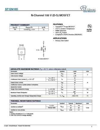
ST12N10D www.VBsemi.tw N-Channel 100 V (D-S) MOSFET FEATURES PRODUCT SUMMARY TrenchFET Power MOSFET VDS (V) RDS(on) ( )ID (A) 175 C Junction Temperature 100 0.11 4 at VGS = 10 V 15 PWM Optimized 100 % Rg Tested Compliant to RoHS Directive 2002/95/EC APPLICATIONS Primary Side Switch D TO-252 G S G D S N-Channel MOSFET ABSOLUTE MAXIMUM RATINGS... See More ⇒
Detailed specifications: SS9015, SS9016, SS9018, ST03, ST10, ST1026, ST1050, ST11, 2N3904, ST1290, ST13, ST14, ST150, ST1504, ST1505, ST1523, ST1524
Keywords - ST12 pdf specs
ST12 cross reference
ST12 equivalent finder
ST12 pdf lookup
ST12 substitution
ST12 replacement

