2N52 Specs and Replacement
Type Designator: 2N52
Material of Transistor: Ge
Polarity: PNP
Absolute Maximum Ratings
Maximum Collector Power Dissipation (Pc): 0.12 W
Maximum Collector-Base Voltage |Vcb|: 50 V
Maximum Collector-Emitter Voltage |Vce|: 50 V
Maximum Collector Current |Ic max|: 0.008 A
Max. Operating Junction Temperature (Tj): 60 °C
Electrical Characteristics
Transition Frequency (ft): 2.1 MHz
Forward Current Transfer Ratio (hFE), MIN: 1.5
Package: X016
2N52 Substitution
- BJT ⓘ Cross-Reference Search
2N52 datasheet
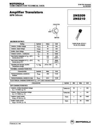
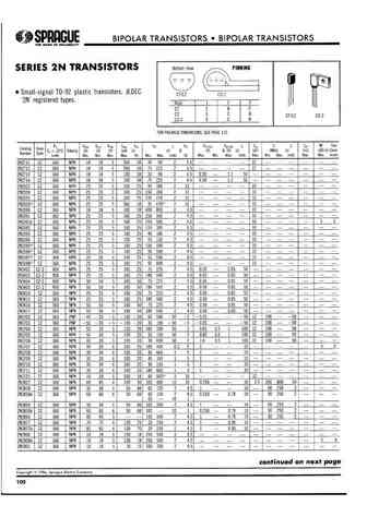
MOTOROLA Order this document SEMICONDUCTOR TECHNICAL DATA by 2N5209/D Amplifier Transistors NPN Silicon 2N5209 2N5210 COLLECTOR 3 2 BASE 1 EMITTER 1 2 3 MAXIMUM RATINGS CASE 29 04, STYLE 1 Rating Symbol Value Unit TO 92 (TO 226AA) Collector Emitter Voltage VCEO 50 Vdc Collector Base Voltage VCBO 50 Vdc Emitter Base Voltage VEBO 4.0 Vdc Collector Current C... See More ⇒
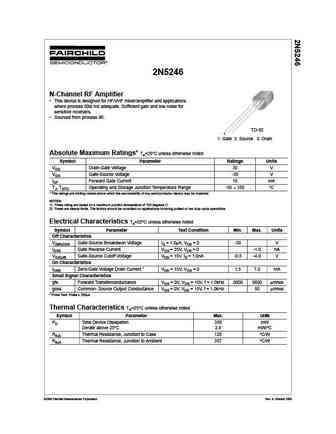
2N5246 N-Channel RF Amplifier This device is designed for HF/VHF mixer/amplifier and applications where process 50is not adequate. Sufficient gain and low noise for sensitive receivers. Sourced from process 90. TO-92 1 1. Gate 2. Source 3. Drain Absolute Maximum Ratings* Ta=25 C unless otherwise noted Symbol Parameter Ratings Units VDG Drain-Gate Voltage 30 V VGS Gate-So... See More ⇒
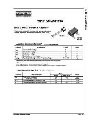
2N5210/MMBT5210 NPN General Purpose Amplifier C This device is designed for low noise, high gain, general purpose amplifier applications at collector currents from 1 A to 50 mA. E C TO-92 BE B SOT-23 Mark 3M Absolute Maximum Ratings* TA = 25 C unless otherwise noted Symbol Parameter Value Units VCEO Collector-Emitter Voltage 50 V VCBO Collector-Base Voltage 50 V VEBO Emitter-B... See More ⇒

2N5245 N-Channel RF Amplifier This device is designed for HF/VHF mixer/amplifier and applications where process 50is not adequate. Sufficient gain and low noise for sensitive receivers. Sourced from process 90. TO-92 1 1. Gate 2. Source 3. Drain Absolute Maximum Ratings* Ta=25 C unless otherwise noted Symbol Parameter Ratings Units VDG Drain-Gate Voltage 30 V VGS Gate-So... See More ⇒
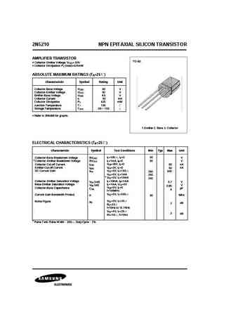
2N5210 NPN EPITAXIAL SILICON TRANSISTOR AMPLIFIER TRANSISTOR TO-92 Collector-Emitter Voltage VCEO= 50V Collector Dissipation PC (max)=625mW ABSOLUTE MAXIMUM RATINGS (T =25 ) A Characteristic Symbol Rating Unit Collector-Base Voltage VCBO 50 V Collector-Emitter Voltage VCEO 50 V Emitter-Base Voltage VEBO 4.5 V Collector Current IC 50 mA Collector Dissipation PC 625 mW Jun... See More ⇒
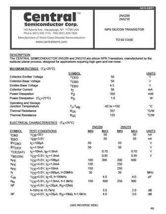
DATA SHEET 2N5209 2N5210 NPN SILICON TRANSISTOR TO-92 CASE DESCRIPTION The CENTRAL SEMICONDUCTOR 2N5209 and 2N5210 are silicon NPN Transistors, manufactured by the epitaxial planar process, designed for applications requiring high gain and low noise. MAXIMUM RATINGS (TA=25 C) SYMBOL UNITS Collector-Emitter Voltage VCEO 50 V Collector-Base Voltage VCBO 50 V Emitter-Base V... See More ⇒
145 Adams Avenue, Hauppauge, NY 11788 USA Tel (631) 435-1110 Fax (631) 435-1824 ... See More ⇒
145 Adams Avenue, Hauppauge, NY 11788 USA Tel (631) 435-1110 Fax (631) 435-1824 ... See More ⇒
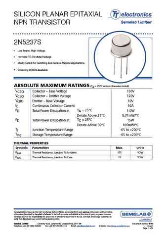
SILICON PLANAR EPITAXIAL NPN TRANSISTOR 2N5237S Low Power, High Voltage. Hermetic TO-39 Metal Package. Ideally Suited For Switching And General Purpose Applications. Screening Options Available ABSOLUTE MAXIMUM RATINGS (TA = 25 C unless otherwise stated) VCBO Collector Base Voltage 150V VCEO Collector Emitter Voltage 120V VEBO Emitter Base ... See More ⇒
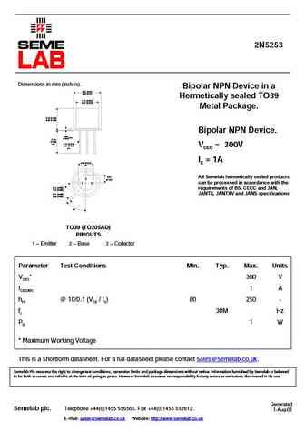
2N5253 Dimensions in mm (inches). Bipolar NPN Device in a 8.51 (0.34) 9.40 (0.37) Hermetically sealed TO39 7.75 (0.305) 8.51 (0.335) Metal Package. 6.10 (0.240) 6.60 (0.260) Bipolar NPN Device. 0.89 max. (0.035) 12.70 (0.500) min. 0.41 (0.016) 0.53 (0.021) VCEO = 300V dia. IC = 1A 5.08 (0.200) typ. 2.54 All Semelab hermetically sealed products 2 (0.100) 1 3... See More ⇒

2N5252 Dimensions in mm (inches). Bipolar NPN Device in a 8.51 (0.34) 9.40 (0.37) Hermetically sealed TO39 7.75 (0.305) 8.51 (0.335) Metal Package. 6.10 (0.240) 6.60 (0.260) Bipolar NPN Device. 0.89 max. (0.035) 12.70 (0.500) min. 0.41 (0.016) 0.53 (0.021) VCEO = 300V dia. IC = 1A 5.08 (0.200) typ. 2.54 All Semelab hermetically sealed products 2 (0.100) 1 3... See More ⇒
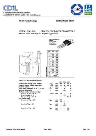
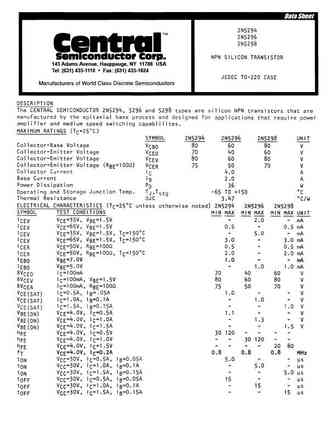
Continental Device India Limited An ISO/TS 16949, ISO 9001 and ISO 14001 Certified Company TO-220 Plastic Package 2N5294, 2N5296, 2N5298 2N5294, 5296, 5298 NPN PLASTIC POWER TRANSISTORS Medium Power Switching and Amplifier Applications PIN CONFIGURATION 4 1. BASE 2. COLLECTOR 3. EMITTER 4. COLLECTOR 1 2 3 C DIM MIN. MAX. B E F A 14.42 16.51 B 9.63 10.67 C 3.56 4.83 D0.90 E... See More ⇒
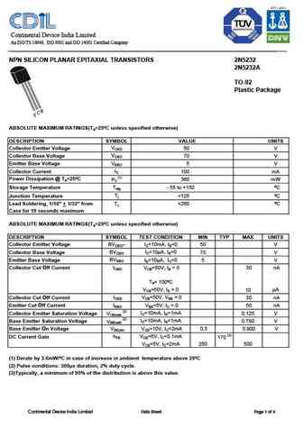
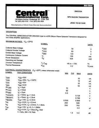
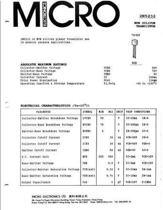
Continental Device India Limited An ISO/TS 16949, ISO 9001 and ISO 14001 Certified Company NPN SILICON PLANAR EPITAXIAL TRANSISTORS 2N5232 2N5232A TO-92 Plastic Package ABSOLUTE MAXIMUM RATINGS(Ta=25 C unless specified otherwise) DESCRIPTION SYMBOL VALUE UNITS VCEO Collector Emitter Voltage 50 V VCBO Collector Base Voltage 70 V VEBO Emitter Base Voltage 5V IC Collector Current 1... See More ⇒
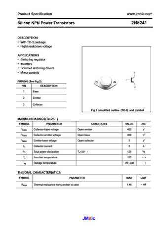
Product Specification www.jmnic.com Silicon NPN Power Transistors 2N5241 DESCRIPTION With TO-3 package High breakdown voltage APPLICATIONS Switching regulator Inverters Solenoid and relay drivers Motor controls PINNING (See Fig.2) PIN DESCRIPTION 1 Base 2 Emitter 3 Collector Fig.1 simplified outline (TO-3) and symbol MAXIMUN RATINGS(Ta=25 ) SYMBOL PA... See More ⇒
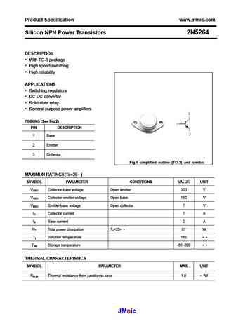
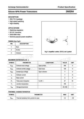
Product Specification www.jmnic.com Silicon NPN Power Transistors 2N5264 DESCRIPTION With TO-3 package High speed switching High reliability APPLICATIONS Switching regulators DC-DC convertor Solid state relay General purpose power amplifiers PINNING (See Fig.2) PIN DESCRIPTION 1 Base 2 Emitter 3 Collector Fig.1 simplified outline (TO-3) and symbol MA... See More ⇒
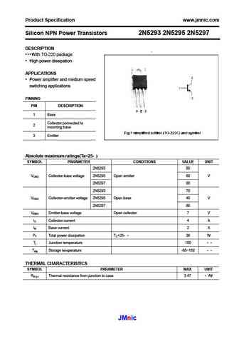
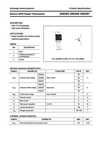
Product Specification www.jmnic.com Silicon NPN Power Transistors 2N5293 2N5295 2N5297 DESCRIPTION With TO-220 package High power dissipation APPLICATIONS Power amplifier and medium speed switching applications PINNING PIN DESCRIPTION 1 Base Collector;connected to 2 mounting base 3 Emitter Absolute maximum ratings(Ta=25 ) SYMBOL PARAMETER CONDITIONS VA... See More ⇒
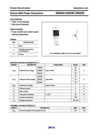
Product Specification www.jmnic.com Silicon NPN Power Transistors 2N5294 2N5296 2N5298 DESCRIPTION With TO-220 package High power dissipation APPLICATIONS Power amplifier and medium speed switching applications PINNING PIN DESCRIPTION 1 Base Collector;connected to 2 mounting base 3 Emitter Absolute maximum ratings(Ta=25 ) SYMBOL PARAMETER CONDITIONS VAL... See More ⇒
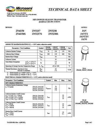
TECHNICAL DATA SHEET 6 Lake Street, Lawrence, MA 01841 1-800-446-1158 / (978) 620-2600 / Fax (978) 689-0803 Website http //www.microsemi.com NPN POWER SILICON TRANSISTOR Qualified per MIL-PRF-19500/394 DEVICES LEVELS JAN 2N4150 2N5237 2N5238 JANTX 2N4150S 2N5237S 2N5238S JANTXV JANS ABSOLUTE MAXIMUM RATINGS (TC = +25 C unless otherwise noted) 2N4150 2N5237 2N5238... See More ⇒
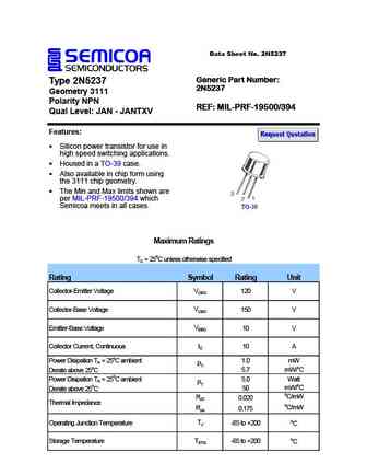
Data Sheet No. 2N5237 Generic Part Number Type 2N5237 2N5237 Geometry 3111 Polarity NPN REF MIL-PRF-19500/394 Qual Level JAN - JANTXV Features Silicon power transistor for use in high speed switching applications. Housed in a TO-39 case. Also available in chip form using the 3111 chip geometry. The Min and Max limits shown are per MIL-PRF-19500/394 which Semi... See More ⇒
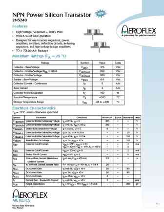
NPN Power Silicon Transistor 2N5240 Features High Voltage Vceo(sus) = 300 V (min) Wide Area of Safe Operation Designed for use in series regulators, power amplifiers, inverters, deflection circuits, switching regulators, and high-voltage bridge amplifiers. TO-3 (TO-204AA) Package Maximum Ratings (TA = 25 C) Ratings Symbol Value Units Collector - Base Voltage VCBO... See More ⇒
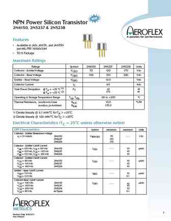
NPN Power Silicon Transistor 2N4150, 2N5237 & 2N5238 Features Available in JAN, JANTX, and JANTXV per MIL-PRF-19500/384 TO-5 Package Maximum Ratings Ratings Symbol 2N4150 2N5237 2N5238 Units Collector - Emitter Voltage VCEO 70 120 170 Vdc Collector - Base Voltage VCBO 100 150 200 Vdc Emitter - Base Voltage VEBO 10.0 Vdc Collector Current IC 4.0 Adc Total Power Dissipation @ ... See More ⇒
... See More ⇒
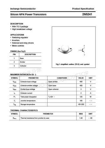
Inchange Semiconductor Product Specification Silicon NPN Power Transistors 2N5241 DESCRIPTION With TO-3 package High breakdown voltage APPLICATIONS Switching regulator Inverters Solenoid and relay drivers Motor controls PINNING (See Fig.2) PIN DESCRIPTION 1 Base 2 Emitter Fig.1 simplified outline (TO-3) and symbol 3 Collector MAXIMUN RATINGS(Ta=25 ) ... See More ⇒
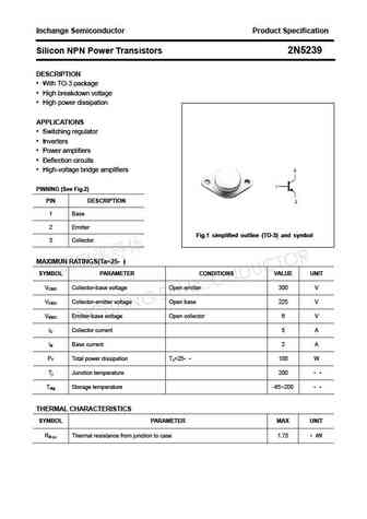
Inchange Semiconductor Product Specification Silicon NPN Power Transistors 2N5239 DESCRIPTION With TO-3 package High breakdown voltage High power dissipation APPLICATIONS Switching regulator Inverters Power amplifiers Deflection circuits High-voltage bridge amplifiers PINNING (See Fig.2) PIN DESCRIPTION 1 Base 2 Emitter Fig.1 simplified outline (TO-... See More ⇒
Inchange Semiconductor Product Specification Silicon NPN Power Transistors 2N5264 DESCRIPTION With TO-3 package High speed switching High reliability APPLICATIONS Switching regulators DC-DC convertor Solid state relay General purpose power amplifiers PINNING (See Fig.2) PIN DESCRIPTION 1 Base 2 Emitter Fig.1 simplified outline (TO-3) and symbol 3 Coll... See More ⇒
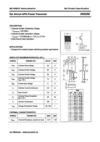
INCHANGE Semiconductor isc Product Specification isc Silicon NPN Power Transistor 2N5298 DESCRIPTION Collector-Emitter Sustaining Voltage- VCEO(SUS) = 60V(Min) Collector-Emitter Saturation Voltage- VCE(sat) = 1.0V(Max)@ IC= 1.5A, IB= 0.15A Wide Area of Safe Operation APPLICATIONS Designed for medium power switching amplifier applications. ABSOLUTE MAXIMUM RATING... See More ⇒
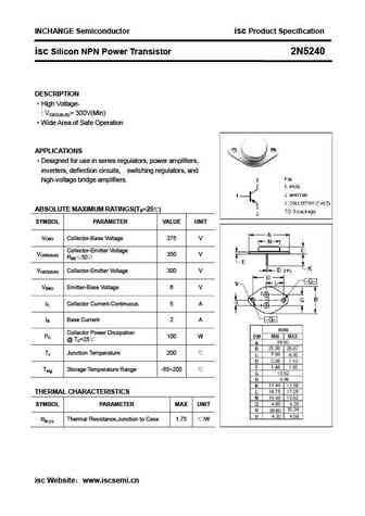
INCHANGE Semiconductor isc Product Specification isc Silicon NPN Power Transistor 2N5240 DESCRIPTION High Voltage- VCEO(SUS)= 300V(Min) Wide Area of Safe Operation APPLICATIONS Designed for use in series regulators, power amplifiers, inverters, deflection circuits, switching regulators, and high-voltage bridge amplifiers. ABSOLUTE MAXIMUM RATINGS(Ta=25 ) SYMBOL... See More ⇒
Inchange Semiconductor Product Specification Silicon NPN Power Transistors 2N5293 2N5295 2N5297 DESCRIPTION With TO-220 package High power dissipation APPLICATIONS Power amplifier and medium speed switching applications PINNING PIN DESCRIPTION 1 Base Collector;connected to 2 mounting base 3 Emitter Absolute maximum ratings(Ta=25 ) SYMBOL PARAMETER CONDITIO... See More ⇒
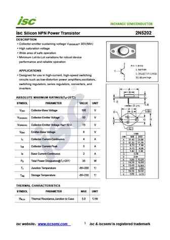
isc Silicon NPN Power Transistor 2N5202 DESCRIPTION Collector-emitter sustaining voltage V = 90V(Min) CEO(SUS) High saturation voltage Wide area of safe operation Minimum Lot-to-Lot variations for robust device performance and reliable operation APPLICATIONS Designed for use in high-current, high-speed switching circuits such as low-distortion power amplifiers,oscillators, ... See More ⇒
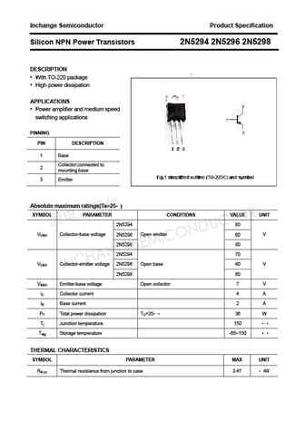
Inchange Semiconductor Product Specification Silicon NPN Power Transistors 2N5294 2N5296 2N5298 DESCRIPTION With TO-220 package High power dissipation APPLICATIONS Power amplifier and medium speed switching applications PINNING PIN DESCRIPTION 1 Base Collector;connected to 2 mounting base 3 Emitter Absolute maximum ratings(Ta=25 ) SYMBOL PARAMETER CONDITIO... See More ⇒
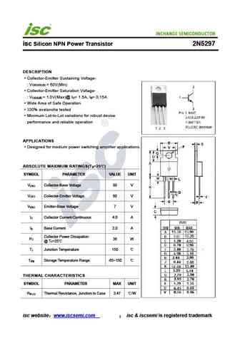
isc Silicon NPN Power Transistor 2N5297 DESCRIPTION Collector-Emitter Sustaining Voltage- V = 60V(Min) CEO(SUS) Collector-Emitter Saturation Voltage- V = 1.0V(Max)@ I = 1.5A, I = 0.15A CE(sat) C B Wide Area of Safe Operation 100% avalanche tested Minimum Lot-to-Lot variations for robust device performance and reliable operation APPLICATIONS Designed for medium power... See More ⇒
Detailed specifications: 2N519, 2N5190, 2N5191, 2N5192, 2N5193, 2N5194, 2N5195, 2N519A, 2SA1943, 2N520, 2N5200, 2N5201, 2N5202, 2N5203, 2N5208, 2N5209, 2N520A
Keywords - 2N52 pdf specs
2N52 cross reference
2N52 equivalent finder
2N52 pdf lookup
2N52 substitution
2N52 replacement
🌐 : EN ES РУ

LIST
Last Update
BJT: GA1A4M | SBT42 | 2SA200-Y | 2SA200-O | 2SD882-Q | 2SD882-P
Popular searches
2sa794 | 2sa816 | 2sc897 datasheet | 2sd389 | mp41 transistor | nkt275 datasheet | 2sd947 | a763 transistor