2N5241 Specs and Replacement
Type Designator: 2N5241
Material of Transistor: Si
Polarity: NPN
Absolute Maximum Ratings
Maximum Collector Power Dissipation (Pc): 125 W
Maximum Collector-Base Voltage |Vcb|: 400 V
Maximum Collector-Emitter Voltage |Vce|: 325 V
Maximum Emitter-Base Voltage |Veb|: 5 V
Maximum Collector Current |Ic max|: 5 A
Max. Operating Junction Temperature (Tj): 150 °C
Electrical Characteristics
Transition Frequency (ft): 2.5 MHz
Forward Current Transfer Ratio (hFE), MIN: 15
Package: TO3
2N5241 Substitution
- BJT ⓘ Cross-Reference Search
2N5241 datasheet
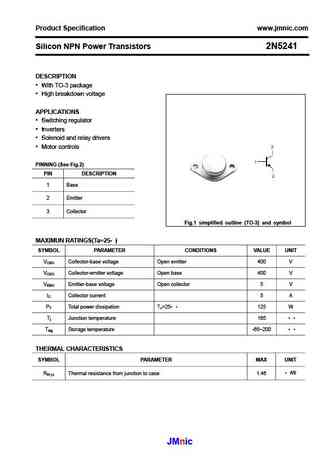
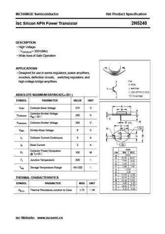
Product Specification www.jmnic.com Silicon NPN Power Transistors 2N5241 DESCRIPTION With TO-3 package High breakdown voltage APPLICATIONS Switching regulator Inverters Solenoid and relay drivers Motor controls PINNING (See Fig.2) PIN DESCRIPTION 1 Base 2 Emitter 3 Collector Fig.1 simplified outline (TO-3) and symbol MAXIMUN RATINGS(Ta=25 ) SYMBOL PA... See More ⇒
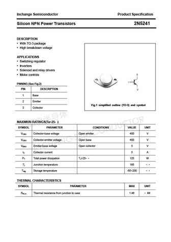
Inchange Semiconductor Product Specification Silicon NPN Power Transistors 2N5241 DESCRIPTION With TO-3 package High breakdown voltage APPLICATIONS Switching regulator Inverters Solenoid and relay drivers Motor controls PINNING (See Fig.2) PIN DESCRIPTION 1 Base 2 Emitter Fig.1 simplified outline (TO-3) and symbol 3 Collector MAXIMUN RATINGS(Ta=25 ) ... See More ⇒
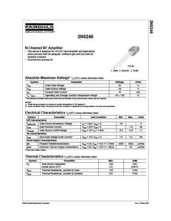
2N5246 N-Channel RF Amplifier This device is designed for HF/VHF mixer/amplifier and applications where process 50is not adequate. Sufficient gain and low noise for sensitive receivers. Sourced from process 90. TO-92 1 1. Gate 2. Source 3. Drain Absolute Maximum Ratings* Ta=25 C unless otherwise noted Symbol Parameter Ratings Units VDG Drain-Gate Voltage 30 V VGS Gate-So... See More ⇒

2N5245 N-Channel RF Amplifier This device is designed for HF/VHF mixer/amplifier and applications where process 50is not adequate. Sufficient gain and low noise for sensitive receivers. Sourced from process 90. TO-92 1 1. Gate 2. Source 3. Drain Absolute Maximum Ratings* Ta=25 C unless otherwise noted Symbol Parameter Ratings Units VDG Drain-Gate Voltage 30 V VGS Gate-So... See More ⇒
Detailed specifications: 2N5235, 2N5236, 2N5237, 2N5238, 2N5239, 2N523A, 2N524, 2N5240, 2SC2655, 2N5242, 2N5243, 2N5244, 2N5249, 2N5249A, 2N524A, 2N525, 2N5250
Keywords - 2N5241 pdf specs
2N5241 cross reference
2N5241 equivalent finder
2N5241 pdf lookup
2N5241 substitution
2N5241 replacement
🌐 : EN ES РУ

LIST
Last Update
BJT: GA1A4M | SBT42 | 2SA200-Y
Popular searches
13009 datasheet | 3dd15d transistor | pa110bda | 2sb1243 | a1123 transistor | skd502t datasheet | svf7n65f | 2sc1419 datasheet