2N5292 Datasheet. Specs and Replacement
Type Designator: 2N5292 📄📄
Material of Transistor: Si
Polarity: PNP
Absolute Maximum Ratings
Maximum Collector Power Dissipation (Pc): 0.36 W
Maximum Collector-Base Voltage |Vcb|: 12 V
Maximum Collector-Emitter Voltage |Vce|: 12 V
Maximum Emitter-Base Voltage |Veb|: 4 V
Maximum Collector Current |Ic max|: 0.1 A
Max. Operating Junction Temperature (Tj): 200 °C
Electrical Characteristics
Transition Frequency (ft): 800 MHz
Collector Capacitance (Cc): 4.5 pF
Forward Current Transfer Ratio (hFE), MIN: 40
Package: TO18
📄📄 Copy
2N5292 Substitution
- BJT ⓘ Cross-Reference Search
2N5292 datasheet
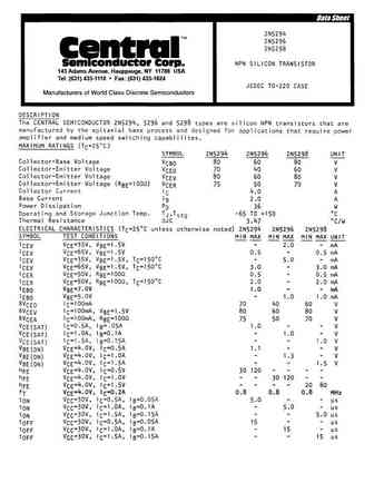
145 Adams Avenue, Hauppauge, NY 11788 USA Tel (631) 435-1110 Fax (631) 435-1824 ... See More ⇒
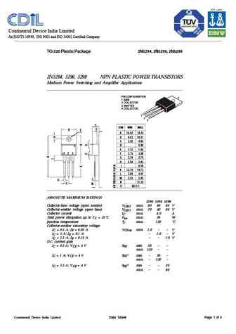
Continental Device India Limited An ISO/TS 16949, ISO 9001 and ISO 14001 Certified Company TO-220 Plastic Package 2N5294, 2N5296, 2N5298 2N5294, 5296, 5298 NPN PLASTIC POWER TRANSISTORS Medium Power Switching and Amplifier Applications PIN CONFIGURATION 4 1. BASE 2. COLLECTOR 3. EMITTER 4. COLLECTOR 1 2 3 C DIM MIN. MAX. B E F A 14.42 16.51 B 9.63 10.67 C 3.56 4.83 D0.90 E... See More ⇒
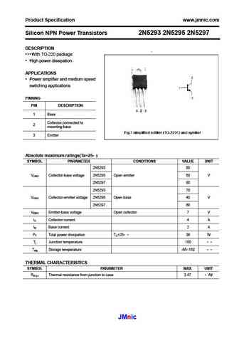
Product Specification www.jmnic.com Silicon NPN Power Transistors 2N5293 2N5295 2N5297 DESCRIPTION With TO-220 package High power dissipation APPLICATIONS Power amplifier and medium speed switching applications PINNING PIN DESCRIPTION 1 Base Collector;connected to 2 mounting base 3 Emitter Absolute maximum ratings(Ta=25 ) SYMBOL PARAMETER CONDITIONS VA... See More ⇒
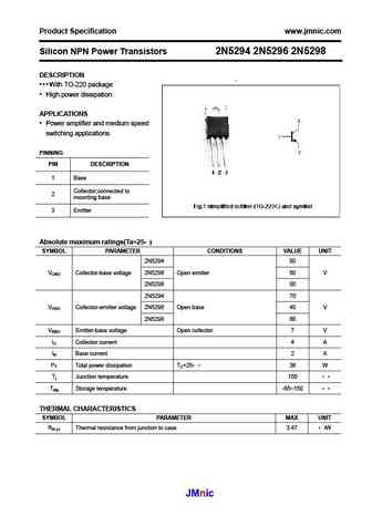
Product Specification www.jmnic.com Silicon NPN Power Transistors 2N5294 2N5296 2N5298 DESCRIPTION With TO-220 package High power dissipation APPLICATIONS Power amplifier and medium speed switching applications PINNING PIN DESCRIPTION 1 Base Collector;connected to 2 mounting base 3 Emitter Absolute maximum ratings(Ta=25 ) SYMBOL PARAMETER CONDITIONS VAL... See More ⇒
Detailed specifications: 2N5285, 2N5286, 2N5287, 2N5288, 2N5289, 2N529, 2N5290, 2N5291, C1815, 2N5293, 2N5294, 2N5295, 2N5296, 2N5297, 2N5298, 2N53, 2N530
Keywords - 2N5292 pdf specs
2N5292 cross reference
2N5292 equivalent finder
2N5292 pdf lookup
2N5292 substitution
2N5292 replacement
BJT Parameters and How They Relate
History: 2SD478 | 2N6678M3A | UN911D | DTA024EEB
🌐 : EN ES РУ
LIST
Last Update
BJT: ZDT6705 | GA1L4Z | GA1A4M | SBT42 | 2SA200-Y | 2SA200-O
Popular searches
a94 transistor | c5149 datasheet | m1830m mosfet | pkch2bb mosfet | 2024ont | 2n1306 transistor | 2sa750 datasheet | 2sa940 transistor datasheet


