2N53 Specs and Replacement
Type Designator: 2N53
Material of Transistor: Ge
Polarity: PNP
Absolute Maximum Ratings
Maximum Collector Power Dissipation (Pc): 0.1 W
Maximum Collector-Base Voltage |Vcb|: 50 V
Maximum Collector-Emitter Voltage |Vce|: 50 V
Maximum Collector Current |Ic max|: 0.008 A
Max. Operating Junction Temperature (Tj): 60 °C
Electrical Characteristics
Transition Frequency (ft): 5 MHz
Forward Current Transfer Ratio (hFE), MIN: 2
Noise Figure, dB: -
Package: X016
- BJT ⓘ Cross-Reference Search
2N53 datasheet
0.1. Size:251K motorola
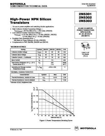
2n5301 2n5302 2n5303.pdf 

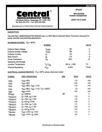
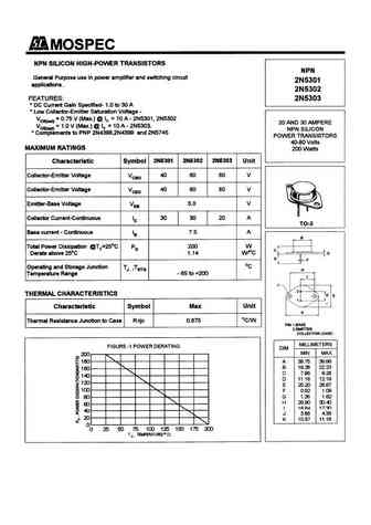
Order this document MOTOROLA by 2N5301/D SEMICONDUCTOR TECHNICAL DATA 2N5301 2N5302 High-Power NPN Silicon 2N5303 Transistors . . . for use in power amplifier and switching circuits applications. 20 AND 30 AMPERE High Collector Emitter Sustaining Voltage POWER TRANSISTORS VCEO(sus) = 80 Vdc (Min) @ IC = 200 mAdc (2N5303) NPN SILICON Low Collector Emitter Saturatio... See More ⇒
0.2. Size:44K st
2n5320.pdf 

2N5320 SMALL SIGNAL NPN TRANSISTOR DESCRIPTION The 2N5320 is a silicon Epitaxial Planar NPN transistor in Jedec TO-39 metal case. It is especially intended for high-voltage medium power application in industrial and commercial equipments. The complementary PNP type is the 2N5322 TO-39 INTERNAL SCHEMATIC DIAGRAM ABSOLUTE MAXIMUM RATINGS Symbol Parameter Value Unit VCBO Collecto... See More ⇒
0.3. Size:67K st
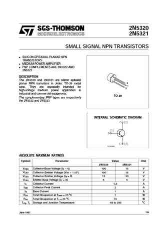
2n5320 2n5321.pdf 

2N5320 2N5321 SMALL SIGNAL NPN TRANSISTORS SILICON EPITAXIAL PLANAR NPN TRANSISTORS MEDIUM POWER AMPLIFIER PNP COMPLEMENTS ARE 2N5322 AND 2N5323 DESCRIPTION The 2N5320 and 2N5321 are silicon epitaxial planar NPN transistors in Jedec TO-39 metal case. They are especially intended for high-voltage medium power application in industrial and commercial equipments. TO-39 The compl... See More ⇒
0.4. Size:67K st
2n5322 2n5323.pdf 

2N5322 2N5323 SMALL SIGNAL PNP TRANSISTORS SILICON EPITAXIAL PLANAR PNP TRANSISTORS MEDIUM POWER AMPLIFIER NPN COMPLEMENTS ARE 2N5320 AND 2N5321 DESCRIPTION The 2N5322 and 2N5323 are silicon epitaxial planar PNP transistors in Jedec TO-39 metal case. They are especially intended for high-voltage medium power application in industrial and commercial equipments. TO-39 The compl... See More ⇒
0.5. Size:44K st
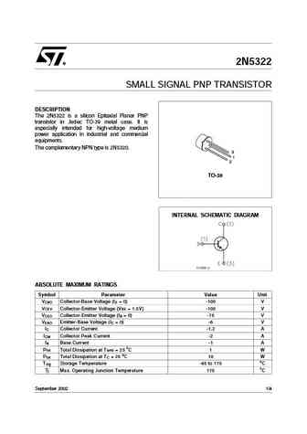
2n5322.pdf 

2N5322 SMALL SIGNAL PNP TRANSISTOR DESCRIPTION The 2N5322 is a silicon Epitaxial Planar PNP transistor in Jedec TO-39 metal case. It is especially intended for high-voltage medium power application in industrial and commercial equipments. The complementary NPN type is 2N5320. TO-39 INTERNAL SCHEMATIC DIAGRAM ABSOLUTE MAXIMUM RATINGS Symbol Parameter Value Unit VCBO Collector-B... See More ⇒
0.6. Size:60K fairchild semi
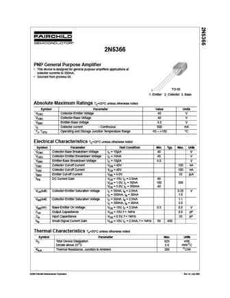
2n5366.pdf 

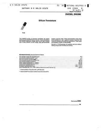
2N5366 PNP General Purpose Amplifier This device is designed for general purpose amplifiers applications at collector currents to 300mA. Sourced from process 68. TO-92 1 1. Emitter 2. Collector 3. Base Absolute Maximum Ratings TC=25 C unless otherwise noted Symbol Parameter Value Units VCEO Collector-Emitter Voltage 40 V VCBO Collector-Base Voltage 40 V VEBO Emitter-Base ... See More ⇒
0.7. Size:56K fairchild semi
2n5306.pdf 

2N5306 NPN Darlington Transistor This device is designed for applications requiring extremely high current gain at currents to 1.0A. Sourced from process 05. See MPSA14 for characteristics. TO-92 1 1. Emitter 2. Collector 3. Base Absolute Maximum Ratings * TA=25 C unless otherwise noted Symbol Parameter Value Units VCEO Collector-Emitter Voltage 25 V VCBO Collector-Bas... See More ⇒
0.8. Size:56K fairchild semi
2n5308.pdf 

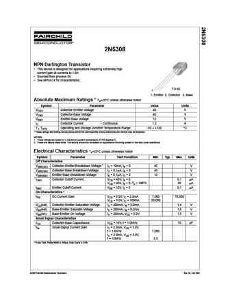
2N5308 NPN Darlington Transistor This device is designed for applications requiring extremely high current gain at currents to 1.0A. Sourced from process 05. See MPSA14 for characteristics. TO-92 1 1. Emitter 2. Collector 3. Base Absolute Maximum Ratings * TA=25 C unless otherwise noted Symbol Parameter Value Units VCEO Collector-Emitter Voltage 40 V VCBO Collector-Bas... See More ⇒
0.9. Size:57K fairchild semi
2n5307.pdf 

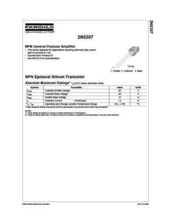
2N5307 NPN General Purpose Amplifier This device designed for applications requiring extremely high current gain at currents to 1.0A. Sourced from Process 05. See MPSA14 for characteristics. TO-92 1 1. Emitter 2. Collector 3. Base NPN Epitaxial Silicon Transistor Absolute Maximum Ratings* Ta=25 C unless otherwise noted Symbol Parameter Value Units VCEO Collector-Emit... See More ⇒
0.10. Size:95K central
2n5303.pdf 

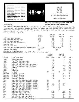
145 Adams Avenue, Hauppauge, NY 11788 USA Tel (631) 435-1110 Fax (631) 435-1824 TM Central Semiconductor Corp. 145 Adams Avenue Hauppauge, NY 11788 USA Tel (631) 435-1110 Fax (631) 435-1824 www.centralsemi.com ... See More ⇒
0.11. Size:110K central
2n5320 2n5321 2n5322 2n5323.pdf 

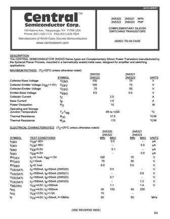
DATA SHEET 2N5320 2N5321 NPN 2N5322 2N5323 PNP COMPLEMENTARY SILICON SWITCHING TRANSISTORS JEDEC TO-39 CASE DESCRIPTION The CENTRAL SEMICONDUCTOR 2N5320 Series types are Complementary Silicon Power Transistors manufactured by the Epitaxial Planar Process, mounted in a hermetically sealed metal case, designed for amplifier and switching applications. MAXIMUM RATINGS (TC=25 C ... See More ⇒
0.13. Size:92K onsemi
2n5302.pdf 

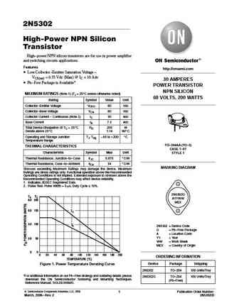
2N5302 High-Power NPN Silicon Transistor High-power NPN silicon transistors are for use in power amplifier and switching circuits applications. Features http //onsemi.com Low Collector-Emitter Saturation Voltage - VCE(sat) = 0.75 Vdc (Max) @ IC = 10 Adc 30 AMPERES Pb-Free Package is Available* POWER TRANSISTOR NPN SILICON MAXIMUM RATINGS (Note 1) (TJ = 25 C unless otherwis... See More ⇒
0.14. Size:92K onsemi
2n5302g.pdf 

2N5302 High-Power NPN Silicon Transistor High-power NPN silicon transistors are for use in power amplifier and switching circuits applications. Features http //onsemi.com Low Collector-Emitter Saturation Voltage - VCE(sat) = 0.75 Vdc (Max) @ IC = 10 Adc 30 AMPERES Pb-Free Package is Available* POWER TRANSISTOR NPN SILICON MAXIMUM RATINGS (Note 1) (TJ = 25 C unless otherwis... See More ⇒
0.18. Size:59K semelab
2n5320x.pdf 

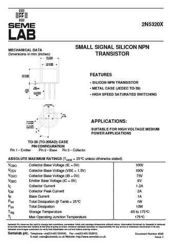
2N5320X SMALL SIGNAL SILICON NPN MECHANICAL DATA Dimensions in mm (inches) TRANSISTOR 8.51 (0.34) 9.40 (0.37) 7.75 (0.305) 8.51 (0.335) 6.10 (0.240) FEATURES 6.60 (0.260) SILICON NPN TRANSISTOR 0.89 (0.035)max. METAL CASE (JEDEC TO-39) 12.70 (0.500) 0.41 (0.016) min. 0.53 (0.021) HIGH SPEED SATURATED SWITCHING dia. 5.08 (0.200) typ. 2.54 2 (0.100)... See More ⇒
0.19. Size:20K semelab
2n5338lcc4.pdf 

2N5339LCC4 MECHANICAL DATA Dimensions in mm (inches) NPN SILICON TRANSISTORS 9.14 (0.360) 1.27 (0.050) 8.64 (0.340) 1.07 (0.040) 2.16 (0.085) 12 13 14 15 16 1.39 (0.055) 1.02 (0.040) 11 17 10 18 7.62 (0.300) 7.12 (0.280) 9 1 0.76 (0.030) FEATURES 8 2 0.51 (0.020) Hermetically sealed ceramic surface 0.33 (0.013) Rad. 0.08 (0.003) 7 6 5 4 3 mount package 0.43 (0... See More ⇒
0.20. Size:11K semelab
2n5333.pdf 

2N5333 Dimensions in mm (inches). Bipolar PNP Device in a 8.51 (0.34) 9.40 (0.37) Hermetically sealed TO39 7.75 (0.305) 8.51 (0.335) Metal Package. 6.10 (0.240) 6.60 (0.260) Bipolar PNP Device. 0.89 max. (0.035) 12.70 (0.500) min. 0.41 (0.016) 0.53 (0.021) VCEO = 80V dia. IC = 2A 5.08 (0.200) typ. 2.54 All Semelab hermetically sealed products 2 (0.100) 1 3 ... See More ⇒
0.21. Size:11K semelab
2n5334.pdf 

2N5334 Dimensions in mm (inches). Bipolar NPN Device in a 8.51 (0.34) 9.40 (0.37) Hermetically sealed TO39 7.75 (0.305) 8.51 (0.335) Metal Package. 6.10 (0.240) 6.60 (0.260) Bipolar NPN Device. 0.89 max. (0.035) 12.70 (0.500) min. 0.41 (0.016) 0.53 (0.021) VCEO = 60V dia. IC = 3A 5.08 (0.200) typ. 2.54 All Semelab hermetically sealed products 2 (0.100) 1 3 ... See More ⇒
0.22. Size:20K semelab
2n5339lcc4.pdf 

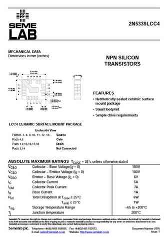
2N5339LCC4 MECHANICAL DATA Dimensions in mm (inches) NPN SILICON TRANSISTORS 9.14 (0.360) 1.27 (0.050) 8.64 (0.340) 1.07 (0.040) 2.16 (0.085) 12 13 14 15 16 1.39 (0.055) 1.02 (0.040) 11 17 10 18 7.62 (0.300) 7.12 (0.280) 9 1 0.76 (0.030) FEATURES 8 2 0.51 (0.020) Hermetically sealed ceramic surface 0.33 (0.013) Rad. 0.08 (0.003) 7 6 5 4 3 mount package 0.43 (0... See More ⇒
0.23. Size:11K semelab
2n5335.pdf 

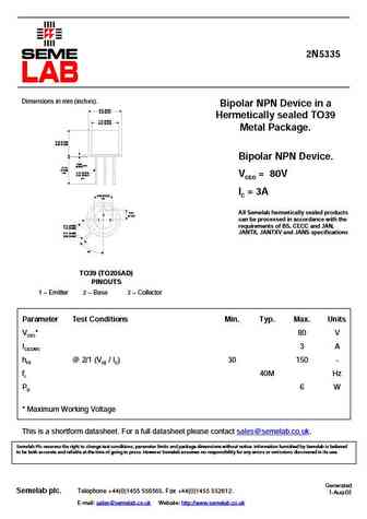
2N5335 Dimensions in mm (inches). Bipolar NPN Device in a 8.51 (0.34) 9.40 (0.37) Hermetically sealed TO39 7.75 (0.305) 8.51 (0.335) Metal Package. 6.10 (0.240) 6.60 (0.260) Bipolar NPN Device. 0.89 max. (0.035) 12.70 (0.500) min. 0.41 (0.016) 0.53 (0.021) VCEO = 80V dia. IC = 3A 5.08 (0.200) typ. 2.54 All Semelab hermetically sealed products 2 (0.100) 1 3 ... See More ⇒
0.24. Size:188K cdil
2n5320 21 22 23.pdf 

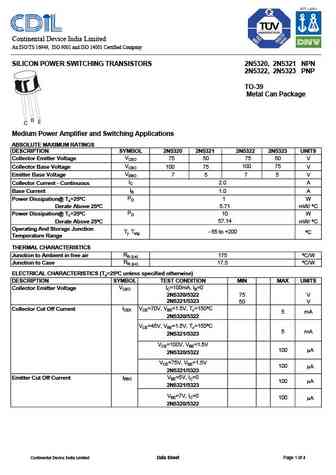
Continental Device India Limited An ISO/TS 16949, ISO 9001 and ISO 14001 Certified Company SILICON POWER SWITCHING TRANSISTORS 2N5320, 2N5321 NPN 2N5322, 2N5323 PNP TO-39 Metal Can Package Medium Power Amplifier and Switching Applications ABSOLUTE MAXIMUM RATINGS DESCRIPTION SYMBOL 2N5320 2N5321 2N5322 2N5323 UNITS VCEO Collector Emitter Voltage 75 50 75 50 V VCBO Collector Base Vol... See More ⇒
0.25. Size:91K interfet
2n5397 2n5398.pdf 

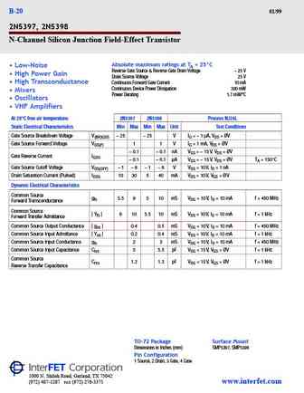
Databook.fxp 1/13/99 2 09 PM Page B-20 B-20 01/99 2N5397, 2N5398 N-Channel Silicon Junction Field-Effect Transistor Absolute maximum ratings at TA = 25 C Low-Noise Reverse Gate Source & Reverse Gate Drain Voltage 25 V High Power Gain Drain Source Voltage 25 V High Transconductance Continuous Forward Gate Current 10 mA Continuous Device Power Dissipation 300 mW Mixer... See More ⇒
0.28. Size:178K microsemi
2n5339u3.pdf 

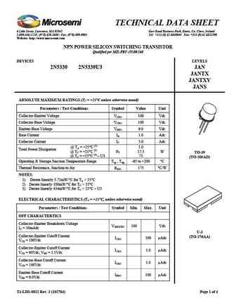
TECHNICAL DATA SHEET 6 Lake Street, Lawrence, MA 01841 Gort Road Business Park, Ennis, Co. Clare, Ireland 1-800-446-1158 / (978) 620-2600 / Fax (978) 689-0803 Tel +353 (0) 65 6840044 Fax +353 (0) 65 6822298 Website http //www.microsemi.com NPN POWER SILICON SWITCHING TRANSISTOR Qualified per MIL-PRF-19500/560 DEVICES LEVELS 2N5339 2N5339U3 JAN JANTX JANTXV JANS ABSOLUTE MA... See More ⇒
0.29. Size:159K aeroflex
2n5339.pdf 

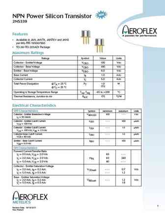
NPN Power Silicon Transistor 2N5339 Features Available in JAN, JANTX, JANTXV and JANS per MIL-PRF-19500/560 TO-39 (TO-205AD) Package Maximum Ratings Ratings Symbol Value Units Collector - Emitter Voltage VCEO 100 Vdc Collector - Base Voltage VCBO 100 Vdc Emitter - Base Voltage VEBO 6.0 Vdc Base Current IB 1.0 Adc Collector Current IC 5.0 Adc Total Power Dissipation @ TA = 2... See More ⇒
0.32. Size:167K cn sptech
2n5301.pdf 

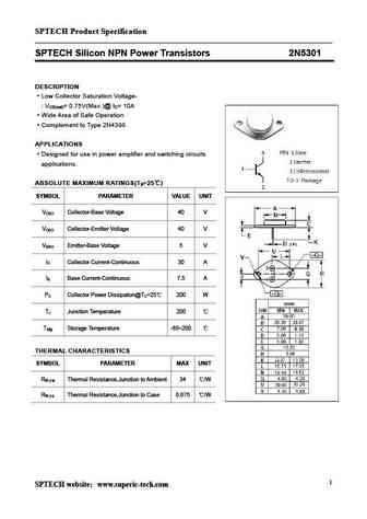
SPTECH Product Specification SPTECH Silicon NPN Power Transistors 2N5301 DESCRIPTION Low Collector Saturation Voltage- V = 0.75V(Max.)@ I = 10A CE(sat) C Wide Area of Safe Operation Complement to Type 2N4398 APPLICATIONS Designed for use in power amplifier and switching circuits applications. ABSOLUTE MAXIMUM RATINGS(T =25 ) a SYMBOL PARAMETER VALUE UNIT V Collector-Ba... See More ⇒
0.33. Size:167K cn sptech
2n5302.pdf 

SPTECH Product Specification SPTECH Silicon NPN Power Transistors 2N5302 DESCRIPTION Low Collector Saturation Voltage- V = 0.75V(Max.)@ I = 10A CE(sat) C Wide Area of Safe Operation Complement to Type 2N4399 APPLICATIONS Designed for use in power amplifier and switching circuits applications. ABSOLUTE MAXIMUM RATINGS(T =25 ) a SYMBOL PARAMETER VALUE UNIT V Collector-Ba... See More ⇒
0.34. Size:208K inchange semiconductor
2n5345.pdf 
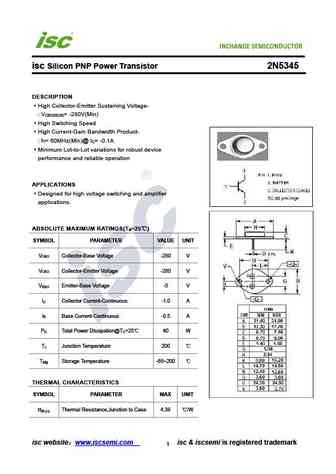
isc Silicon PNP Power Transistor 2N5345 DESCRIPTION High Collector-Emitter Sustaining Voltage- V = -280V(Min) CEO(SUS) High Switching Speed High Current-Gain Bandwidth Product- f = 60MHz(Min)@ I = -0.1A T C Minimum Lot-to-Lot variations for robust device performance and reliable operation APPLICATIONS Designed for high voltage switching and amplifier applications. AB... See More ⇒
0.35. Size:38K inchange semiconductor
2n5301.pdf 
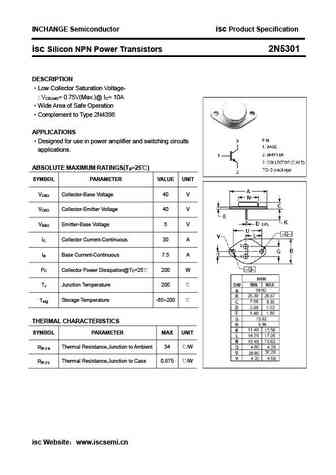
INCHANGE Semiconductor isc Product Specification isc Silicon NPN Power Transistors 2N5301 DESCRIPTION Low Collector Saturation Voltage- VCE(sat)= 0.75V(Max.)@ IC= 10A Wide Area of Safe Operation Complement to Type 2N4398 APPLICATIONS Designed for use in power amplifier and switching circuits applications. ABSOLUTE MAXIMUM RATINGS(Ta=25 ) SYMBOL PARAMETER VALU... See More ⇒
0.36. Size:196K inchange semiconductor
2n5302.pdf 
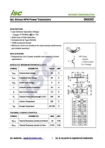
INCHANGE Semiconductor isc Silicon NPN Power Transistors 2N5302 DESCRIPTION Low Collector Saturation Voltage- V = 0.75V(Max.)@ I = 10A CE(sat) C Wide Area of Safe Operation Complement to Type 2N4399 100% avalanche tested Minimum Lot-to-Lot variations for robust device performance and reliable operation. APPLICATIONS Designed for use in power amplifier and switching cir... See More ⇒
0.37. Size:119K inchange semiconductor
2n5301 2n5302 2n5303.pdf 
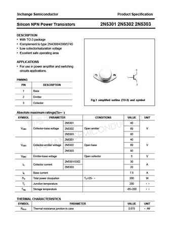
Inchange Semiconductor Product Specification Silicon NPN Power Transistors 2N5301 2N5302 2N5303 DESCRIPTION With TO-3 package Complement to type 2N4398/4399/5745 Low collector/saturation voltage Excellent safe operating area APPLICATIONS For use in power amplifier and switching circuits applications. PINNING PIN DESCRIPTION 1 Base 2 Emitter Fig.1 simplified o... See More ⇒
0.38. Size:51K inchange semiconductor
2n5344.pdf 
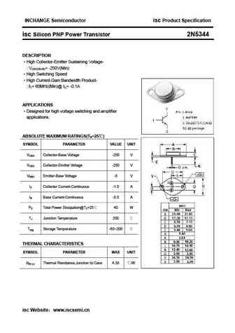
INCHANGE Semiconductor isc Product Specification isc Silicon PNP Power Transistor 2N5344 DESCRIPTION High Collector-Emitter Sustaining Voltage- VCEO(SUS)= -250V(Min) High Switching Speed High Current-Gain Bandwidth Product- fT= 60MHz(Min)@ IC= -0.1A APPLICATIONS Designed for high voltage switching and amplifier applications. ABSOLUTE MAXIMUM RATINGS(Ta=25 )... See More ⇒
Detailed specifications: 2N5291, 2N5292, 2N5293, 2N5294, 2N5295, 2N5296, 2N5297, 2N5298, S8050, 2N530, 2N5301, 2N5302, 2N5303, 2N5304, 2N5305, 2N5306, 2N5306A
Keywords - 2N53 pdf specs
2N53 cross reference
2N53 equivalent finder
2N53 pdf lookup
2N53 substitution
2N53 replacement
