2N5450 Specs and Replacement
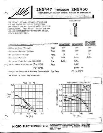
Type Designator: 2N5450
Material of Transistor: Si
Polarity: NPN
Absolute Maximum Ratings
Maximum Collector Power Dissipation (Pc): 0.36 W
Maximum Collector-Base Voltage |Vcb|: 50 V
Maximum Collector-Emitter Voltage |Vce|: 30 V
Maximum Emitter-Base Voltage |Veb|: 5 V
Maximum Collector Current |Ic max|: 0.8 A
Max. Operating Junction Temperature (Tj): 150 °C
Electrical Characteristics
Transition Frequency (ft): 100 MHz
Collector Capacitance (Cc): 12 pF
Forward Current Transfer Ratio (hFE), MIN: 50
Noise Figure, dB: -
2N5450 Substitution
- BJT ⓘ Cross-Reference Search
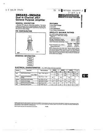
2N5450 datasheet
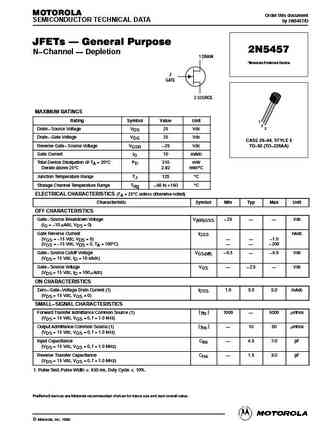
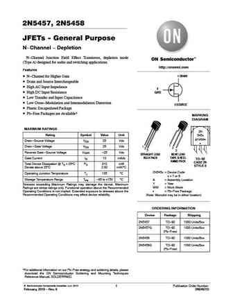
MOTOROLA Order this document SEMICONDUCTOR TECHNICAL DATA by 2N5457/D JFETs General Purpose 2N5457 N Channel Depletion 1 DRAIN *Motorola Preferred Device 3 GATE 2 SOURCE MAXIMUM RATINGS Rating Symbol Value Unit 1 2 3 Drain Source Voltage VDS 25 Vdc Drain Gate Voltage VDG 25 Vdc CASE 29 04, STYLE 5 Reverse Gate Source Voltage VGSR 25 Vdc TO 92 (TO 226AA)... See More ⇒
2n5457 2n5458 2n5459 mmbf5457 mmbf5458 mmbf5459.pdf ![]()
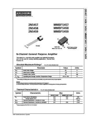
2N5457 MMBF5457 2N5458 MMBF5458 2N5459 MMBF5459 G S TO-92 G S SOT-23 NOTE Source & Drain D D are interchangeable Mark 6D / 61S / 6L N-Channel General Purpose Amplifier This device is a low level audio amplifier and switching transistors, and can be used for analog switching applications. Sourced from Process 55. Absolute Maximum Ratings* TA = 25 C unless otherwise noted S... See More ⇒
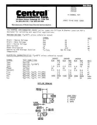
145 Adams Avenue, Hauppauge, NY 11788 USA Tel (631) 435-1110 Fax (631) 435-1824 ... See More ⇒
Detailed specifications: 2N5440, 2N544-12, 2N544-33, 2N5447, 2N5448, 2N5449, 2N544A, 2N545, C945, 2N5451, 2N5455, 2N5456, 2N546, 2N5466, 2N5467, 2N5468, 2N5469
Keywords - 2N5450 pdf specs
2N5450 cross reference
2N5450 equivalent finder
2N5450 pdf lookup
2N5450 substitution
2N5450 replacement
