2N6025 Datasheet. Specs and Replacement
Type Designator: 2N6025
Material of Transistor: Si
Polarity: PNP
Absolute Maximum Ratings
Maximum Collector Power Dissipation (Pc): 36 W
Maximum Collector-Base Voltage |Vcb|: 80 V
Maximum Collector-Emitter Voltage |Vce|: 60 V
Maximum Emitter-Base Voltage |Veb|: 5 V
Maximum Collector Current |Ic max|: 4 A
Max. Operating Junction Temperature (Tj): 150 °C
Electrical Characteristics
Transition Frequency (ft): 0.8 MHz
Forward Current Transfer Ratio (hFE), MIN: 30
Package: TO220
2N6025 Substitution
- BJT ⓘ Cross-Reference Search
2N6025 datasheet
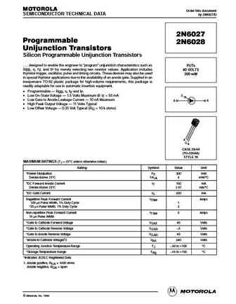
MOTOROLA Order this document SEMICONDUCTOR TECHNICAL DATA by 2N6027/D 2N6027 Programmable 2N6028 Unijunction Transistors Silicon Programmable Unijunction Transistors . . . designed to enable the engineer to program unijunction characteristics such as PUTs RBB, , IV, and IP by merely selecting two resistor values. Application includes 40 VOLTS thyristor-trigger, oscillator, ... See More ⇒
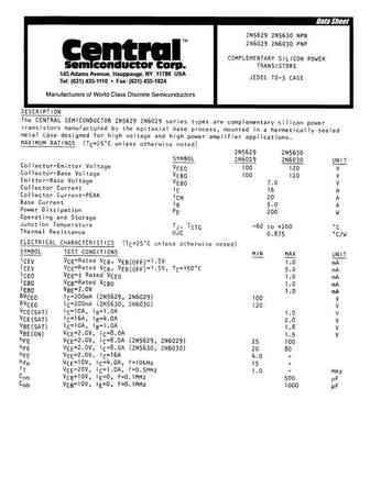
2n5629 2n5630 2n6029 2n6030.pdf ![]()
145 Adams Avenue, Hauppauge, NY 11788 USA Tel (631) 435-1110 Fax (631) 435-1824 ... See More ⇒
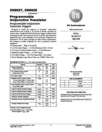
2N6027, 2N6028 Preferred Device Programmable Unijunction Transistor Programmable Unijunction Transistor Triggers Designed to enable the engineer to program unijunction http //onsemi.com characteristics such as RBB, , IV, and IP by merely selecting two resistor values. Application includes thyristor trigger, oscillator, pulse PUTs and timing circuits. These devices may als... See More ⇒
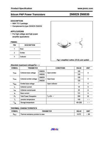
Product Specification www.jmnic.com Silicon PNP Power Transistors 2N6029 2N6030 DESCRIPTION With TO-3 package Complement to type 2N5629 2N5630 APPLICATIONS For high voltage and high power amplifier applications PINNING PIN DESCRIPTION 1 Base 2 Emitter 3 Collector Fig.1 simplified outline (TO-3) and symbol Absolute maximum ratings(Ta= ) SYMBOL PARAMETER CONDITI... See More ⇒
Detailed specifications: 2N6014, 2N6015, 2N6016, 2N6017, 2N602, 2N6021, 2N6022, 2N6024, 13007, 2N6026, 2N6029, 2N602A, 2N603, 2N6030, 2N6031, 2N6032, 2N6033
Keywords - 2N6025 pdf specs
2N6025 cross reference
2N6025 equivalent finder
2N6025 pdf lookup
2N6025 substitution
2N6025 replacement


