2N6076 Specs and Replacement
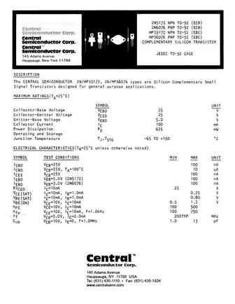
Type Designator: 2N6076
Material of Transistor: Si
Polarity: NPN
Absolute Maximum Ratings
Maximum Collector Power Dissipation (Pc): 0.36 W
Maximum Collector-Base Voltage |Vcb|: 25 V
Maximum Collector-Emitter Voltage |Vce|: 25 V
Maximum Emitter-Base Voltage |Veb|: 5 V
Maximum Collector Current |Ic max|: 0.1 A
Max. Operating Junction Temperature (Tj): 125 °C
Electrical Characteristics
Transition Frequency (ft): 100 MHz
Collector Capacitance (Cc): 13 pF
Forward Current Transfer Ratio (hFE), MIN: 100
Noise Figure, dB: -
Package: TO92
- BJT ⓘ Cross-Reference Search
2N6076 datasheet
..1. Size:29K fairchild semi
2n6076.pdf 

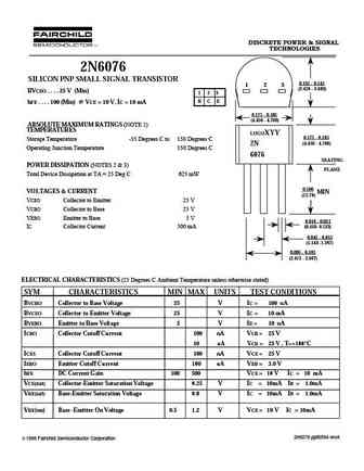
DISCRETE POWER & SIGNAL TECHNOLOGIES 2N6076 SILICON PNP SMALL SIGNAL TRANSISTOR 0.135 - 0.145 1 2 3 (3.429 - 3.683) BVCEO . . . . 25 V (Min) 1 2 3 B C E hFE . . . . 100 (Min) @ VCE = 10 V, IC = 10 mA 0.175 - 0.185 (4.450 - 4.700) ABSOLUTE MAXIMUM RATINGS (NOTE 1) TEMPERATURES LOGOXYY 0.175 - 0.185 Storage Temperature -55 Degrees C to 150 Degrees C (4.450 - 4.700) 2N Op... See More ⇒
9.1. Size:118K motorola
2n6071 2n6073 2n6075.pdf 

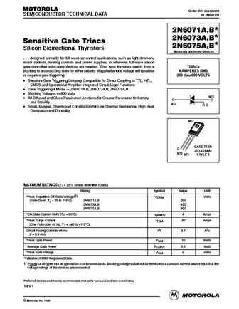
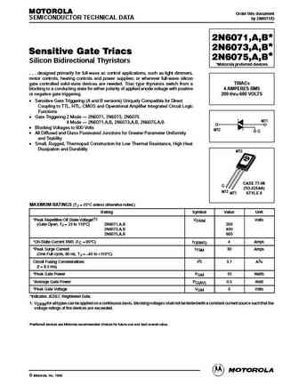
MOTOROLA Order this document SEMICONDUCTOR TECHNICAL DATA by 2N6071/D * 2N6071A,B * 2N6073A,B Sensitive Gate Triacs 2N6075A,B* Silicon Bidirectional Thyristors *Motorola preferred devices . . . designed primarily for full-wave ac control applications, such as light dimmers, motor controls, heating controls and power supplies; or wherever full-wave silicon gate controlled solid-sta... See More ⇒
9.2. Size:157K motorola
2n6071 2n6073 2n6075 .pdf 

MOTOROLA Order this document SEMICONDUCTOR TECHNICAL DATA by 2N6071/D * 2N6071,A,B * 2N6073,A,B Sensitive Gate Triacs 2N6075,A,B* Silicon Bidirectional Thyristors *Motorola preferred devices . . . designed primarily for full-wave ac control applications, such as light dimmers, motor controls, heating controls and power supplies; or wherever full-wave silicon TRIACs gate controlle... See More ⇒
9.3. Size:10K semelab
2n6077.pdf 

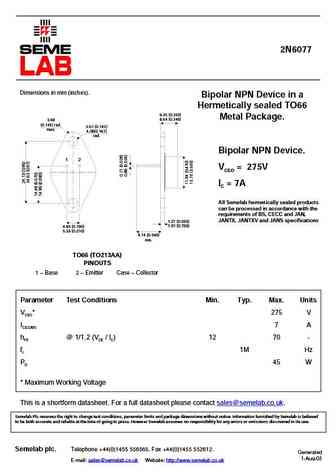
2N6077 Dimensions in mm (inches). Bipolar NPN Device in a Hermetically sealed TO66 6.35 (0.250) Metal Package. 8.64 (0.340) 3.68 (0.145) rad. 3.61 (0.142) max. 4.08(0.161) rad. Bipolar NPN Device. 1 2 VCEO = 275V IC = 7A All Semelab hermetically sealed products can be processed in accordance with the requirements of BS, CECC and JAN, JANTX, JANTXV and JANS speci... See More ⇒
9.4. Size:10K semelab
2n6079.pdf 

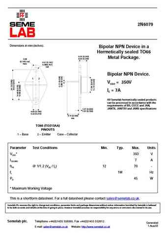
2N6079 Dimensions in mm (inches). Bipolar NPN Device in a Hermetically sealed TO66 6.35 (0.250) Metal Package. 8.64 (0.340) 3.68 (0.145) rad. 3.61 (0.142) max. 4.08(0.161) rad. Bipolar NPN Device. 1 2 VCEO = 350V IC = 7A All Semelab hermetically sealed products can be processed in accordance with the requirements of BS, CECC and JAN, JANTX, JANTXV and JANS speci... See More ⇒
9.5. Size:17K semelab
2n6078.pdf 

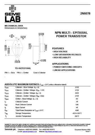
2N6078 MECHANICAL DATA Dimensions in mm(inches) NPN MULTI - EPITAXIAL 6.35 (0.250) 8.64 (0.340) 3.68 (0.145) rad. 3.61 (0.142) POWER TRANSISTOR max. 4.08(0.161) rad. 1 2 FEATURES HIGH VOLTAGE LOW SATURATION VOLTAGES HIGH RELIABILITY 1.27 (0.050) 4.83 (0.190) 1.91 (0.750) 5.33 (0.210) 9.14 (0.360) APPLICATIONS min. POWER SWITCHING CIRCUITS TO 66(TO213AA... See More ⇒
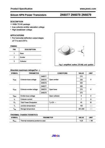
9.6. Size:116K jmnic
2n6077 2n6078 2n6079.pdf 

Product Specification www.jmnic.com Silicon NPN Power Transistors 2N6077 2N6078 2N6079 DESCRIPTION With TO-66 package Low collector-emitter saturation voltage High breakdown voltage APPLICATIONS For horizontal deflection output stages of TV s and CRT s PINNING PIN DESCRIPTION 1 Base 2 Emitter 3 Collector Fig.1 simplified outline (TO-66) and symbol Abso... See More ⇒
9.7. Size:186K inchange semiconductor
2n6078.pdf 
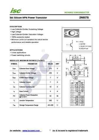
isc Silicon NPN Power Transistor 2N6078 DESCRIPTION Low Collector-Emitter Sustaining Voltage High voltage Low Collector-Emitter Saturation Voltage- 100% avalanche tested Minimum Lot-to-Lot variations for robust device performance and reliable operation APPLICATIONS Linear applications Power switching circuits ABSOLUTE MAXIMUM RATINGS (T =25 ) a SYMBOL PARAMETER VALU... See More ⇒
9.8. Size:127K inchange semiconductor
2n6077 2n6078 2n6079.pdf 
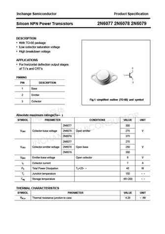
Inchange Semiconductor Product Specification Silicon NPN Power Transistors 2N6077 2N6078 2N6079 DESCRIPTION With TO-66 package Low collector saturation voltage High breakdown voltage APPLICATIONS For horizontal deflection output stages of TV s and CRT s PINNING PIN DESCRIPTION 1 Base 2 Emitter Fig.1 simplified outline (TO-66) and symbol 3 Collector Absolut... See More ⇒
Detailed specifications: 2N6061, 2N6062, 2N6063, 2N6064, 2N6065, 2N6066, 2N6067, 2N607, 2222A, 2N6077, 2N6078, 2N6079, 2N608, 2N6080, 2N6081, 2N6082, 2N6083
Keywords - 2N6076 pdf specs
2N6076 cross reference
2N6076 equivalent finder
2N6076 pdf lookup
2N6076 substitution
2N6076 replacement
![]()
