2N6219 Specs and Replacement
Type Designator: 2N6219
Material of Transistor: Si
Polarity: NPN
Absolute Maximum Ratings
Maximum Collector Power Dissipation (Pc): 0.5 W
Maximum Collector-Base Voltage |Vcb|: 250 V
Maximum Collector-Emitter Voltage |Vce|: 250 V
Maximum Emitter-Base Voltage |Veb|: 5 V
Maximum Collector Current |Ic max|: 0.05 A
Max. Operating Junction Temperature (Tj): 150 °C
Electrical Characteristics
Transition Frequency (ft): 50 MHz
Collector Capacitance (Cc): 5 pF
Forward Current Transfer Ratio (hFE), MIN: 20
Package: TO92
2N6219 Substitution
- BJT ⓘ Cross-Reference Search
2N6219 datasheet
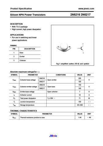
Product Specification www.jmnic.com Silicon NPN Power Transistors 2N6216 2N6217 DESCRIPTION With TO-3 package High current ,high power dissipation APPLICATIONS For use in switching and linear power applications PINNING PIN DESCRIPTION 1 Base 2 Emitter 3 Collector Fig.1 simplified outline (TO-3) and symbol Absolute maximum ratings(Ta= ) SYMBOL PARAMETER CONDITI... See More ⇒
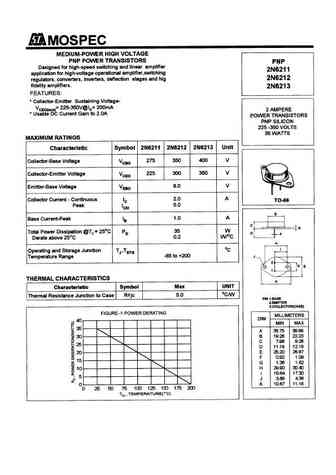
INCHANGE Semiconductor isc Silicon PNP Power Transistor 2N6211 DESCRIPTION High Collector-Emitter Sustaining Voltage- V = -225V(Min) CEO(SUS) Good Linearity of h FE Minimum Lot-to-Lot variations for robust device performance and reliable operation APPLICATIONS Designed for high-speed switching and linear amplifier application for high-voltage operational amplifier, switchi... See More ⇒
Inchange Semiconductor Product Specification Silicon NPN Power Transistors 2N6216 2N6217 DESCRIPTION With TO-3 package High current ,high power dissipation APPLICATIONS For use in switching and linear power applications PINNING PIN DESCRIPTION 1 Base 2 Emitter Fig.1 simplified outline (TO-3) and symbol 3 Collector Absolute maximum ratings(Ta= ) SYMBOL PARAMETE... See More ⇒
Detailed specifications: 2N6211, 2N6212, 2N6213, 2N6214, 2N6215, 2N6216, 2N6217, 2N6218, TIP32C, 2N622, 2N6220, 2N6221, 2N6222, 2N6223, 2N6224, 2N6225, 2N6226
Keywords - 2N6219 pdf specs
2N6219 cross reference
2N6219 equivalent finder
2N6219 pdf lookup
2N6219 substitution
2N6219 replacement
History: BD287 | BD292 | 2N6220 | 2N622 | 40325 | ZTX510L | ZTX504L
🌐 : EN ES РУ
LIST
Last Update
BJT: GA1A4M | SBT42 | 2SA200-Y | 2SA200-O | 2SD882-Q | 2SD882-P
Popular searches
2n5133 datasheet | 2sa726 transistor | 7506 mosfet | irlr8726 datasheet | ru7088r mosfet | mp40 transistor | fgpf4636 datasheet | 2sc1945


